Hostname: page-component-78c5997874-ndw9j Total loading time: 0 Render date: 2024-11-17T16:30:43.686Z Has data issue: false hasContentIssue false

Effect of Al3+/Si4+ codoping on the structural, optoelectronic and UV sensing properties of ZnO

Published online by Cambridge University Press:  15 May 2020

Saniya Ayaz
Affiliation:
Metallurgical Engineering and Material Science, Indian Institute of Technology, Indore 453552, India
Neha Sharma
Affiliation:
Department of Physics, Deenbandhu Chhotu Ram University of Science and Technology, Sonepat, Haryana 131039, India
Aditya Dash
Affiliation:
Department of Physics and Astronomy, National Institute of Technology Rourkela, Odisha, 769008, India
Somaditya Sen*
Affiliation:
Discipline of Physics, Indian Institute of Technology Indore, Indore 453552, India Electronic Engineering, Ming Chi University of Technology, New Taipei City 24301, Taiwan.
*
a)Address all correspondence to this author. e-mail: sens@iiti.ac.in
Get access

Abstract

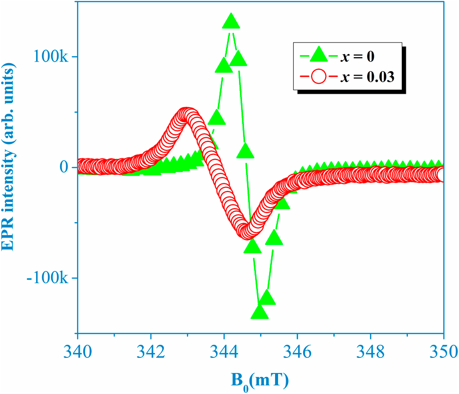
The structural, vibrational, and optoelectronic properties of sol–gel synthesized Zn1−x(Al0.5Si0.5)xO nanoparticles were investigated. The X-ray diffraction studies of the samples confirmed the hexagonal wurtzite phase with the space group P63mc. No significant changes were observed in the lattice parameters. The increase in the intensity of $E_{{\rm{high}}}^2$ Raman mode observed at 438 cm−1 indicates a decrease in the crystallite size. The reduction in the deep-level emission band with the introduction of Al/Si indicates a decrease in intrinsic defects for the codoped sample. A unique electron paramagnetic resonance signal at g= 1.96 follows the same trend as the green luminescence, and its evolution was shown to probe the oxygen vacancy concentrations. IV characteristics curve confirm the increase in the conductivity for the codoped samples. To evaluate the role of surface defects, ultraviolet photoresponse behavior as a function of time was also studied, and an increase in the photocurrent was observed. The slow decay and rise in the photocurrent are because of multiple trapping by interstitial defects. A relatively faster response time was observed with the substitution of Al/Si. It has been observed that prepared nanomaterials are suitable for optoelectronic devices.

Type
Article
Copyright
Copyright © Materials Research Society 2020

Access options

Get access to the full version of this content by using one of the access options below. (Log in options will check for institutional or personal access. Content may require purchase if you do not have access.)

References

McDermott, E.J., Kurmaev, E.Z., Boyko, T.D., Finkelstein, L.D., Green, R.J., Maeda, K., Domen, K., and Moewes, A.: Structural and band gap investigation of GaN:ZnO heterojunction solid solution photocatalyst probed by soft X-ray spectroscopy. J. Phys. Chem. C 116, 7694 (2012).CrossRefGoogle Scholar
Hsu, C-L., Wang, Y-C., Chang, S-P., and Chang, S-J.: Ultraviolet/visible photodetectors based on p–n NiO/ZnO nanowires decorated with Pd nanoparticles. ACS Appl. Nano Mater. 2, 6343 (2019).CrossRefGoogle Scholar
Cao, S., Zheng, J., Zhao, J., Yang, Z., Li, C., Guan, X., Yang, W., Shang, M., and Wu, T.: Enhancing the performance of quantum dot light-emitting diodes using room-temperature-processed Ga-doped ZnO nanoparticles as the electron transport layer. ACS Appl. Mater. Interfaces 9, 15605 (2017).CrossRefGoogle ScholarPubMed
Dahiya, A.S., Opoku, C., Poulin-Vittrant, G., Camara, N., Daumont, C., Barbagiovanni, E.G., Franzò, G., Mirabella, S., and Alquier, D.: Flexible organic/inorganic hybrid field-effect transistors with high performance and operational stability. ACS Appl. Mater. Interfaces 9, 573 (2017).CrossRefGoogle ScholarPubMed
Zhu, L., Zhang, Y., Lin, P., Wang, Y., Yang, L., Chen, L., Wang, L., Chen, B., and Wang, Z.L.: Piezotronic effect on rashba spin–orbit coupling in a ZnO/P3HT nanowire array structure. ACS Nano 12, 1811 (2018).CrossRefGoogle Scholar
Dai, J., Suo, Z., Li, Z., and Gao, S.: Effect of Cu/Al doping on electronic structure and optical properties of ZnO. Results Phys. 15, 102649 (2019).CrossRefGoogle Scholar
Hullavarad, S., Hullavarad, N., Look, D., and Claflin, B.: Persistent photoconductivity studies in nanostructured ZnO UV sensors. Nanoscale Res. Lett. 4, 1421 (2009).CrossRefGoogle ScholarPubMed
Gimenez, A.J., Yanez-Limon, J., and Seminario, J.M.: ZnO–paper based photoconductive UV sensor. J. Phys. Chem. C 115, 282 (2010).CrossRefGoogle Scholar
Liu, K., Sakurai, M., and Aono, M.: ZnO-based ultraviolet photodetectors. Sensors 10, 8604 (2010).CrossRefGoogle ScholarPubMed
Arif, M., Shkir, M., AlFaify, S., Ganesh, V., Sanger, A., Algarni, H., Vilarinho, P.M., and Singh, A.: A structural, morphological, linear, and nonlinear optical spectroscopic studies of nanostructured Al-doped ZnO thin films: An effect of Al concentrations. J. Mater. Res. 34, 1309 (2019).CrossRefGoogle Scholar
Ponja, S.D., Sathasivam, S., Parkin, I.P., and Carmalt, C.J.: Highly conductive and transparent gallium doped zinc oxide thin films via chemical vapor deposition. Sci. Rep. 10, 638 (2020).CrossRefGoogle ScholarPubMed
Caglar, M., Caglar, Y., and Ilican, S.: Electrical and optical properties of undoped and In-doped ZnO thin films. Phys. Status Solidi C 4, 1337 (2007).CrossRefGoogle Scholar
El Hallani, G., Nasih, S., Fazouan, N., Liba, A., Khuili, M., Sajieddine, M., Mabrouki, M., Laanab, L., and Atmani, E.: Comparative study for highly Al and Mg doped ZnO thin films elaborated by sol gel method for photovoltaic application. J. Appl. Phys. 121, 135103 (2017).CrossRefGoogle Scholar
Nomoto, J., Makino, H., Nakajima, T., Tsuchiya, T., and Yamamoto, T.: Improvement of the properties of direct-current magnetron-sputtered Al-doped ZnO polycrystalline films containing retained Ar atoms using 10-nm-thick buffer layers. ACS omega 4, 1452614536 (2019).CrossRefGoogle ScholarPubMed
Cao, Y-T., Cai, Y., Yao, C-B., Bao, S-B., and Han, Y.: The photoluminescence, field emission and femtosecond nonlinear absorption properties of Al-doped ZnO nanowires, nanobelts, and nanoplane-cone morphologies. RSC Adv. 9, 34547 (2019).CrossRefGoogle Scholar
Liu, Y., Zhang, H., An, X., Gao, C., Zhang, Z., Zhou, J., Zhou, M., and Xie, E.: Effect of Al doping on the visible photoluminescence of ZnO nanofibers. J. Alloys Compd. 506, 772 (2010).CrossRefGoogle Scholar
Srivastava, T., Kumar, S., Shirage, P., and Sen, S.: Reduction of O2– related defect states related to increased bandgap in Si4+ substituted ZnO. Scr. Mater. 124, 11 (2016).CrossRefGoogle Scholar
Warren, B.E.: X-ray Diffraction. Dover publications, INC., New York (1990).Google Scholar
Russo, V., Ghidelli, M., Gondoni, P., Casari, C.S., and Li Bassi, A.: Multi-wavelength Raman scattering of nanostructured Al-doped zinc oxide. J. Appl. Phys. 115, 073508 (2014).CrossRefGoogle Scholar
Damen, T.C., Porto, S., and Tell, B.: Raman effect in zinc oxide. Phys. Rev. 142, 570 (1966).CrossRefGoogle Scholar
Luo, J., Zhu, X., Chen, G., Zeng, F., and Pan, F.: The electrical, optical, and magnetic properties of Si-doped ZnO films. Appl. Surf. Sci. 258, 2177 (2012).CrossRefGoogle Scholar
Biroju, R.K. and Giri, P.: Strong visible and near infrared photoluminescence from ZnO nanorods/nanowires grown on single layer graphene studied using sub-band gap excitation. J. Appl. Phys. 122, 044302 (2017).CrossRefGoogle Scholar
Dhara, S. and Giri, P.: Enhanced UV photosensitivity from rapid thermal annealed vertically aligned ZnO nanowires. Nanoscale Res. Lett. 6, 504 (2011).CrossRefGoogle ScholarPubMed
Xiong, G., Pal, U., and Serrano, J.G.: Correlations among size, defects, and photoluminescence in ZnO nanoparticles. J. Appl. Phys. 101, 024317 (2007).CrossRefGoogle Scholar
Lv, J. and Li, X.: Defect evolution in ZnO and its effect on radiation tolerance. Phys. Chem. Chem. Phys. 20, 11882 (2018).CrossRefGoogle ScholarPubMed
Thomas, D., Sadasivuni, K.K., Waseem, S., Kumar, B., and Cabibihan, J-J.: Synthesis, green emission and photosensitivity of Al-doped ZnO film. Microsyst. Technol. 24, 3069 (2018).CrossRefGoogle Scholar
Kaftelen, H., Ocakoglu, K., Thomann, R., Tu, S., Weber, S., and Erdem, E.: EPR and photoluminescence spectroscopy studies on the defect structure of ZnO nanocrystals. Phys. Rev. B 86, 014113 (2012).CrossRefGoogle Scholar
Lv, J., Li, C., and BelBruno, J.: Characteristics of point defects on the optical properties of ZnO: Revealed by Al–H co-doping and post-annealing. RSC Adv. 3, 8652 (2013).CrossRefGoogle Scholar
Drouilly, C., Krafft, J-M., Averseng, F., Casale, S., Bazer-Bachi, D., Chizallet, C., Lecocq, V., Vezin, H., Lauron-Pernot, H., and Costentin, G.: ZnO oxygen vacancies formation and filling followed by in situ photoluminescence and in situ EPR. J. Phys. Chem. C 116, 21297 (2012).CrossRefGoogle Scholar
Gurwitz, R., Cohen, R., and Shalish, I.: Interaction of light with the ZnO surface: Photon induced oxygen “breathing,” oxygen vacancies, persistent photoconductivity, and persistent photovoltage. J. Appl. Phys. 115, 033701 (2014).CrossRefGoogle Scholar
Bera, A. and Basak, D.: Role of defects in the anomalous photoconductivity in ZnO nanowires. Appl. Phys. Lett. 94, 163119 (2009).CrossRefGoogle Scholar
Barbagiovanni, E., Strano, V., Franzò, G., Crupi, I., and Mirabella, S.: Photoluminescence transient study of surface defects in ZnO nanorods grown by chemical bath deposition. Appl. Phys. Lett. 106, 093108 (2015).CrossRefGoogle Scholar
Kayaci, F., Vempati, S., Donmez, I., Biyikli, N., and Uyar, T.: Role of zinc interstitials and oxygen vacancies of ZnO in photocatalysis: A bottom-up approach to control defect density. Nanoscale 6, 10224 (2014).CrossRefGoogle ScholarPubMed