We use cookies to distinguish you from other users and to provide you with a better experience on our websites. Close this message to accept cookies or find out how to manage your cookie settings.
To save content items to your account,
please confirm that you agree to abide by our usage policies.
If this is the first time you use this feature, you will be asked to authorise Cambridge Core to connect with your account.
Find out more about saving content to .
To save content items to your Kindle, first ensure coreplatform@cambridge.org
is added to your Approved Personal Document E-mail List under your Personal Document Settings
on the Manage Your Content and Devices page of your Amazon account. Then enter the ‘name’ part
of your Kindle email address below.
Find out more about saving to your Kindle.
Note you can select to save to either the @free.kindle.com or @kindle.com variations.
‘@free.kindle.com’ emails are free but can only be saved to your device when it is connected to wi-fi.
‘@kindle.com’ emails can be delivered even when you are not connected to wi-fi, but note that service fees apply.
This article argues for a renewal of the discipline of New Testament studies through a focus on the question of truth. To make the argument, the article first engages a recent essay that is highly critical of mainstream NT scholarship and subsequently works with the thought of Søren Kierkegaard, Stanley Cavell, Cora Diamond and Hans-Georg Gadamer to pursue the interpreter's implications in the NT's assertions of truth. The article also briefly exegetes five passages from the NT to illustrate the way the NT makes claims that require judgements about truth. Along the way, the article also engages contemporary NT scholars who argue vociferously against ‘theological’ readings of the NT and others who argue for their inherent necessity.
Stimulated Raman-scattering-based lasers provide an effective way to achieve wavelength conversion. However, thermally induced beam degradation is a notorious obstacle to power scaling and it also limits the applicable range where high output beam quality is needed. Considerable research efforts have been devoted to developing Raman materials, with diamond being a promising candidate to acquire wavelength-versatile, high-power, and high-quality output beam owing to its excellent thermal properties, high Raman gain coefficient, and wide transmission range. The diamond Raman resonator is usually designed as an external-cavity pumped structure, which can easily eliminate the negative thermal effects of intracavity laser crystals. Diamond Raman converters also provide an approach to improve the beam quality owing to the Raman cleanup effect. This review outlines the research status of diamond Raman lasers, including beam quality optimization, Raman conversion, thermal effects, and prospects for future development directions.
This article reports findings when using a molybdenum–tungsten (MoW) interlayer for diamond thin film deposition on steel substrates. The main focus was on the postdeposition stress within the diamond films and its impact on the coating's tribological properties. The effect of MoW interlayer thickness and the effect of chemical vapor deposition (CVD) process temperature have been investigated. Nanocrystalline diamond films were deposited on steel substrates with MoW interlayers (thickness of 1.1, 4.5, and 8.3 μm) at two different deposition temperatures (650 and 875 °C). It was found that when depositing good quality diamond films on steel substrates, increasing interlayer thickness and decreasing CVD process temperature have to be jointly considered to obtain the optimal result. The diamond-coated steel substrates with the 8.3 μm interlayer deposited at the lower CVD processing temperature exhibited the least residual stress combined with excellent mechanical properties.
To study the interface characteristics between substrates and homoepitaxially grown single crystalline diamond layers, the high-pressure/high-temperature Ib diamond seeds with homoepitaxial diamond layers were annealed by low-pressure/high-temperature treatment in a hydrogen environment. The stress evolution and related impurity transformation near the interface were characterized by Raman spectroscopy, photoluminescence, and micro-infrared spectroscopy before and after annealing. It is found that the stress is the smallest in a 100 μm wide zone near the interface, accompanying with the similar change in substitutional nitrogen (Ns) concentration. After annealing at 1050 °C, 1250 °C, and 1450 °C, the local compressive stress is released gradually with temperature change. It is decreased by 1.03 GPa in maximum after annealing at 1450 °C. The concentration of nitrogen–vacancy (NV) complexes in the chemical vapor deposition (CVD) layer is dramatically reduced at 1450 °C. The value of 
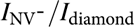
${{I_{{\rm{NV}}^ \hbox- } } \mathord{\left/ {\vphantom {{I_{{\rm{NV}}^ - } } {I_{{\rm{diamond}}} }}} \right. \kern-\nulldelimiterspace} {I_{{\rm{diamond}}} }}$ decreases much more than ${{I_{{\rm{NV}}^0 } } \mathord{\left/ {\vphantom {{I_{{\rm{NV}}^0 } } {I_{{\rm{diamond}}} }}} \right. \kern-\nulldelimiterspace} {I_{{\rm{diamond}}} }}$ in the CVD layer, which is due to the lower stability of NV− compared with NV0 at high temperature.
The development of GaN-on-diamond devices offers bright prospects for the creation of high-power density electronics. This article presents a process of fabricating GaN-on-diamond structure by depositing diamond films on dual sides, including heat dissipation diamond film and sacrificial carrier diamond film. Prior to heat dissipation diamond film layer preparation, aluminum nitride (AlN) is chosen as a dielectric layer and pretreated by nanodiamond (ND) particles, to enhance the nucleation density. Zeta potential measurements and X-ray photoelectron spectroscopy are used to analyze the AlN surface after each treatment. The results show that oxygen-terminated ND particles tend to adhere to an AlN surface because the oxygen-terminated NDs have –COOH and –OH groups, and hold a negative potential. On the contrary, fluorine-terminated AlN prefers to attract the hydrogen-terminated ND seeds, which resulted in higher diamond nucleation density. Based on this preliminary study, a dense high-quality GaN-on-diamond wafer is successfully produced by using AlN as the dielectric layer and a diamond film as the sacrificial carrier.
We are proposing a novel fabrication method for single crystal diamond scanning probes for atomic force microscopy (AFM), exploiting Faraday cage angled etching (FCAE). Common, oxygen-based, inductively coupled plasma (ICP) dry etching processes for diamond are limited with respect to the achievable geometries. The fabrication of freestanding micro- and nanostructures is therefore challenging. This is a major disadvantage for several application fields e.g., for realizing scanning magnetometry probes based on nitrogen vacancy (NV) centres and capable of measuring magnetic fields at the nanoscale. Combining a planar design with FCAE and state-of-the-art electron beam lithography (EBL) yields a reduction of process complexity and cost compared to the established fabrication technology of micro-opto-mechanical diamond devices. Here, we report on the direct comparison of both approaches and present first proof-of-concept planar-FCAE-prototypes for scanning probe applications.
This chapter reviews the distribution of carbon-bearing phases in the crust, mantle, and the core. It presents conditions of stability of various carbon-bearing phases – such as carbonate minerals, carbon-bearing fluids, graphite, diamond, and carbides – and how these stabilities put limits on the carbon budget of the mantle. The chapter also discusses expectations about how stability may have varied throughout geologic time, given the thermal and redox evolution of the Earth. Finally, this chapter also presents recent discoveries about carbon mineral evolution.
We have investigated a diamond crystal that consists of several misorientated subgrains. The main feature of the crystal is the dark areas in the cathodoluminescent core that has ‘estuary-like’ boundaries extending along the subgrain interfaces. The core has >3100 ppm of nitrogen, and the share of the B form is >95%; the absorbance of the centre N3VH at 3107 cm–1 reaches 75 cm–1. The N3 centre absorbance, as well as N3 luminescence, is absent in the core. In the outer part of the crystal, bright blue luminescence of the N3 centre is apparent, and the N3 absorbance reaches 5.3 cm–1. These observations could be explained by the conversion of N3 centres to N3VH after attaching a hydrogen atom. After the full conversion of the N3 centres, the diamond becomes darker under CL. We hypothesise the dark core has a specific shape due to the post-growth diffusion of the hydrogen.
This work demonstrates the in situ growth of carbon nanowalls (CNWs) on diamond semiconductors by microwave plasma-assisted chemical vapor deposition. The resulting CNW/diamond junctions behave as photomemristors having both photocontrollable multiple resistance states and nonvolatile memory functions. The resistance state (high or low resistance) can be selected by irradiation with blue or violet light in conjunction with the application of a bias voltage, giving a large resistance switching ratio of ∼106. The photoinduced resistance switching behaviors are rarely observed and has only been observed in a few materials and/or heterostructures. These junctions also exhibit a photoresponsivity of ∼12 A/W, which is much larger than that obtained from photodiodes composed of other materials. These results suggest that CNW/diamond (i.e., carbon sp2/sp3) junctions could have applications in novel photocontrollable devices, which have photosensing, memory, and switching functions.
We derive a forcing axiom from the conjunction of square and diamond, and present a few applications, primary among them being the existence of super-Souslin trees. It follows that for every uncountable cardinal $\unicode[STIX]{x1D706}$, if $\unicode[STIX]{x1D706}^{++}$ is not a Mahlo cardinal in Gödel’s constructible universe, then $2^{\unicode[STIX]{x1D706}}=\unicode[STIX]{x1D706}^{+}$ entails the existence of a $\unicode[STIX]{x1D706}^{+}$-complete $\unicode[STIX]{x1D706}^{++}$-Souslin tree.
We investigate which filters on ω can contain towers, that is, a modulo finite descending sequence without any pseudointersection (in ${[\omega ]^\omega }$). We prove the following results:
(1) Many classical examples of nice tall filters contain no towers (in ZFC).
(2) It is consistent that tall analytic P-filters contain towers of arbitrary regular height (simultaneously for many regular cardinals as well).
(3) It is consistent that all towers generate nonmeager filters (this answers a question of P. Borodulin-Nadzieja and D. Chodounský), in particular (consistently) Borel filters do not contain towers.
(4) The statement “Every ultrafilter contains towers.” is independent of ZFC (this improves an older result of K. Kunen, J. van Mill, and C. F. Mills).
Furthermore, we study many possible logical (non)implications between the existence of towers in filters, inequalities between cardinal invariants of filters (${\rm{ad}}{{\rm{d}}^{\rm{*}}}\left( {\cal F} \right)$, ${\rm{co}}{{\rm{f}}^{\rm{*}}}\left( {\cal F} \right)$, ${\rm{no}}{{\rm{n}}^{\rm{*}}}\left( {\cal F} \right)$, and ${\rm{co}}{{\rm{v}}^{\rm{*}}}\left( {\cal F} \right)$), and the existence of Luzin type families (of size $\ge {\omega _2}$), that is, if ${\cal F}$ is a filter then ${\cal X} \subseteq {[\omega ]^\omega }$ is an ${\cal F}$-Luzin family if 
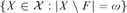
$\left\{ {X \in {\cal X}:|X \setminus F| = \omega } \right\}$ is countable for every $F \in {\cal F}$.
The unique electronic structure of diamond and its excellent thermal properties allow a broad range of possible applications; from electron sources to RF electronics. However, knowledge of the surface energy levels is essential to produce efficient, high-quality devices. We investigate the valence band position and resulting negative electron affinity for hydrogen terminated diamond under ambient, low vacuum and ultra-high vacuum (UHV) conditions. There was a -0.5 eV change in valence band position causing a negative electron affinity shift from -1.1 eV under UHV to -0.6 eV in ambient pressure. We compare the photoemission current under each environment to predict the ability of the sample to be used as an electron source. The maximum emission was observed when the sample displayed the largest negative affinity. A scanning photoemission measurement is demonstrated to highlight the superior photoemission yield from the hydrogen terminated diamond surface compared to the stainless steel contact. A scanning Kelvin probe measurement is shown to illustrate a method of analyzing the contact potential difference across the diamond surface. Within high-power RF electronics, devices are likely to be operating at increased temperatures so knowledge of the impact of temperature on the energy levels is important. We study the valence band and Fermi level positions for hydrogen terminated diamond from room temperature (300K) to 425K under low and UHV conditions. The Fermi level moved below the valence band edge at increased temperature, illustrating the effect of the 2D hole gas at the surface. We also analyzed the photoemission characteristics and found an increase in yield with increasing temperature. The measurement techniques used to evaluate the energy levels of diamond: photoemission spectroscopy and Kelvin probe measurements, in ambient and vacuum, allow analysis to be completed in minutes. This offers an initial analysis alternative to elucidate more information and predict performance prior to the more time-consuming full device manufacture and characterization.
With a high affinity to carbon comparable to titanium and an electrically conductive carbide, zirconium has potential to form ohmic contact on boron doped diamond. In this work, formation of ohmic contacts on boron doped diamond using zirconium is studied in comparison to titanium. Boron doped diamond epitaxial layers have been grown by microwave plasma enhanced chemical vapour deposition with various B/C ratio. Circular Transmission Line Model structures were fabricated using standard micro-fabrication technologies. Specific contact resistance of fabricated contacts was determined for different boron concentrations and for various annealing temperatures. Ohmic contacts using zirconium are formed after annealing at 400 °C. Specific contact resistance steadily decreases with high temperature annealing down to a value of ca. 1 mΩ.cm2 after annealing at 700 °C for highly boron doped diamond. In comparison, titanium contact fabricated on highly doped diamond appears not stable under high temperature annealing.
Using dissipative particle dynamics approach, we model phase separation in a ternary system encompassing cross-linked polyacrylamide (PAM) gel, oil and water. PAM gels are widely used in many applications, from food and cosmetic applications to enhanced oil recovery approaches. We show that the PAM nanogel adsorbs at the oil-water interface and spreads out over this interface for the case of a loosely cross-linked polymer network. Tailoring PAM behavior at the oil-water interfaces by controlling gel’s properties could allow one to alter the properties of oil-water emulsions.
Catalytic behavior of colloidal dispersions of different nanocarbon additives in mineral and synthetic oil has been studied. Oxidation performance of mineral oil and synthetic oil containing detonation nanodiamonds (NDs/DNDs), detonation soot and commercial analogs have been compared with fullerenes and a conventional chemical antioxidant. Degradation characteristics of the oils were determined by total acid number (TAN) and Fourier transform infrared spectroscopy (FTIR). Both fullerenes and DNDs showed antioxidant properties in mineral oil, with DND performance depending on the method of deagglomeration. Antioxidant performance of DNDs and fullerenes in polyalphaolefin (PAO) oil is apparently less effective than in mineral oil.
This article argues that migration and investment from India moved in tandem to chart the evolution of transnational Indian business in the twentieth century, first toward Southeast Asia and Africa and later toward the United States, Europe, and West Asia. With a focus on the banking and diamond sectors, the overseas investment project of the Aditya Birla Group, and the transnational linkages of India's one hundred richest business leaders, the article locates important events, policies, and actors before economic liberalization in 1991 that laid the foundation for subsequent globalization of Indian firms.
Single-phase (binderless) superhard nanopolycrystalline diamond and cubic boron nitride (cBN) consisting of fine grains of several tens of nanometers without any secondary phases or binder materials have been developed. These nanopolycrystalline materials are synthesized by direct conversion sintering under ultrahigh pressure and high temperature with optimized and precisely controlled starting materials and synthesis conditions. Their hardness surpasses that of single crystals and conventional sintered compacts and is free from the characteristic cleavage and anisotropy of single crystals. They are especially promising materials for next-generation high-precision, high-efficiency cutting tools and wear-resistant tools. The nanopolycrystalline diamond has excellent potential for precision cutting of nonferrous hard materials, including cemented carbide and hard ceramics, as does the nanopolycrystalline cBN for cutting ferrous hard metals.
Refraction through curved surfaces, reflection from curved mirrors in grazing incidence, and diffraction from Fresnel zone plates are key hard x-ray focusing mechanisms. In this article, we present materials used for refractive x-ray lenses. Important properties of such x-ray lenses include focusing strength, shape, and the material’s homogeneity and absorption coefficient. Both the properties of the initial material and the fabrication process result in a lens with imperfections, which can lead to unwanted wavefront distortions. Different fabrication methods for one-dimensional and two-dimensional focusing lenses are presented, together with the respective benefits and inconveniences that are mostly due to shape fidelity. Different materials and material grades have been investigated in terms of their homogeneity and the absence of inclusions. Single-crystalline materials show high homogeneity, but suffer from unwanted diffracted radiation, which can be avoided using amorphous materials. Finally, we show that shape imperfections can be corrected using a correction lens.
Diamond features a unique combination of outstanding physical properties perfect for numerous x-ray optics applications, where traditional materials such as silicon fail to perform. In the last two decades, impressive progress has been achieved in synthesizing diamond with high crystalline perfection, in manufacturing efficient, resilient, high-resolution, wavefront-preserving diamond optical components, and in implementing them in cutting-edge x-ray instruments. Diamond optics are essential for tailoring x-rays to the most challenging needs of x-ray research. They are becoming vital for the generation of fully coherent hard x-rays by seeded x-ray free-electron lasers. In this article, we review progress in manufacturing flawless diamond crystal components and their applications in diverse x-ray optical devices, such as x-ray monochromators, beam splitters, high-reflectance backscattering mirrors, lenses, phase plates, diffraction gratings, bent-crystal spectrographs, and windows.
The union of the unique diamond properties with steel (most common substrate material) provides a new solution for machine parts under critical mechanical conditions and severe environmental. However, CVD diamond coating directly on steel comes with several issues. The fundamental reasons for the lack of adhesion are an iron catalytic effect, the high carbon solubility in iron and high mismatch in thermal expansion coefficient of diamond and steel. The use of interlayer may solve these issues acting as a diffusion barrier, for both iron and carbon, and match thermal expansion coefficients. Several articles describe the PVD deposition or electroplated interlayer. In the present study, the diamond film coated steel with an intermediate barrier deposited by laser cladding process. In this novel technique, laser irradiation melts the powder (preplaced) and the substrate surface to create the coating on a steel substrate. We used the SiC/Ti and SiC/Cu powder mixtures to create the intermediate barrier. Diamond film deposition was carried out in an HFCVD reactor (Hot Filament Chemical Vapor Deposition). The samples characterization included X-ray Diffraction (XRD); Field Emission Gun - Scanning Electron Microscopy (FEG-SEM) and Raman Scattering Spectroscopy (RSS). Results showed that laser incidence dissociated partially the SiC powder, forming FeSi, Cu3Si phases. Further, the composite layer assisted the high thermal stress relief in steel/diamond interface.