
Book contents
- Frontmatter
- Dedication
- Contents
- List of Contributors
- Preface
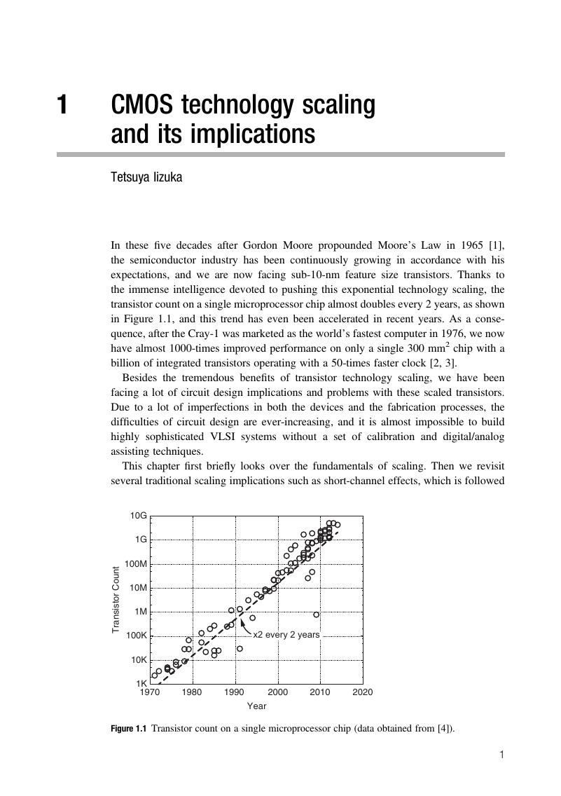
- 1 CMOS technology scaling and its implications
- 2 FinFETs: from devices to architectures
- 3 FDSOI technology and its implications for analog and digital design
- 4 Challenges and emerging trends of DSP-enabled frequency synthesizers
- 5 Digitally-assisted design of data converters
- 6 CMOS self-healing techniques for calibration and optimization of mm-wave transceivers
- 7 Analog-assisted digital design in mobile SoCs
- 8 Digitally-assisted RF design techniques
- 9 Digital controllers for switching power converters
- Appendix A
- Appendix B
- Index
- References
1 - CMOS technology scaling and its implications
Published online by Cambridge University Press: 05 August 2015
Edited by

Book contents
- Frontmatter
- Dedication
- Contents
- List of Contributors
- Preface
- 1 CMOS technology scaling and its implications
- 2 FinFETs: from devices to architectures
- 3 FDSOI technology and its implications for analog and digital design
- 4 Challenges and emerging trends of DSP-enabled frequency synthesizers
- 5 Digitally-assisted design of data converters
- 6 CMOS self-healing techniques for calibration and optimization of mm-wave transceivers
- 7 Analog-assisted digital design in mobile SoCs
- 8 Digitally-assisted RF design techniques
- 9 Digital controllers for switching power converters
- Appendix A
- Appendix B
- Index
- References
Summary
A summary is not available for this content so a preview has been provided. Please use the Get access link above for information on how to access this content.
- Type
- Chapter
- Information
- Publisher: Cambridge University PressPrint publication year: 2015
References
[1] , “Cramming more components onto integrated circuits,” Electronics, vol. 38, no. 8, 1965.Google Scholar
[2] , “The CRAY-1 computer system,” Communications of the ACM, vol. 21, no. 1, 1978.CrossRefGoogle Scholar
[3] , “Computing's energy problem: (and what we can do about it),” in IEEE International Solid-State Circuits Conference Digest of Technical Papers, pp. 10–14, 2014.
[4]Wikipedia. Transistor count [online]. Available at: http://en.wikipedia.org/wiki/Transistor_count.
[5] , , , , , and , “Design of ion-implanted MOSFET's with very small physical dimensions,” IEEE Journal of Solid-State Circuits, vol. SC-9, no. 5, 1974.CrossRefGoogle Scholar
[7] , , et al., “RF CMOS technology scaling in high-k/metal gate era for RF SoC (system-on-chip) applications,” in IEEE International Electron Devices Meeting Digest of Technical Papers, pp. 27.2.1–27.2.4, 2010.
[8] , , et al., “Advanced modeling and optimization of high performance 32nm HKMG SOI CMOS for RF/analog SoC applications,” in IEEE Symposium on VLSI Technology Digest of Technical Papers, pp. 135–136, 2012.
[9] , , et al., “A 45nm low power system-on-chip technology with dual gate (logic and I/O) high-k/metal gate strained silicon transistors,” in IEEE International Electron Devices Meeting Digest of Technical Papers, pp. 637–640, 2008.
[10] , , et al., “A 65nm CMOS SOC technology featuring strained silicon transistors for RF applications,” in IEEE International Electron Devices Meeting Digest of Technical Papers, pp. 1–3, 2006.
[11] , , , , and , “Scalability of SOI CMOS technology and circuit to millimeter wave performance,” in Proceedings of IEEE Compound Semiconductor Integrated Circuit Symposium, 2005.
[12] , , et al., “A comparison of state-of-the-art NMOS and SiGe HBT devices for analog/mixed-signal/RF circuit applications,” in IEEE Symposium on VLSI Technology Digest of Technical Papers, pp. 224–225, 2004.
[13]International Technology Roadmap for Semiconductors [online]. Available at: http://public.itrs.net.
[15] , “Roadmap for 22nm and beyond,” Microelectronic Engineering, vol. 86, no. 7–9, July, 2009.CrossRefGoogle Scholar
[16] , “Modulation of space-charge-limited current flow in insulated-gate field-effect tetrodes,” IEEE Transactions on Electron Devices, vol. ED-16, no. 9, Sep., 1969.CrossRefGoogle Scholar
[17] , “VLSI limitations from drain-induced barrier lowering,” IEEE Transactions on Electron Devices, vol. ED-26, no. 4, Sep., 1979.CrossRefGoogle Scholar
[18] , , , , , and , “Scaling the MOS transistor below 0.1μm: methodology, device structures, and technology requirements,” IEEE Transactions on Electron Devices, vol. 41, no. 6, Sep., 1994.CrossRefGoogle Scholar
[19] , , et al., “High performance fully-depleted tri-gate CMOS transistors,” IEEE Electron Device Letters, vol. 24, no. 4, Apr., 2003.CrossRefGoogle Scholar
[20] , , et al., “High-performance fully depleted silicon nanowire (diameter ≤ 5nm) gate-all-around CMOS devices,” IEEE Electron Device Letters, vol. 27, no. 5, May, 2006.CrossRefGoogle Scholar
[21] , , et al., “Polarity control in double-gate, gate-all-around vertically stacked silicon nanowire FETs,” in IEEE International Electron Devices Meeting Digest of Technical Papers, pp. 8.4.1–8.4.4, 2012.
[22] , “Innovation: the future of silicon technology,” Semico Conference, 2004.
[23] , , et al., “Electrical characteristics of highly reliable ultrathin hafnium oxide gate dielectric,” IEEE Electron Device Letters, vol. 21, no. 4, 2000.Google Scholar
[24] , “Litho and design: Moore close than Ever,” in ACM Proceedings of International Symposium on Physical Design, pp. 149–150, 2011.
[25] , “The k3 coefficient in nonparaxial λ/NA scaling equations for resolution, depth of focus, and immersion lithography,” J. Micro/Nanolith. MEMS MOEMS, vol. 1, no. 1, pp. 7–12, Apr., 2002.CrossRefGoogle Scholar
[26] , , , and , “Feature biasing versus feature-assisted lithography – a comparison of proximity correction methods for 0.5*(λ/NA) lithography,” Proceedings of SPIE 2440, Optical/Laser Microlithography, vol. VIII, p. 150, May, 1995.Google Scholar
[27] , , and , “Improving resolution in photolithography with a phase-shifting mask,” IEEE Transactions on Electron Devices, vol. ED-23, no. 12, 1982.Google Scholar
[28] , , et al., “Beyond k1=0.25 lithography: 70-nm L/S patterning using KrF scanners,” Proceedings of SPIE 5256, 23rd Annual BACUS Symposium on Photomask Technology, Dec., 2003.
[29] and , “Extreme ultraviolet lithography: a review,” Journal of Vacuum Science & Technology B, vol. 25, no. 6, pp. 1743–1761, 2007.Google Scholar
[30] , , et al., “Electron beam lithography: resolution limits and applications,” Elsevier Applied Surface Science, vol. 164, no. 1–4, pp. 111–117, 2000.Google Scholar
[31] , , and , “Matching properties of MOS transistors,” IEEE Journal of Solid-State Circuits, vol. 24, no. 5, pp. 1433–1439, 1989.CrossRefGoogle Scholar
[32] , , and , “Experimental study of threshold voltage fluctuation due to statistical variation of channel dopant number in MOSFETs,” IEEE Transactions on Electron Devices, vol. 41, no. 11, 1994.CrossRefGoogle Scholar
[33] , , et al., “A 90nm logic technology featuring 50nm strained silicon channel transistors, 7 layers of Cu interconnects, low k ILD, and 1μm2 SRAM cell,” in IEEE International Electron Devices Meeting Digest of Technical Papers, pp. 3.2.1–3.2.4, 2002.
[34] , , et al., “Lateral ion implant straggle and mask proximity effect,” IEEE Transactions on Electron Devices, vol. 50, no. 9, 2003.CrossRefGoogle Scholar
[35] and , “A comparative study of tunneling, substrate hot-electron and channel hot-electron injection induced degradation in thin-gate MOSFETs,” in IEEE International Electron Devices Meeting Digest of Technical Papers, pp. 96–99, 1984.
[36] , , et al., “New insights in the relation between electron trap generation and the statistical properties of oxide breakdown,” IEEE Transactions on Electron Devices, vol. 45, no. 4, Apr., 1998.CrossRefGoogle Scholar
[37] and , “A comprehensive model of PMOS NBTI degradation,” Microelectronics Reliability, vol. 45, pp. 71–81, 2005.CrossRefGoogle Scholar
[38] , “NBTI: recent findings and controversial topics,” IEEE International Reliability Physics Symposium (IRPS), 2011.
[39] , , et al., “Discrete resistance switching in submicrometer silicon inversion layers: individual interface traps and low-frequency (1/f?) noise,” Physical Review Letters, vol. 52, no. 3, pp. 228–231, 1984.CrossRefGoogle Scholar
[40] , , , and , “Random telegraph noise of deep-submicrometer MOSFETs,” IEEE Transactions on Electron Devices, vol. 11, no. 2, Feb., 1990.Google Scholar
[41] , , and , “1/f and random telegraph noise in silicon metal-oxide-semiconductor field-effect transistors,” Applied Physics Letters, vol. 47, no. 11, Dec., 1985.CrossRefGoogle Scholar
- 5
- Cited by