Skip to main content Accessibility help
×
Hostname: page-component-84b7d79bbc-2l2gl Total loading time: 0 Render date: 2024-07-29T22:22:18.502Z Has data issue: false hasContentIssue false

References

Published online by Cambridge University Press:  25 March 2017

Qing Gu
Affiliation:
University of Texas, Dallas
Yeshaiahu Fainman
Affiliation:
University of California, San Diego
Get access

Summary

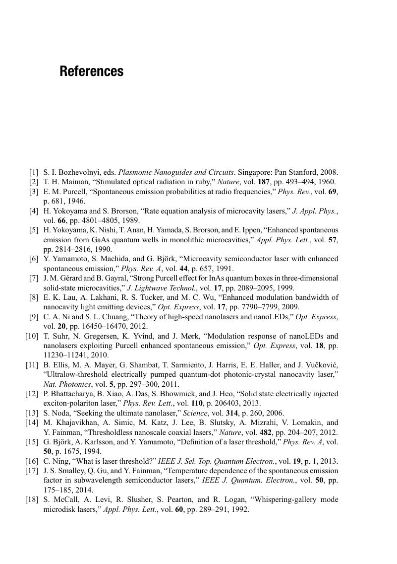
Image of the first page of this content. For PDF version, please use the ‘Save PDF’ preceeding this image.'
Type
Chapter
Information
Publisher: Cambridge University Press
Print publication year: 2017

Access options

Get access to the full version of this content by using one of the access options below. (Log in options will check for institutional or personal access. Content may require purchase if you do not have access.)

References

Bozhevolnyi, S. I., eds. Plasmonic Nanoguides and Circuits. Singapore: Pan Stanford, 2008.CrossRefGoogle Scholar
Maiman, T. H., “Stimulated optical radiation in ruby,” Nature, vol. 187, pp. 493494, 1960.CrossRefGoogle Scholar
Purcell, E. M., “Spontaneous emission probabilities at radio frequencies,” Phys. Rev., vol. 69, p. 681, 1946.Google Scholar
Yokoyama, H. and Brorson, S., “Rate equation analysis of microcavity lasers,” J. Appl. Phys., vol. 66, pp. 48014805, 1989.CrossRefGoogle Scholar
Yokoyama, H., Nishi, K., Anan, T., Yamada, H., Brorson, S., and Ippen, E., “Enhanced spontaneous emission from GaAs quantum wells in monolithic microcavities,” Appl. Phys. Lett., vol. 57, pp. 28142816, 1990.CrossRefGoogle Scholar
Yamamoto, Y., Machida, S., and Björk, G., “Microcavity semiconductor laser with enhanced spontaneous emission,” Phys. Rev. A, vol. 44, p. 657, 1991.CrossRefGoogle ScholarPubMed
Gérard, J. M. and Gayral, B., “Strong Purcell effect for InAs quantum boxes in three-dimensional solid-state microcavities,” J. Lightwave Technol., vol. 17, pp. 20892095, 1999.CrossRefGoogle Scholar
Lau, E. K., Lakhani, A., Tucker, R. S., and Wu, M. C., “Enhanced modulation bandwidth of nanocavity light emitting devices,” Opt. Express, vol. 17, pp. 77907799, 2009.CrossRefGoogle ScholarPubMed
Ni, C. A. and Chuang, S. L., “Theory of high-speed nanolasers and nanoLEDs,” Opt. Express, vol. 20, pp. 1645016470, 2012.CrossRefGoogle Scholar
Suhr, T., Gregersen, N., Yvind, K., and Mørk, J., “Modulation response of nanoLEDs and nanolasers exploiting Purcell enhanced spontaneous emission,” Opt. Express, vol. 18, pp. 1123011241, 2010.CrossRefGoogle ScholarPubMed
Ellis, B., Mayer, M. A., Shambat, G., Sarmiento, T., Harris, J., Haller, E. E., and Vučković, J., “Ultralow-threshold electrically pumped quantum-dot photonic-crystal nanocavity laser,” Nat. Photonics, vol. 5, pp. 297300, 2011.CrossRefGoogle Scholar
Bhattacharya, P., Xiao, B., Das, A., Bhowmick, S., and Heo, J., “Solid state electrically injected exciton-polariton laser,” Phys. Rev. Lett., vol. 110, p. 206403, 2013.Google ScholarPubMed
Noda, S., “Seeking the ultimate nanolaser,” Science, vol. 314, p. 260, 2006.CrossRefGoogle ScholarPubMed
Khajavikhan, M., Simic, A., Katz, M., Lee, J., Slutsky, B., Mizrahi, A., Lomakin, V., and Fainman, Y., “Thresholdless nanoscale coaxial lasers,” Nature, vol. 482, pp. 204207, 2012.CrossRefGoogle ScholarPubMed
Björk, G., Karlsson, A., and Yamamoto, Y., “Definition of a laser threshold,” Phys. Rev. A, vol. 50, p. 1675, 1994.CrossRefGoogle ScholarPubMed
Ning, C., “What is laser threshold?IEEE J. Sel. Top. Quantum Electron., vol. 19, p. 1, 2013.CrossRefGoogle Scholar
Smalley, J. S., Gu, Q., and Fainman, Y., “Temperature dependence of the spontaneous emission factor in subwavelength semiconductor lasers,” IEEE J. Quantum. Electron., vol. 50, pp. 175185, 2014.CrossRefGoogle Scholar
McCall, S., Levi, A., Slusher, R., Pearton, S., and Logan, R., “Whispering-gallery mode microdisk lasers,” Appl. Phys. Lett., vol. 60, pp. 289291, 1992.CrossRefGoogle Scholar
Gargas, D. J., Moore, M. C., Ni, A., Chang, S., Zhang, Z., Chuang, S., and Yang, P., “Whispering gallery mode lasing from zinc oxide hexagonal nanodisks,” ACS Nano, vol. 4, pp. 32703276, 2010.CrossRefGoogle ScholarPubMed
Hofrichter, J., Raz, O., Liu, L., Morthier, G., Horst, F., Regreny, P., De Vries, T., Dorren, H. J., and Offrein, B. J., “All-optical wavelength conversion using mode switching in InP microdisc laser,” Electron. Lett., vol. 47, pp. 927929, 2011.CrossRefGoogle Scholar
Song, Q., Cao, H., Ho, S., and Solomon, G., “Near-IR subwavelength microdisk lasers,” Appl. Phys. Lett., vol. 94, pp. 061109–061109–3, 2009.CrossRefGoogle Scholar
Painter, O., Lee, R., Scherer, A., Yariv, A., O’Brien, J., Dapkus, P., and Kim, I., “Two-dimensional photonic band-gap defect mode laser,” Science, vol. 284, pp. 18191821, 1999.CrossRefGoogle ScholarPubMed
Akahane, Y., Asano, T., Song, B., and Noda, S., “High-Q photonic nanocavity in a two-dimensional photonic crystal,” Nature, vol. 425, pp. 944947, 2003.CrossRefGoogle Scholar
Scofield, A. C., Kim, S., Shapiro, J. N., Lin, A., Liang, B., Scherer, A., and Huffaker, D. L., “Bottom-up photonic crystal lasers,” Nano Lett., vol. 11, pp. 53875390, 2011.CrossRefGoogle ScholarPubMed
Chen, C., Chiu, C., Chang, S., Shih, M., Kuo, M., Huang, J., Kuo, H., Chen, S., Lee, L., and Jeng, M., “Large-area ultraviolet GaN-based photonic quasicrystal laser with high-efficiency green color emission of semipolar {10–11} In 0.3 Ga 0.7 N/GaN multiple quantum wells,” Appl. Phys. Lett., vol. 102, pp. 011134–011134–4, 2013.Google Scholar
Oulton, R. F., Sorger, V. J., Zentgraf, T., Ma, R. M., Gladden, C., Dai, L., Bartal, G., and Zhang, X., “Plasmon lasers at deep subwavelength scale,” Nature, vol. 461, pp. 629632, 2009.CrossRefGoogle ScholarPubMed
Lu, Y., Kim, J., Chen, H., Wu, C., Dabidian, N., Sanders, C. E., Wang, C., Lu, M., Li, B., and Qiu, X., “Plasmonic nanolaser using epitaxially grown silver film,” Science, vol. 337, pp. 450453, 2012.CrossRefGoogle ScholarPubMed
Lin, C., Wang, J., Chen, C., Shen, K., Yeh, D., Kiang, Y., and Yang, C., “A GaN photonic crystal membrane laser,” Nanotechnology, vol. 22, p. 025201, 2011.CrossRefGoogle ScholarPubMed
Arai, S., Nishiyama, N., Maruyama, T., and Okumura, T., “GaInAsP/InP membrane lasers for optical interconnects,” IEEE J. Sel. Top. Quantum Electron., vol. 17, pp. 13811389, 2011.CrossRefGoogle Scholar
Zhou, W. and Ma, Z., “Breakthroughs in Nanomembranes and Nanomembrane Lasers,” IEEE Photon. J., vol. 5, p. 0700707, 2013.CrossRefGoogle Scholar
Wang, Z., Tian, B., and VanThourhout, D., “Design of a novel micro-laser formed by monolithic integration of a III-V pillar with a silicon photonic crystal cavity,” J. Lightwave Technol., vol. 31, pp. 14751481, 2013.CrossRefGoogle Scholar
Lin, J., Huang, Y., Yao, Q., Lv, X., Yang, Y., Xiao, J., and Du, Y., “InAlGaAs/InP cylinder microlaser connected with two waveguides,” Electron. Lett., vol. 47, pp. 929930, 2011.CrossRefGoogle Scholar
Albert, F., Hopfmann, C., Eberspacher, A., Arnold, F., Emmerling, M., Schneider, C., Hofling, S., Forchel, A., Kamp, M., and Wiersig, J., “Directional whispering gallery mode emission from Limaçon-shaped electrically pumped quantum dot micropillar lasers,” Appl. Phys. Lett., vol. 101, pp. 021116–021116–4, 2012.CrossRefGoogle Scholar
Hill, M. T., Oei, Y. S., Smalbrugge, B., Zhu, Y., De Vries, T., van Veldhoven, P. J., van Otten, F. W. M., and Eijkemans, T. J., “Lasing in metallic-coated nanocavities,” Nat. Photonics, vol. 1, pp. 589594, 2007.CrossRefGoogle Scholar
Nezhad, M. P., Simic, A., Bondarenko, O., Slutsky, B., Mizrahi, A., Feng, L., Lomakin, V., and Fainman, Y., “Room-temperature subwavelength metallo-dielectric lasers,” Nat. Photonics, vol. 4, pp. 395399, 2010.CrossRefGoogle Scholar
Lee, J. H., Khajavikhan, M., Simic, A., Gu, Q., Bondarenko, O., Slutsky, B., Nezhad, M. P., and Fainman, Y., “Electrically pumped sub-wavelength metallo-dielectric pedestal pillar lasers,” Opt. Express, vol. 19, pp. 2152421531, 2011.CrossRefGoogle ScholarPubMed
Ding, K., Hill, M., Liu, Z., Yin, L., van Veldhoven, P., and Ning, C., “Record performance of electrical injection sub-wavelength metallic-cavity semiconductor lasers at room temperature,” Opt. Express, vol. 21, pp. 47284733, 2013.CrossRefGoogle ScholarPubMed
Gu, Q., Shane, J., Vallini, F., Wingad, B., Smalley, J. S., Frateschi, N. C., and Fainman, Y., “Amorphous Al2O3 shield for thermal management in electrically pumped metallo-dielectric nanolasers,” IEEE J. Quantum. Electron., vol. 50, pp. 499509, 2014.Google Scholar
Hall, R., Fenner, G., Kingsley, J., Soltys, T., and Carlson, R., “Coherent light emission from Ga-As junctions,” Phys. Rev. Lett., vol. 9, p. 366, 1962.CrossRefGoogle Scholar
Soda, H., Iga, K., Kitahara, C., and Suematsu, Y., “GaInAsP/InP surface emitting injection lasers,” Japanese Journal of Applied Physics, vol. 18, pp. 23292330, 1979.CrossRefGoogle Scholar
Albert, F., Braun, T., Heindel, T., Schneider, C., Reitzenstein, S., Hofling, S., Worschech, L., and Forchel, A., “Whispering gallery mode lasing in electrically driven quantum dot micropillars,” Appl. Phys. Lett., vol. 97, pp. 101108–101108–3, 2010.CrossRefGoogle Scholar
Sandoghdar, V., Treussart, F., Hare, J., Lefevre-Seguin, V., Raimond, J., and Haroche, S., “Very low threshold whispering-gallery-mode microsphere laser,” Physical Review-Section A-Atomic Molecular and Optical Physics, vol. 54, p. R1777, 1996.CrossRefGoogle ScholarPubMed
Hill, M. T. and Gather, M. C., “Advances in small lasers,” Nature Photonics, vol. 8, pp. 908918, 2014.CrossRefGoogle Scholar
Nezhad, M. P., Tetz, K., and Fainman, Y., “Gain assisted propagation of surface plasmon polaritons on planar metallic waveguides,” Opt. Express, vol. 12, pp. 40724079, 2004.CrossRefGoogle ScholarPubMed
Maier, S. A., “Gain-assisted propagation of electromagnetic energy in subwavelength surface plasmon polariton gap waveguides,” Opt. Commun., vol. 258, pp. 295299, 2006.CrossRefGoogle Scholar
Bergman, D. J. and Stockman, M. I., “Surface plasmon amplification by stimulated emission of radiation: Quantum generation of coherent surface plasmons in nanosystems,” Phys. Rev. Lett., vol. 90, p. 027402, 2003.CrossRefGoogle ScholarPubMed
Ning, C., “Nanolasers: Current status of the trailblazer of synergetics.” In Self-organization in Complex Systems: The Past, Present, and Future of Synergetics. Proceedings of the International Symposium, Hanse Institute of Advanced Studies, Delmenhorst, Germany, November 13–16, pp. 190128, 2012.Google Scholar
Fainman, Y., Lee, L., Psaltis, D., and Yang, C., Optofluidics: Fundamentals, Devices, and Applications. McGraw-Hill, Inc., 2009.Google Scholar
Dang, C., Lee, J., Breen, C., Steckel, J. S., Coe-Sullivan, S., and Nurmikko, A., “Red, green and blue lasing enabled by single-exciton gain in colloidal quantum dot films,” Nat. Nanotechnol., vol. 7, pp. 335339, 2012.CrossRefGoogle ScholarPubMed
Imamog, A., Ram, R., Pau, S., and Yamamoto, Y., “Nonequilibrium condensates and lasers without inversion: Exciton-polariton lasers,” Phys. Rev. A, vol. 53, p. 4250, 1996.CrossRefGoogle Scholar
Schneider, C., Rahimi-Iman, A., Kim, N. Y., Fischer, J., Savenko, I. G., Amthor, M., Lermer, M., Wolf, A., Worschech, L., and Kulakovskii, V. D., “An electrically pumped polariton laser,” Nature, vol. 497, pp. 348352, 2013.CrossRefGoogle ScholarPubMed
Deng, H., Weihs, G., Santori, C., Bloch, J., and Yamamoto, Y., “Condensation of semiconductor microcavity exciton polaritons,” Science, vol. 298, pp. 199202, 2002.CrossRefGoogle ScholarPubMed
High, A. A., Leonard, J. R., Hammack, A. T., Fogler, M. M., Butov, L. V., Kavokin, A. V., Campman, K. L., and Gossard, A. C., “Spontaneous coherence in a cold exciton gas,” Nature, vol. 483, pp. 584588, 2012.CrossRefGoogle Scholar
Chang, S. W. and Chuang, S. L., “Fundamental formulation for plasmonic nanolasers,” IEEE J. Quantum. Electron., vol. 45, pp. 10141023, 2009.CrossRefGoogle Scholar
Li, D. and Ning, C., “Giant modal gain, amplified surface plasmon-polariton propagation, and slowing down of energy velocity in a metal-semiconductor-metal structure,” Phys. Rev. B, vol. 80, p. 153304, 2009.CrossRefGoogle Scholar
Li, D. and Ning, C., “Peculiar features of confinement factors in a metal-semiconductor waveguide,” Appl. Phys. Lett., vol. 96, p. 181109, 2010.CrossRefGoogle Scholar
Maslov, A. and Ning, C., “Reflection of guided modes in a semiconductor nanowire laser,” Appl. Phys. Lett., vol. 83, pp. 12371239, 2003.CrossRefGoogle Scholar
Moser, P., Lott, J., and Bimberg, D., “Energy efficiency of directly modulated oxide-confined high bit rate 850-nm VCSELs for optical interconnects,” IEEE J. Sel. Top. Quantum Electron., vol. 19, pp. 1702212-11702212-12, 2013.Google Scholar
Chang, S. W., Ni, C. Y. A., and Chuang, S. L., “Theory for bowtie plasmonic nanolasers,” Opt. Express, vol. 16, pp. 1058010595, 2008.CrossRefGoogle ScholarPubMed
Yariv, A., Quantum Electronics. John Wiley & Sons, 1989.Google Scholar
Iga, K., “Surface-emitting laser – its birth and generation of new optoelectronics field,” IEEE J. Sel. Top. Quantum Electron., vol. 6, pp. 12011215, 2000.CrossRefGoogle Scholar
Lee, Y., Jewell, J., Scherer, A., McCall, S., Harbison, J., and Florez, L., “Room-temperature continuous-wave vertical-cavity single-quantum-well microlaser diodes,” Electron. Lett., vol. 25, pp. 13771378, 1989.CrossRefGoogle Scholar
Lebby, M. S., Gaw, C. A., Jiang, W., Kiely, P. A., Shieh, C. L., Claisse, P. R., Ramdani, J., Hartman, D. H., Schwartz, D. B., and Grula, J., “Use of VCSEL arrays for parallel optical interconnects,” in Photonics West’96, pp. 8191, 1996.Google Scholar
Englund, D., Altug, H., Ellis, B., and Vučković, J., “Ultrafast photonic crystal lasers,” Laser & Photon. Rev., vol. 2, pp. 264274, 2008.CrossRefGoogle Scholar
Huang, M. H., Mao, S., Feick, H., Yan, H., Wu, Y., Kind, H., Weber, E., Russo, R., and Yang, P., “Room-temperature ultraviolet nanowire nanolasers,” Science, vol. 292, pp. 18971899, 2001.CrossRefGoogle ScholarPubMed
Ma, Y., Guo, X., Wu, X., Dai, L., and Tong, L., “Semiconductor nanowire lasers,” Adv. Opt. Photon., vol. 5, pp. 216273, 2013.CrossRefGoogle Scholar
Saxena, D., Mokkapati, S., Parkinson, P., Jiang, N., Gao, Q., Tan, H. H., and Jagadish, C., “Optically pumped room-temperature GaAs nanowire lasers,” Nat. Photon., vol. 7, pp. 963968, 2013.CrossRefGoogle Scholar
Alam, M. Z., Meier, J., Aitchison, J. S., and Mojahedi, M., “Super mode propagation in low index medium,” in Photonic Applications Systems Technologies Conference, pp. JThD112, 2007.CrossRefGoogle Scholar
Johnson, P. B. and Christy, R., “Optical constants of the noble metals,” Phys. Rev. B, vol. 6, p. 4370, 1972.CrossRefGoogle Scholar
Zhang, Q., Li, G., Liu, X., Qian, F., Li, Y., Sum, T. C., Lieber, C. M., and Xiong, Q., “A room temperature low-threshold ultraviolet plasmonic nanolaser,” Nat. Commun., vol. 5, 2014.CrossRefGoogle ScholarPubMed
Lu, Y., Wang, C., Kim, J., Chen, H., Lu, M., Chen, Y., Chang, W., Chen, L., Stockman, M. I., and Shih, C., “All-color plasmonic nanolasers with ultralow thresholds: Autotuning mechanism for single-mode lasing,” Nano Lett., vol. 14, pp. 43814388, 2014.CrossRefGoogle ScholarPubMed
Cao, H., Xu, J., Zhang, D., Chang, S., Ho, S., Seelig, E., Liu, X., and Chang, R., “Spatial confinement of laser light in active random media,” Phys. Rev. Lett., vol. 84, p. 5584, 2000.CrossRefGoogle ScholarPubMed
Cao, H., “Lasing in random media,” Waves in Random Media, vol. 13, pp. R1R39, 2003.CrossRefGoogle Scholar
Pickering, T., Hamm, J. M., Page, A. F., Wuestner, S., and Hess, O., “Cavity-free plasmonic nanolasing enabled by dispersionless stopped light,” Nat. Commun., vol. 5, 2014.CrossRefGoogle ScholarPubMed
Wuestner, S., Pickering, T., Hamm, J. M., Page, A. F., Pusch, A., and Hess, O., “Ultrafast dynamics of nanoplasmonic stopped-light lasing,” Faraday Discuss., vol. 178, pp. 307324, 2015.CrossRefGoogle ScholarPubMed
Hill, M. T., Marell, M., Leong, E. S., Smalbrugge, B., Zhu, Y., Sun, M., van Veldhoven, P. J., Geluk, E. J., Karouta, F., and Oei, Y., “Lasing in metal-insulator-metal sub-wavelength plasmonic waveguides,” Opt. Express, vol. 17, pp. 1110711112, 2009.CrossRefGoogle ScholarPubMed
Ding, K., Diaz, J., Bimberg, D., and Ning, C., “Modulation bandwidth and energy efficiency of metallic cavity semiconductor nanolasers with inclusion of noise effects,” Laser & Photon. Rev., vol. 9, pp. 488497, 2015.CrossRefGoogle Scholar
Agio, M. and Alù, A., Optical Antennas. Cambridge University Press, 2013.CrossRefGoogle Scholar
Yu, K., Lakhani, A., and Wu, M. C., “Subwavelength metal-optic semiconductor nanopatch lasers,” Opt. Express, vol. 18, pp. 87908799, 2010.CrossRefGoogle ScholarPubMed
Manolatou, C. and Rana, F., “Subwavelength nanopatch cavities for semiconductor plasmon lasers,” IEEE. J. Quantum. Electron., vol. 44, pp. 435447, 2008.CrossRefGoogle Scholar
Ding, Q., Mizrahi, A., Fainman, Y., and Lomakin, V., “Dielectric shielded nanoscale patch laser resonators,” Opt. Lett., vol. 36, pp. 18121814, 2011.CrossRefGoogle ScholarPubMed
Lakhani, A. M., Yu, K., and Wu, M. C., “Lasing in subwavelength semiconductor nanopatches,” Semicond. Scie.Technol., vol. 26, p. 014013, 2011.CrossRefGoogle Scholar
Ding, K., Wang, H., Hill, M. T., and Ning, C., “Design and fabrication of an electrical injection metallic bowtie plasmonic structure integrated with semiconductor gain medium,” Appl. Phys. Lett., vol. 103, p. 091112, 2013.CrossRefGoogle Scholar
Kwon, S., Kang, J., Seassal, C., Kim, S., Regreny, P., Lee, Y., Lieber, C. M., and Park, H., “Subwavelength plasmonic lasing from a semiconductor nanodisk with silver nanopan cavity,” Nano Let., vol. 10, pp. 36793683, 2010.CrossRefGoogle ScholarPubMed
Ma, R., Oulton, R. F., Sorger, V. J., Bartal, G., and Zhang, X., “Room-temperature sub-diffraction-limited plasmon laser by total internal reflection,” Nat. Mater., vol. 10, pp. 110113, 2011.CrossRefGoogle ScholarPubMed
Leymann, H., Foerster, A., Jahnke, F., Wiersig, J., and Gies, C., “Sub-and superradiance in nanolasers,” Phys. Rev. Appl., vol. 4, p. 044018, 2015.CrossRefGoogle Scholar
Stockman, M. I., “Spasers explained,” Nat. Photon., vol. 2, pp. 327329, 2008.CrossRefGoogle Scholar
Noginov, M., Zhu, G., Belgrave, A., Bakker, R., Shalaev, V., Narimanov, E., Stout, S., Herz, E., Suteewong, T., and Wiesner, U., “Demonstration of a spaser-based nanolaser,” Nature, vol. 460, pp. 11101112, 2009.CrossRefGoogle ScholarPubMed
Zheludev, N. I., Prosvirnin, S., Papasimakis, N., and Fedotov, V., “Lasing spaser,” Nature Photonics, vol. 2, pp. 351354, 2008.CrossRefGoogle Scholar
Flynn, R., Kim, C., Vurgaftman, I., Kim, M., Meyer, J., Mäkinen, A., Bussmann, K., Cheng, L., Choa, F., and Long, J., “A room-temperature semiconductor spaser operating near 1.5 μm,” Opt. Express, vol. 19, pp. 89548961, 2011.CrossRefGoogle ScholarPubMed
Suh, J. Y., Kim, C. H., Zhou, W., Huntington, M. D., Co, D. T., Wasielewski, M. R., and Odom, T. W., “Plasmonic Bowtie Nanolaser Arrays,” Nano Lett., vol. 12, pp. 57695774, 2012.CrossRefGoogle ScholarPubMed
Ginzburg, P. and Zayats, A. V., “Linewidth enhancement in spasers and plasmonic nanolasers,” Opt. Express, vol. 21, pp. 21472153, 2013.CrossRefGoogle ScholarPubMed
Dorfman, K. E., Jha, P. K., Voronine, D. V., Genevet, P., Capasso, F., and Scully, M. O., “Quantum-coherence-enhanced surface plasmon amplification by stimulated emission of radiation,” Phys. Rev. Lett., vol. 111, p. 043601, 2013.CrossRefGoogle ScholarPubMed
Meng, X., Kildishev, A. V., Fujita, K., Tanaka, K., and Shalaev, V. M., “Wavelength-tunable spasing in the visible,” Nano Lett., vol. 13, pp. 41064112, 2013.CrossRefGoogle ScholarPubMed
Rupasinghe, C., Rukhlenko, I. D., and Premaratne, M., “Spaser made of graphene and carbon nanotubes,” ACS Nano, vol. 8, pp. 24312438, 2014.CrossRefGoogle ScholarPubMed
Smotrova, E. I., Nosich, A. I., Benson, T. M., and Sewell, P., “Optical coupling of whispering-gallery modes of two identical microdisks and its effect on photonic molecule lasing,” IEEE J. Sel. Top. Quantum Electron., vol. 12, pp. 7885, 2006.CrossRefGoogle Scholar
Goebel, E., Luz, G., and Schlosser, E., “Optical gain spectra of InGaAsP/InP double heterostructures,” IEEE J. Quantum. Electron., vol. 15, pp. 697700, 1979.CrossRefGoogle Scholar
Yeh, P., Yariv, A., and Marom, E., “Theory of Bragg fiber,” J. Opt. Soc. Am., vol. 68, pp. 11961201, 1978.CrossRefGoogle Scholar
Mizrahi, A., Lomakin, V., Slutsky, B. A., Nezhad, M. P., Feng, L., and Fainman, Y., “Low threshold gain metal coated laser nanoresonators,” Opt. Lett., vol. 33, pp. 12611263, 2008.CrossRefGoogle ScholarPubMed
Smotrova, E. and Nosich, A., “Mathematical analysis of the lasing eigenvalue problem for the WG modes in a 2-D circular microcavity,” Opt. Quant. Electron., vol. 36, pp. 213221, 2004.CrossRefGoogle Scholar
Palik, E. D., Handbook of Optical Constants of Solids. New York: Academic Press, 1997.Google Scholar
Smalley, J. S., Puckett, M. W., and Fainman, Y., “Invariance of optimal composite waveguide geometries with respect to permittivity of the metal cladding,” Opt. Lett., vol. 38, pp. 51615164, 2013.CrossRefGoogle ScholarPubMed
Saleh, A. A. and Dionne, J. A., “Waveguides with a silver lining: Low threshold gain and giant modal gain in active cylindrical and coaxial plasmonic devices,” Phys. Rev. B, vol. 85, p. 045407, 2012.CrossRefGoogle Scholar
Rakić, A. D., “Algorithm for the determination of intrinsic optical constants of metal films: Application to aluminum,” Appl. Opt., vol. 34, pp. 47554767, 1995.CrossRefGoogle ScholarPubMed
McKay, J. A. and Rayne, J. A., “Temperature dependence of the infrared absorptivity of the noble metals,” Phys. Rev. B, vol. 13, p. 673, 1976.CrossRefGoogle Scholar
Kato, K. and Umemura, N., “Sellmeier equations for GaS and GaSe and their applications to the nonlinear optics in GaS x Se 1−x,” Opt. Lett., vol. 36, pp. 746747, 2011.CrossRefGoogle Scholar
Gu, Q., Slutsky, B., Vallini, F., Smalley, J. S., Nezhad, M. P., Frateschi, N. C., and Fainman, Y., “Purcell effect in sub-wavelength semiconductor lasers,” Opt. Express, vol. 21, pp. 1560315617, 2013.CrossRefGoogle ScholarPubMed
Genet, C. and Ebbesen, T., “Light in tiny holes,” Nature, vol. 445, pp. 3946, 2007.CrossRefGoogle ScholarPubMed
Stubkjaer, K., Asada, M., Arai, S., and Suematsu, Y., “Spontaneous recombination, gain and refractive index variation for 1.6 µm wavelength InGaAsP/InP lasers,” Japanese Journal of Applied Physics, vol. 20, p. 1499, 1981.CrossRefGoogle Scholar
Bennett, B. R., Soref, R. A., and del Alamo, J. A., “Carrier-induced change in refractive index of InP, GaAs and InGaAsP,” IEEE. J. Quantum. Electron., vol. 26, pp. 113122, 1990.CrossRefGoogle Scholar
Goi, A., Syassen, K., and Cardona, M., “Effect of pressure on the refractive index of Ge and GaAs,” Physical Review B, vol. 41, p. 10104, 1990.CrossRefGoogle ScholarPubMed
Rong, H., Jones, R., Liu, A., Cohen, O., Hak, D., Fang, A., and Paniccia, M., “A continuous-wave Raman silicon laser,” Nature, vol. 433, pp. 725728, 2005.CrossRefGoogle ScholarPubMed
Dal Negro, L., “Light emission from silicon nanostructures: Past, present and future perspectives,” in Lasers and Electro-Optics, 2009 and 2009 Conference on Quantum Electronics and Laser Science Conference. CLEO/QELS 2009. Conference on, 2009, pp. 12.CrossRefGoogle Scholar
Fang, A. W., Park, H., Cohen, O., Jones, R., Paniccia, M. J., and Bowers, J. E., “Electrically pumped hybrid AlGaInAs-silicon evanescent laser,” Opt. Express, vol. 14, pp. 92039210, 2006.CrossRefGoogle ScholarPubMed
Bondarenko, O., Simic, A., Gu, Q., Lee, J., Slutsky, B., Nezhad, M., and Fainman, Y., “Wafer bonded subwavelength metallo-dielectric laser,” IEEE Photon. J., p. 608, 2011.CrossRefGoogle Scholar
Niklaus, F., Kumar, R., McMahon, J., Yu, J., Lu, J., Cale, T., and Gutmann, R., “Adhesive wafer bonding using partially cured benzocyclobutene for three-dimensional integration,” J. Electrochem. Soc., vol. 153, pp. G291G295, 2006.CrossRefGoogle Scholar
Pasquariello, D. and Hjort, K., “Plasma-assisted InP-to-Si low temperature wafer bonding,” IEEE J. Sel. Top. Quantum Electron., vol. 8, pp. 118131, 2002.CrossRefGoogle Scholar
Liang, D., Bowers, J., Oakley, D., Napoleone, A., Chapman, D., Chen, C., Juodawlkis, P., and Raday, O., “High-quality 150 mm InP-to-silicon epitaxial transfer for silicon photonic integrated circuits,” Electrochem. Solid-State Lett., vol. 12, pp.H101H104, 2009.CrossRefGoogle Scholar
Liang, D., Fang, A. W., Park, H., Reynolds, T. E., Warner, K., Oakley, D. C., and Bowers, J. E., “Low-temperature, strong SiO2-SiO2 covalent wafer bonding for III–V compound semiconductors-to-silicon photonic integrated circuits,” J. Electron. Mater., vol. 37, pp. 15521559, 2008.CrossRefGoogle Scholar
Zhu, Z., Liu, H., Wang, S., Li, T., Cao, J., Ye, W., Yuan, X., and Zhu, S., “Optically pumped nanolaser based on two magnetic plasmon resonance modes,” Appl. Phys. Lett., vol. 94, p. 103106, 2009.CrossRefGoogle Scholar
Walther, H., “Experiments on cavity quantum electrodynamics,” Phys. Rep., vol. 219, pp. 263281, 1992.CrossRefGoogle Scholar
Berman, P. R., ed., Cavity Quantum Electrodynamics. San Diego, CA: Academic Press, 1994.Google Scholar
Xu, Y., Vučković, J., Lee, R., Painter, O., Scherer, A., and Yariv, A., “Finite-difference time-domain calculation of spontaneous emission lifetime in a microcavity,” J. Opt. Soc. Am. B, vol. 16, pp. 465474, 1999.CrossRefGoogle Scholar
Ryu, H. and Notomi, M., “Enhancement of spontaneous emission from the resonant modes of a photonic crystal slab single-defect cavity,” Opt. Lett., vol. 28, pp. 23902392, 2003.CrossRefGoogle ScholarPubMed
Meldrum, A., Bianucci, P., and Marsiglio, F., “Modification of ensemble emission rates and luminescence spectra for inhomogeneously broadened distributions of quantum dots coupled to optical microcavities,” Opt. Express, vol. 18, pp. 1023010246, 2010.CrossRefGoogle ScholarPubMed
Haroche, S., “New trends in atomic physics,” in Proceedings of the Les Houches Summer School of Theoretical Physics, Session XXXVIII, 1982, Grynberg, G. and Stora, R., Eds. Amsterdam: Elsevier Science, pp. 195309, 1984.Google Scholar
Suhara, T., Semiconductor Laser Fundamentals. CRC Press, 2004.CrossRefGoogle Scholar
Agrawal, G. P. and Olsson, N. A., “Self-phase modulation and spectral broadening of optical pulses in semiconductor laser amplifiers,” IEEE J. Quantum. Electron., vol. 25, pp. 22972306, 1989.CrossRefGoogle Scholar
Scully, M. O. and Zubairy, M. S., Quantum Optics. Cambridge University Press, 1997.CrossRefGoogle Scholar
Carmichael, H. J., Statistical Methods in Quantum Optics 1: Master Equations and Fokker-Planck Equations. Berlin: Springer-Verlag, 1999.CrossRefGoogle Scholar
Baba, T., Sano, D., Nozaki, K., Inoshita, K., Kuroki, Y., and Koyama, F., “Observation of fast spontaneous emission decay in GaInAsP photonic crystal point defect nanocavity at room temperature,” Appl. Phys. Lett., vol. 85, pp. 39893991, 2004.CrossRefGoogle Scholar
Iwase, H., Englund, D., and Vučković, J., “Analysis of the Purcell effect in photonic and plasmonic crystals with losses,” Opt. Express, vol. 18, pp. 1654616560, 2010.CrossRefGoogle ScholarPubMed
Asada, M., “Intraband relaxation time in quantum-well lasers,” IEEE J. Quantum. Electron., vol. 25, pp. 20192026, 1989.CrossRefGoogle Scholar
Sakurai, J. J., Modern Quantum Mechanics. Reading, MA: Addison-Wesley, 1994.Google Scholar
Fujita, M., Sakai, A., and Baba, T., “Ultrasmall and ultralow threshold GaInAsP-InP microdisk injection lasers: Design, fabrication, lasing characteristics, and spontaneous emission factor,” IEEE J. Sel. Top. Quantum Electron., vol. 5, pp. 673681, 1999.CrossRefGoogle Scholar
Altug, H., Englund, D., and Vučković, J., “Ultrafast photonic crystal nanocavity laser,” Nat. Physics, vol. 2, pp. 484488, 2006.CrossRefGoogle Scholar
Coldren, L. A. and Corzine, S. W., Diode Lasers and Photonic Integrated Circuits. New York: John Wiley & Sons, Inc., 1995.Google Scholar
Glauser, M., Rossbach, G., Cosendey, G., Levrat, J., Cobet, M., Carlin, J., Besbas, J., Gallart, M., Gilliot, P., and Butté, R., “Investigation of InGaN/GaN quantum wells for polariton laser diodes,” Phys. Status Solidi C, vol. 9, pp. 13251329, 2012.CrossRefGoogle Scholar
Yamada, M. and Suematsu, Y., “Analysis of gain suppression in undoped injection lasers,” J. Appl. Phys., vol. 52, pp. 26532664, 1981.CrossRefGoogle Scholar
Kowalsky, W., Schlachetzki, A., and Fiedler, F., “Near-band-gap absorption of InGaAsP at 1.3 μm wavelength,” Phys. Status Solidi A, vol. 68, pp. 153158, 1981.CrossRefGoogle Scholar
Groeneveld, R. H., Sprik, R., and Lagendijk, A., “Effect of a nonthermal electron distribution on the electron-phonon energy relaxation process in noble metals,” Phys. Rev. B, vol. 45, p. 5079, 1992.CrossRefGoogle ScholarPubMed
Fann, W., Storz, R., Tom, H., and Bokor, J., “Electron thermalization in gold,” Phys. Rev. B, vol. 46, p. 13592, 1992.CrossRefGoogle ScholarPubMed
Yamanishi, M. and Lee, Y., “Phase dampings of optical dipole moments and gain spectra in semiconductor lasers,” IEEE J. Quantum. Electron., vol. 23, pp. 367370, 1987.CrossRefGoogle Scholar
Chinn, S. R., Zory, P. Jr., and Reisinger, A. R., “A model for GRIN-SCH-SQW diode lasers,” IEEE J. Quantum. Electron., vol. 24, pp. 21912214, 1988.CrossRefGoogle Scholar
Yariv, A. and Yeh, P., Photonics: Optical Electronics in Modern Communications. Oxford University Press, 2007.Google Scholar
Deveaud, B., Clerot, F., Roy, N., Satzke, K., Sermage, B., and Katzer, D., “Enhanced radiative recombination of free excitons in GaAs quantum wells,” Phys. Rev. Lett., vol. 67, pp. 23552358, 1991.CrossRefGoogle ScholarPubMed
Baba, T. and Sano, D., “Low-threshold lasing and Purcell effect in microdisk lasers at room temperature,” IEEE J. Sel. Top. Quantum Electron., vol. 9, pp. 13401346, 2003.CrossRefGoogle Scholar
Chow, W. W. and Koch, S. W., Semiconductor-Laser Fundamentals. Berlin: Springer, 1999.CrossRefGoogle Scholar
Yu, P., Bhattacharya, P., and Cheng, J., “Enhanced spontaneous emission from InAs/GaAs self-organized quantum dots in a GaAs photonic-crystal-based microcavity,” J. Appl. Phys., vol. 93, pp. 61736176, 2003.CrossRefGoogle Scholar
Jahnke, F. and Koch, S., “Theory of carrier heating through injection pumping and lasing in semiconductor microcavity lasers,” Opt. Lett., vol. 18, pp. 14381440, 1993.CrossRefGoogle ScholarPubMed
Bouillard, J. G., Dickson, W., O’Connor, D. P., Wurtz, G. A., and Zayats, A. V., “Low-temperature plasmonics of metallic nanostructures,” Nano Lett., vol. 12, pp. 15611565, 2012.CrossRefGoogle ScholarPubMed
Parkins, G., Lawrence, W., and Christy, R., “Intraband optical conductivity σ (ω, T) of Cu, Ag, and Au: Contribution from electron-electron scattering,” Phys. Rev. B, vol. 23, p. 6408, 1981.CrossRefGoogle Scholar
Turhan-Sayan, G., “Temperature effects on surface plasmon resonance: Design considerations for an optical temperature sensor,” J. Lightwave Technol., vol. 21, p. 805, 2003.Google Scholar
Cassidy, D. R. and Cross, G. H., “Universal method to determine the thermo-optic coefficient of optical waveguide layer materials using a dual slab waveguide,” Appl. Phys. Lett., vol. 91, pp. 141914–141914–3, 2007.CrossRefGoogle Scholar
Della Corte, F. G., Cocorullo, G., Iodice, M., and Rendina, I., “Temperature dependence of the thermo-optic coefficient of InP, GaAs, and SiC from room temperature to 600 K at the wavelength of 1.5 μm,” Appl. Phys. Lett., vol. 77, pp. 16141616, 2000.CrossRefGoogle Scholar
Masum, J., Ramoo, D., Balkan, N., and Adams, M., “Temperature dependence of the spontaneous emission factor in VCSELs,” IEEE Proceedings – Optoelectronics, vol. 146, pp. 245251, 1999.CrossRefGoogle Scholar
Ramoo, D. M. and Adams, M. J., “Temperature dependence of the spontaneous emission factor in microcavities,” Proc. SPIE, vol. 4646, pp. 157167, 2002.CrossRefGoogle Scholar
Smalley, J. S., Gu, Q., Puckett, M. W., and Fainman, Y., “Metal-clad subwavelength semiconductor lasers with temperature-insensitive spontaneous hyper-emission,” in CLEO: Applications and Technology, pp. JTh2A. 74, 2014.CrossRefGoogle Scholar
Gies, C., Wiersig, J., Lorke, M., and Jahnke, F., “Semiconductor model for quantum-dot-based microcavity lasers,” Phys. Rev. A, vol. 75, p. 013803, 2007.CrossRefGoogle Scholar
Ritchie, R., “Plasma losses by fast electrons in thin films,” Phys. Rev., vol. 106, p. 874, 1957.CrossRefGoogle Scholar
Ozbay, E., “Plasmonics: Merging photonics and electronics at nanoscale dimensions,” Science, vol. 311, pp. 189193, 2006.CrossRefGoogle ScholarPubMed
Kittel, C., Introduction to Solid State Physics. New York: John Wiley & Sons, Inc., 2005.Google Scholar
Maier, S. A., Plasmonics: Fundamentals and Applications. Springer Science & Business Media, 2007.CrossRefGoogle Scholar
Blaber, M. G., Arnold, M. D., and Ford, M. J., “Search for the ideal plasmonic nanoshell: The effects of surface scattering and alternatives to gold and silver,” The Journal of Physical Chemistry C, vol. 113, pp. 30413045, 2009.CrossRefGoogle Scholar
Avrutsky, I., Salakhutdinov, I., Elser, J., and Podolskiy, V., “Highly confined optical modes in nanoscale metal-dielectric multilayers,” Phys. Rev. B, vol. 75, p. 241402, 2007.CrossRefGoogle Scholar
MacDonald, K. F., Sámson, Z. L., Stockman, M. I., and Zheludev, N. I., “Ultrafast active plasmonics,” Nat. Photon., vol. 3, pp. 5558, 2009.CrossRefGoogle Scholar
Pendry, J. B., “Negative refraction makes a perfect lens,” Phys. Rev. Lett., vol. 85, p. 3966, 2000.CrossRefGoogle ScholarPubMed
Ayala-Orozco, C., Urban, C., Knight, M. W., Urban, A. S., Neumann, O., Bishnoi, S. W., Mukherjee, S., Goodman, A. M., Charron, H., and Mitchell, T., “Au nanomatryoshkas as efficient near-infrared photothermal transducers for cancer treatment: Benchmarking against nanoshells,” ACS Nano, vol. 8, pp. 63726381, 2014.CrossRefGoogle ScholarPubMed
Fu, Y., Zhang, J., and Lakowicz, J. R., “Plasmonic enhancement of single-molecule fluorescence near a silver nanoparticle,” J. Fluoresc., vol. 17, pp. 811816, 2007.CrossRefGoogle Scholar
Vo-Dinh, T., Fales, A. M., Griffin, G. D., Khoury, C. G., Liu, Y., Ngo, H., Norton, S. J., Register, J. K., Wang, H., and Yuan, H., “Plasmonic nanoprobes: From chemical sensing to medical diagnostics and therapy,” Nanoscale, vol. 5, pp. 1012710140, 2013.CrossRefGoogle ScholarPubMed
Melikyan, A., Alloatti, L., Muslija, A., Hillerkuss, D., Schindler, P., Li, J., Palmer, R., Korn, D., Muehlbrandt, S., and Van Thourhout, D., “High-speed plasmonic phase modulators,” Nat. Photon., vol. 8, pp. 229233, 2014.CrossRefGoogle Scholar
O’Connor, D. and Zayats, A. V., “Data storage: The third plasmonic revolution,” Nat. Nanotechnol., vol. 5, pp. 482483, 2010.CrossRefGoogle ScholarPubMed
Lee, J., Tymchenko, M., Argyropoulos, C., Chen, P., Lu, F., Demmerle, F., Boehm, G., Amann, M., Alù, A., and Belkin, M. A., “Giant nonlinear response from plasmonic metasurfaces coupled to intersubband transitions,” Nature, vol. 511, pp. 6569, 2014.CrossRefGoogle ScholarPubMed
Galfsky, T., Krishnamoorthy, H., Newman, W., Narimanov, E., Jacob, Z., and Menon, V., “Active hyperbolic metamaterials: Enhanced spontaneous emission and light extraction,” Optica, vol. 2, pp. 6265, 2015.CrossRefGoogle Scholar
Berini, P. and De Leon, I., “Surface plasmon-polariton amplifiers and lasers,” Nat. Photon., vol. 6, pp. 1624, 2012.CrossRefGoogle Scholar
Berini, P., “Long-range surface plasmon polaritons,” Adv. Opt. Photon., vol. 1, pp. 484588, 2009.CrossRefGoogle Scholar
Plotz, G., Simon, H., and Tucciarone, J., “Enhanced total reflection with surface plasmons,” J. Opt. Soc. Am., vol. 69, pp. 419422, 1979.CrossRefGoogle Scholar
Sudarkin, A. and Demkovich, P., “Excitation of surface electromagnetic waves on the boundary of a metal with an amplifying medium,” Sov. Phys. Tech. Phys, vol. 34, p. 57, 1989.Google Scholar
Avrutsky, I., “Surface plasmons at nanoscale relief gratings between a metal and a dielectric medium with optical gain,” Phys. Rev. B, vol. 70, p. 155416, 2004.CrossRefGoogle Scholar
Tredicucci, A., Machl, C., Capasso, F., Hutchinson, A. L., Sivco, D. L., and Cho, A. Y., “Single-mode surface plasmon laser,” in Lasers and Electro-Optics, 2000. (CLEO 2000), pp. 266267.Google Scholar
Seidel, J., Grafström, S., and Eng, L., “Stimulated emission of surface plasmons at the interface between a silver film and an optically pumped dye solution,” Phys. Rev. Lett., vol. 94, p. 177401, 2005.CrossRefGoogle Scholar
De Leon, I. and Berini, P., “Theory of surface plasmon-polariton amplification in planar structures incorporating dipolar gain media,” Phys. Rev. B, vol. 78, p. 161401, 2008.CrossRefGoogle Scholar
Noginov, M., Podolskiy, V., Zhu, G., Mayy, M., Bahoura, M., Adegoke, J., Ritzo, B., and Reynolds, K., “Compensation of loss in propagating surface plasmon polariton by gain in adjacent dielectric medium,” Opt. Express, vol. 16, pp. 13851392, 2008.CrossRefGoogle ScholarPubMed
Kumar, P., Tripathi, V., and Liu, C., “A surface plasmon laser,” J. Appl. Phys., vol. 104, 2008.CrossRefGoogle Scholar
Bolger, P., Dickson, W., Krasavin, A., Liebscher, L., Hickey, S., Skryabin, D., and Zayats, A., “Amplified spontaneous emission of surface plasmon polaritons and limitations on the increase of their propagation length,” Opt. Lett., vol. 35, pp. 11971199, 2010.CrossRefGoogle ScholarPubMed
Lu, F., Li, T., Xu, J., Xie, Z., Li, L., Zhu, S., and Zhu, Y., “Surface plasmon polariton enhanced by optical parametric amplification in nonlinear hybrid waveguide,” Opt. Express, vol. 19, pp. 28582865, 2011.CrossRefGoogle ScholarPubMed
Gartia, M. R., Seo, S., Kim, J., Chang, T., Bahl, G., Lu, M., Liu, G. L., and Eden, J. G., “Injection-seeded optoplasmonic amplifier in the visible,” Sci. Rep., vol. 4, 6168, 2014.CrossRefGoogle ScholarPubMed
Economou, E., “Surface plasmons in thin films,” Phys. Rev., vol. 182, p. 539, 1969.CrossRefGoogle Scholar
Poddubny, A., Iorsh, I., Belov, P., and Kivshar, Y., “Hyperbolic metamaterials,” Nat. Photon., vol. 7, pp. 948957, 2013.CrossRefGoogle Scholar
Ni, X., Ishii, S., Thoreson, M. D., Shalaev, V. M., Han, S., Lee, S., and Kildishev, A. V., “Loss-compensated and active hyperbolic metamaterials,” Opt. Express, vol. 19, pp. 2524225254, 2011.CrossRefGoogle ScholarPubMed
Argyropoulos, C., Estakhri, N. M., Monticone, F., and Alù, A., “Negative refraction, gain and nonlinear effects in hyperbolic metamaterials,” Opt. Express, vol. 21, pp. 1503715047, 2013.CrossRefGoogle ScholarPubMed
Savelev, R. S., Shadrivov, I. V., Belov, P. A., Rosanov, N. N., Fedorov, S. V., Sukhorukov, A. A., and Kivshar, Y. S., “Loss compensation in metal-dielectric layered metamaterials,” Phys. Rev. B, vol. 87, p. 115139, 2013.CrossRefGoogle Scholar
Savelev, R., Shadrivov, I., and Kivshar, Y. S., “Wave scattering by metal-dielectric multilayer structures with gain,” JETP Letters, vol. 100, pp. 731736, 2015.CrossRefGoogle Scholar
Smalley, J. S., Vallini, F., Kanté, B., and Fainman, Y., “Modal amplification in active waveguides with hyperbolic dispersion at telecommunication frequencies,” Opt. Express, vol. 22, pp. 2108821105, 2014.CrossRefGoogle ScholarPubMed
Smalley, J. S., Vallini, F., Shahin, S., Kanté, B., and Fainman, Y., “Gain-enhanced high-k transmission through metal-semiconductor hyperbolic metamaterials,” Opt. Mater. Express, vol. 5, pp. 23002312, 2015.CrossRefGoogle Scholar
Lu, D., Kan, J. J., Fullerton, E. E., and Liu, Z., “Enhancing spontaneous emission rates of molecules using nanopatterned multilayer hyperbolic metamaterials,” Nat. Nanotechnol., vol. 9, pp. 4853, 2014.CrossRefGoogle ScholarPubMed
Popov, A. K. and Myslivets, S. A., “Transformable broad-band transparency and amplification in negative-index films,” Appl. Phys. Lett., vol. 93, p. 191117, 2008.CrossRefGoogle Scholar
Xiao, S., Drachev, V. P., Kildishev, A. V., Ni, X., Chettiar, U. K., Yuan, H., and Shalaev, V. M., “Loss-free and active optical negative-index metamaterials,” Nature, vol. 466, pp. 735738, 2010.CrossRefGoogle ScholarPubMed
Campione, S., Albani, M., and Capolino, F., “Complex modes and near-zero permittivity in 3D arrays of plasmonic nanoshells: Loss compensation using gain [Invited],” Opt. Mater. Express, vol. 1, pp. 10771089, 2011.CrossRefGoogle Scholar
Vahala, K. J., “Optical microcavities,” Nature, vol. 424, pp. 839846, 2003.CrossRefGoogle ScholarPubMed
Yokoyama, H., “Physics and device applications of optical microcavities,” Science, vol. 256, pp. 6670, 1992.CrossRefGoogle ScholarPubMed
Baida, F. I., Belkhir, A., Van Labeke, D., and Lamrous, O., “Subwavelength metallic coaxial waveguides in the optical range: Role of the plasmonic modes,” Phys. Rev. B, vol. 74, p. 205419, 2006.CrossRefGoogle Scholar
Benzaquen, R., Charbonneau, S., Sawadsky, N., Roth, A., Leonelli, R., Hobbs, L., and Knight, G., “Alloy broadening in photoluminescence spectra of Ga< inf> x</inf> In< inf> 1-x</inf> As< inf> y</inf> P< inf> 1-y</inf> lattice matched to InP,” J. Appl. Phys., vol. 75, pp. 26332639, 1994.CrossRefGoogle Scholar
Bayer, M., Reinecke, T., Weidner, F., Larionov, A., McDonald, A., and Forchel, A., “Inhibition and enhancement of the spontaneous emission of quantum dots in structured microresonators,” Phys. Rev. Lett., vol. 86, p. 3168, 2001.CrossRefGoogle ScholarPubMed
Baba, T., “Photonic crystals and microdisk cavities based on GaInAsP-InP system,” IEEE J. Sel. Top. Quantum Electron., vol. 3, pp. 808830, 1997.CrossRefGoogle Scholar
Schawlow, A. L. and Townes, C. H., “Infrared and optical masers,” Phys. Rev., vol. 112, p. 1940, 1958.CrossRefGoogle Scholar
Henry, C., “Theory of the linewidth of semiconductor lasers,” IEEE J. Quantum. Electron., vol. 18, pp. 259264, 1982.CrossRefGoogle Scholar
Bjork, G., Karlsson, A., and Yamamoto, Y., “On the linewidth of microcavity lasers,” Appl. Phys. Lett., vol. 60, pp. 304306, 1992.CrossRefGoogle Scholar
Rice, P. R. and Carmichael, H., “Photon statistics of a cavity-QED laser: A comment on the laser–phase-transition analogy,” Phys. Rev. A, vol. 50, p. 4318, 1994.CrossRefGoogle Scholar
Pedrotti, L. M., Sokol, M., and Rice, P. R., “Linewidth of four-level microcavity lasers,” Phys. Rev. A, vol. 59, p. 2295, 1999.CrossRefGoogle Scholar
Rosenzweig, M., Mohrle, M., Duser, H., and Venghaus, H., “Threshold-current analysis of InGaAs-InGaAsP multiquantum well separate-confinement lasers,” IEEE J. Quantum. Electron., vol. 27, pp. 18041811, 1991.CrossRefGoogle Scholar
Sweeney, S., Phillips, A., Adams, A., O’Reilly, E., and Thijs, P., “The effect of temperature dependent processes on the performance of 1.5-μm compressively strained InGaAs (P) MQW semiconductor diode lasers,” IEEE Photon. Technol. Lett., vol. 10, pp. 10761078, 1998.CrossRefGoogle Scholar
Sweeney, S., Jin, S., Ahmad, C., Adams, A., and Murdin, B., “Carrier recombination processes in 1.3 μm and 1.5 μm InGaAs (P)-based lasers at cryogenic temperatures and high pressures,” Physica Status Solidi (b), vol. 241, pp. 33993404, 2004.CrossRefGoogle Scholar
Fuchs, G., Schiedel, C., Hangleiter, A., Härle, V., and Scholz, F., “Auger recombination in strained and unstrained InGaAs/InGaAsP multiple quantum-well lasers,” Appl. Phys. Lett., vol. 62, pp. 396398, 1993.CrossRefGoogle Scholar
Fukuda, M., “Current drift associated with surface recombination current in InGaAsP/InP optical devices,” J. Appl. Phys., vol. 59, pp. 41724176, 1986.CrossRefGoogle Scholar
Strauf, S., Hennessy, K., Rakher, M., Choi, Y. S., Badolato, A., Andreani, L., Hu, E., Petroff, P., and Bouwmeester, D., “Self-tuned quantum dot gain in photonic crystal lasers,” Phys. Rev. Lett., vol. 96, p. 127404, 2006.CrossRefGoogle ScholarPubMed
Kinsey, N., Ferrera, M., Shalaev, V., and Boltasseva, A., “Examining nanophotonics for integrated hybrid systems: A review of plasmonic interconnects and modulators using traditional and alternative materials [Invited],” J. Opt. Soc. Am. B Optical Physics, vol. 32, p. 121, 2015.CrossRefGoogle Scholar
Balanis, C. A., Antenna Theory: Analysis and Design. New York: John Wiley & Sons, Inc., 2005.Google Scholar
Park, H. G., Kim, S. H., Kwon, S. H., Ju, Y. G., Yang, J. K., Baek, J. H., Kim, S. B., and Lee, Y. H., “Electrically driven single-cell photonic crystal laser,” Science, vol. 305, pp.14441447, 2004.CrossRefGoogle ScholarPubMed
Zhou, H., Wissinger, M., Fallert, J., Hauschild, R., Stelzl, F., Klingshirn, C., and Kalt, H., “Ordered, uniform-sized ZnO nanolaser arrays,” Appl. Phys. Lett., vol. 91, pp. 181112–181112–3, 2007.CrossRefGoogle Scholar
Hahn, C., Zhang, Z., Fu, A., Wu, C. H., Hwang, Y. J., Gargas, D. J., and Yang, P., “Epitaxial growth of InGaN nanowire arrays for light emitting diodes,” ACS Nano, vol. 5, pp. 39703976, 2011.CrossRefGoogle ScholarPubMed
Rideout, W., Sharfin, W., Koteles, E., Vassell, M., and Elman, B., “Well-barrier hole burning in quantum well lasers,” IEEE Photon. Technol. Lett., vol. 3, pp. 784786, 1991.CrossRefGoogle Scholar
Vallini, F., Gu, Q., Kats, M., Fainman, Y., and Frateschi, N. C., “Carrier saturation in multiple quantum well metallo-dielectric semiconductor nanolaser: Is bulk material a better choice for gain media?Opt. Express, vol. 21, pp. 2598525998, 2013.CrossRefGoogle ScholarPubMed
Chuang, S. L. and Chuang, S. L., Physics of Optoelectronic Devices. New York: John Wiley & Sons, Inc., 1995.Google Scholar
Reisinger, A., Zory, P. Jr., and Waters, R., “Cavity length dependence of the threshold behavior in thin quantum well semiconductor lasers,” IEEE. J. Quantum. Electron., vol. 23, pp. 993999, 1987.CrossRefGoogle Scholar
Wu, C. and Yang, E., “Physical mechanisms of carrier leakage in DH injection lasers,” J. Appl. Phys., vol. 49, pp. 31143117, 1978.CrossRefGoogle Scholar
Casey, H., “Room-temperature threshold-current dependence of GaAs-Al x Ga 1-x As double-heterostructure lasers on x and active-layer thickness,” J. Appl. Phys., vol. 49, pp. 36843692, 1978.CrossRefGoogle Scholar
Dutta, N., “Calculated temperature dependence of threshold current of GaAs-AlxGa1–xAs double heterostructure lasers,” J. Appl. Phys., vol. 52, pp. 7073, 1981.CrossRefGoogle Scholar
Lau, K. Y., “Dynamics of quantum well lasers,” in Quantum Well Lasers, Zory, P. S., Ed. New York: Academic, pp. 217276, 1993.Google Scholar
Nagarajan, R., Ishikawa, M., Fukushima, T., Geels, R. S., and Bowers, J. E., “High speed quantum-well lasers and carrier transport effects,” IEEE. J. Quantum. Electron., vol. 28, pp. 19902008, 1992.CrossRefGoogle Scholar
Cohen-Tannoudji, C., Dupont-Roc, J., and Grynberg, G., Photons and Atoms: Introduction to Quantum Electrodynamics. New York: John Wiley & Sons, Inc., 1989.Google Scholar
Lu, C., Chuang, S. L., and Bimberg, D., “Metal-cavity surface-emitting nanolasers,” IEEE. J. Quantum. Electron., vol. 49, pp. 114121, 2013.CrossRefGoogle Scholar
Shane, J., Gu, Q., Potterton, A., and Fainman, Y., “Effect of undercut etch on performance and fabrication robustness of metal-clad semiconductor nanolasers,” IEEE. J. Quantum. Electron., vol. 51, no. 1, pp. 19, 2015.CrossRefGoogle Scholar
Ding, K. and Ning, C., “Fabrication challenges of electrical injection metallic cavity semiconductor nanolasers,” Semicond. Sci. Technol., vol. 28, p. 124002, 2013.CrossRefGoogle Scholar
Chuang, S. L., Gorman, J. O., and Levi, A., “Amplified spontaneous emission and carrier pinning in laser diodes,” IEEE. J. Quantum. Electron., vol. 29, pp. 16311639, 1993.CrossRefGoogle Scholar
Ding, K. and Ning, C., “Metallic subwavelength-cavity semiconductor nanolasers,” Light: Sci. Appl., vol. 1, p. e20, 2012.CrossRefGoogle Scholar
Hess, O., Pendry, J., Maier, S., Oulton, R., Hamm, J., and Tsakmakidis, K., “Active nanoplasmonic metamaterials,” Nat. Mater., vol. 11, pp. 573584, 2012.CrossRefGoogle ScholarPubMed
Ning, C., Indik, R., and Moloney, J., “Self-consistent approach to thermal effects in vertical-cavity surface-emitting lasers,” J. Opt. Soc. Am. B, vol. 12, pp. 19932004, 1995.CrossRefGoogle Scholar
Yu, S. F., Analysis and Design of Vertical Cavity Surface Emitting Lasers. New York: Wiley-VCH, 2003.CrossRefGoogle Scholar
Yoneoka, S., Lee, J., Liger, M., Yama, G., Kodama, T., Gunji, M., Provine, J., Howe, R. T., Goodson, K. E., and Kenny, T. W., “Electrical and thermal conduction in atomic layer deposition nanobridges down to 7 nm thickness,” Nano Lett., vol. 12, pp. 683686, 2012.CrossRefGoogle ScholarPubMed
Wank, J. R., George, S. M., and Weimer, A. W., “Nanocoating individual cohesive boron nitride particles in a fluidized bed by ALD,” Powder. Technol., vol. 142, pp. 5969, 2004.CrossRefGoogle Scholar
Chen, G. and Shakouri, A., “Heat transfer in nanostructures for solid-state energy conversion,” J. Heat Transfer, vol. 124, pp. 242252, 2002.CrossRefGoogle Scholar
Green, B. M., Chu, K. K., Chumbes, E. M., Smart, J. A., Shealy, J. R., and Eastman, L. F., “The effect of surface passivation on the microwave characteristics of undoped AlGaN/GaN HEMTs,” Electron. Dev. Lett., vol. 21, pp. 268270, 2000.CrossRefGoogle Scholar
Shih, M., Bagheri, M., Mock, A., Choi, S., OBrien, J., Dapkus, P., and Kuang, W., “Identification of modes and single mode operation of sapphire-bonded photonic crystal lasers under continuous-wave room temperature operation,” Appl. Phys. Lett., vol. 90, pp. 121116–121116–3, 2007.CrossRefGoogle Scholar
Chu, S., Wang, G., Zhou, W., Lin, Y., Chernyak, L., Zhao, J., Kong, J., Li, L., Ren, J., and Liu, J., “Electrically pumped waveguide lasing from ZnO nanowires,” Nat. Nanotechnol., vol. 6, pp. 506510, 2011.CrossRefGoogle ScholarPubMed
Min, B., Lee, J. S., Cho, K., Hwang, J. W., Kim, H., Sung, M. Y., Kim, S., Park, J., Seo, H. W., and Bae, S. Y., “Semiconductor nanowires surrounded by cylindrical Al2O3 shells,” J. Electron. Mater., vol. 32, pp. 13441348, 2003.CrossRefGoogle Scholar
Lee, S. and Cahill, D. G., “Heat transport in thin dielectric films,” J. Appl. Phys., vol. 81, pp. 25902595, 1997.CrossRefGoogle Scholar
Dörre, E. and Hübner, H., Alumina: Processing, Properties, and Applications. New York: Springer-Verlag, 1984.CrossRefGoogle Scholar
Duan, X., Huang, Y., Agarwal, R., and Lieber, C. M., “Single-nanowire electrically driven lasers,” Nature, vol. 421, pp. 241245, 2003.CrossRefGoogle ScholarPubMed
Kim, M. W. and Ku, P., “Semiconductor nanoring lasers,” Appl. Phys. Lett., vol. 98, pp. 201105–201105–3, 2011.CrossRefGoogle Scholar
Yang, H., Zhao, D., Chuwongin, S., Seo, J., Yang, W., Shuai, Y., Berggren, J., Hammar, M., Ma, Z., and Zhou, W., “Transfer-printed stacked nanomembrane lasers on silicon,” Nat. Photon., vol. 6, pp. 617622, 2012.CrossRefGoogle Scholar
Chen, K. J. and Huang, S., “AlN passivation by plasma-enhanced atomic layer deposition for GaN-based power switches and power amplifiers,” Semicond. Sci. Technol., vol. 28, pp. 074015–1074015–8, 2013.CrossRefGoogle Scholar
Kleiner, M. B., Kühn, S., and Weber, W., “Thermal conductivity measurements of thin silicon dioxide films in integrated circuits,” IEEE Trans. Electron Dev., vol. 43, pp. 16021609, 1996.CrossRefGoogle Scholar
Bosund, M., Sajavaara, T., Laitinen, M., Huhtio, T., Putkonen, M., Airaksinen, V., and Lipsanen, H., “Properties of AlN grown by plasma enhanced atomic layer deposition,” Appl. Surf. Sci., vol. 257, pp. 78277830, 2011.CrossRefGoogle Scholar
Matsudaira, A., Lu, C., Zhang, M., Chuang, S. L., Stock, E., and Bimberg, D., “Cavity-volume scaling law of quantum-dot metal-cavity surface-emitting microlasers,” IEEE Photon. J., vol. 4, pp. 11031114, 2012.CrossRefGoogle Scholar
Forchel, A., Menschig, A., Maile, B., Leier, H., and Germann, R., “Transport and optical properties of semiconductor quantum wires,” J. Vac. Sci. Technol. B, vol. 9, pp. 444450, 1991.CrossRefGoogle Scholar
Cahill, D. G., “Thermal conductivity measurement from 30 to 750 K: The 3 ω method,” Rev. Sci. Instrum., vol. 61, pp. 802808, 1990.CrossRefGoogle Scholar
Shin, S., Cho, H. N., Kim, B. S., and Cho, H. H., “Influence of upper layer on measuring thermal conductivity of multilayer thin films using differential 3-ω method,” Thin Solid Films, vol. 517, pp. 933936, 2008.CrossRefGoogle Scholar
Kwon, M. and Shin, S., “Simple and fast numerical analysis of multilayer waveguide modes,” Opt. Commun., vol. 233, pp. 119126, 2004.CrossRefGoogle Scholar
Tsakmakidis, K. L., Pickering, T. W., Hamm, J. M., Page, A. F., and Hess, O., “Completely stopped and dispersionless light in plasmonic waveguides,” Phys. Rev. Lett., vol. 112, p. 167401, 2014.CrossRefGoogle ScholarPubMed
Baba, T., “Slow light in photonic crystals,” Nature Photonics, vol. 2, pp. 465473, 2008.CrossRefGoogle Scholar
Mookherjea, S., Park, J. S., Yang, S., and Bandaru, P. R., “Localization in silicon nanophotonic slow-light waveguides,” Nature Photonics, vol. 2, pp. 9093, 2008.CrossRefGoogle Scholar
Imamoğlu, A. and Ram, R., “Semiconductor lasers without population inversion,” Opt. Lett., vol. 19, pp. 17441746, 1994.CrossRefGoogle ScholarPubMed
Deng, H., Haug, H., and Yamamoto, Y., “Exciton-polariton bose-einstein condensation,” Reviews of Modern Physics, vol. 82, p. 1489, 2010.CrossRefGoogle Scholar
Kasprzak, J., Richard, M., Kundermann, S., Baas, A., Jeambrun, P., Keeling, J., Marchetti, F., Szymańska, M., Andre, R., and Staehli, J., “Bose–Einstein condensation of exciton polaritons,” Nature, vol. 443, pp. 409414, 2006.CrossRefGoogle ScholarPubMed
Yamamoto, Y., Tassone, F., and Cao, H., Semiconductor Cavity Quantum Electrodynamics. Springer Science & Business Media, 2000.Google Scholar
Yoshie, T., Scherer, A., Hendrickson, J., Khitrova, G., Gibbs, H., Rupper, G., Ell, C., Shchekin, O., and Deppe, D., “Vacuum Rabi splitting with a single quantum dot in a photonic crystal nanocavity,” Nature, vol. 432, pp. 200203, 2004.CrossRefGoogle Scholar
Weisbuch, C., Nishioka, M., Ishikawa, A., and Arakawa, Y., “Observation of the coupled exciton-photon mode splitting in a semiconductor quantum microcavity,” Phys. Rev. Lett., vol. 69, p. 3314, 1992.CrossRefGoogle Scholar
Tassone, F., Bassani, F., and Andreani, L., “Quantum-well reflectivity and exciton-polariton dispersion,” Physical Review B, vol. 45, p. 6023, 1992.CrossRefGoogle ScholarPubMed
Keldysh, L. and Kozlov, A., “Collective properties of excitons in semiconductors,” Sov. Phys.JETP, vol. 27, p. 521, 1968.Google Scholar
Keldysh, L. and Kopaev, Y. V., “Possible instability of semimetallic state toward coulomb interaction,” Soviet Physics Solid State, USSR, vol. 6, pp. 2219-&, 1965.Google Scholar
Imamoḡlu, A. and Ram, R., “Quantum dynamics of exciton lasers,” Phys. Lett. A, vol. 214, pp. 193198, 1996.CrossRefGoogle Scholar
Lagoudakis, P., Martin, M., Baumberg, J., Qarry, A., Cohen, E., and Pfeiffer, L., “Electron-polariton scattering in semiconductor microcavities,” Phys. Rev. Lett., vol. 90, p. 206401, 2003.CrossRefGoogle ScholarPubMed
Bhattacharya, P., Frost, T., Deshpande, S., Baten, M. Z., Hazari, A., and Das, A., “Room temperature electrically injected polariton laser,” Phys. Rev. Lett., vol. 112, p. 236802, 2014.CrossRefGoogle ScholarPubMed
Igarashi, K., Takeshima, K., Tsuritani, T., Takahashi, H., Sumita, S., Morita, I., Tsuchida, Y., Tadakuma, M., Maeda, K., and Saito, T., “110.9-Tbit/s SDM transmission over 6,370 km using a full C-band seven-core EDFA,” Opt. Express, vol. 21, pp. 1805318060, 2013.CrossRefGoogle Scholar
Morioka, T., Awaji, Y., Ryf, R., Winzer, P., Richardson, D., and Poletti, F., “Enhancing optical communications with brand new fibers,” IEEE Communications Magazine, vol. 50, pp. s31s42, 2012.CrossRefGoogle Scholar
Poletti, F., Wheeler, N., Petrovich, M., Baddela, N., Fokoua, E. N., Hayes, J., Gray, D., Li, Z., Slavík, R., and Richardson, D., “Towards high-capacity fibre-optic communications at the speed of light in vacuum,” Nat. Photon., vol. 7, pp. 279284, 2013.CrossRefGoogle Scholar
Luo, L., Ophir, N., Chen, C. P., Gabrielli, L. H., Poitras, C. B., Bergmen, K., and Lipson, M., “WDM-compatible mode-division multiplexing on a silicon chip,” Nat. Commun., vol. 5, 2014.CrossRefGoogle ScholarPubMed
Horst, F., Green, W. M., Assefa, S., Shank, S. M., Vlasov, Y. A., and Offrein, B. J., “Cascaded Mach-Zehnder wavelength filters in silicon photonics for low loss and flat pass-band WDM (de-) multiplexing,” Opt. Express, vol. 21, pp. 1165211658, 2013.CrossRefGoogle ScholarPubMed
Assefa, S., Shank, S., Green, W., Khater, M., Kiewra, E., Reinholm, C., Kamlapurkar, S., Rylyakov, A., Schow, C., and Horst, F., “A 90 nm CMOS integrated nano-photonics technology for 25Gbps WDM optical communications applications,” in IEEE International Electron Devices Meeting (IEDM), 2012, pp. 3133.38.CrossRefGoogle Scholar
Marchena, E., Creazzo, T., Krasulick, S. B., Yu, P., Van Orden, D., Spann, J. Y., Blivin, C. C., Dallesasse, J. M., Varangis, P., and Stone, R. J., “Integrated tunable CMOS laser for si photonics,” in National Fiber Optic Engineers Conference, 2013, pp. PDP5 C. 7.CrossRefGoogle Scholar
Roelkens, G., Liu, L., Liang, D., Jones, R., Fang, A., Koch, B., and Bowers, J., “III-V/silicon photonics for on-chip and intra-chip optical interconnects,” Laser & Photon. Rev., vol. 4, pp. 751779, 2010.CrossRefGoogle Scholar
Reed, G. T., Mashanovich, G., Gardes, F., and Thomson, D., “Silicon optical modulators,” Nat. Photon., vol. 4, pp. 518526, 2010.CrossRefGoogle Scholar
Casalino, M., Iodice, M., Sirleto, L., Rendina, I., and Coppola, G., “Asymmetric MSM sub-bandgap all-silicon photodetector with low dark current,” Opt. Express, vol. 21, pp. 2807228082, 2013.CrossRefGoogle ScholarPubMed
Huang, S., Lu, W., Li, C., Huang, W., Lai, H., and Chen, S., “A CMOS-compatible approach to fabricate an ultra-thin germanium-on-insulator with large tensile strain for Si-based light emission,” Opt. Express, vol. 21, pp. 640646, 2013.CrossRefGoogle ScholarPubMed
Pospischil, A., Humer, M., Furchi, M. M., Bachmann, D., Guider, R., Fromherz, T., and Mueller, T., “CMOS-compatible graphene photodetector covering all optical communication bands,” Nat. Photon., vol. 7, pp. 892896, 2013.CrossRefGoogle Scholar
Boyraz, O. and Jalali, B., “Demonstration of directly modulated silicon Raman laser,” Opt. Express, vol. 13, pp. 796800, 2005.CrossRefGoogle ScholarPubMed
Camacho-Aguilera, R. E., Cai, Y., Patel, N., Bessette, J. T., Romagnoli, M., Kimerling, L. C., and Michel, J., “An electrically pumped germanium laser,” Opt. Express, vol. 20, pp. 1131611320, 2012.CrossRefGoogle ScholarPubMed
Tanaka, S., Jeong, S., Sekiguchi, S., Kurahashi, T., Tanaka, Y., and Morito, K., “High-output-power, single-wavelength silicon hybrid laser using precise flip-chip bonding technology,” Opt. Express, vol. 20, pp. 2805728069, 2012.CrossRefGoogle ScholarPubMed
Zilkie, A., Seddighian, P., Bijlani, B., Qian, W., Lee, D., Fathololoumi, S., Fong, J., Shafiiha, R., Feng, D., and Luff, B., “Power-efficient III-V/Silicon external cavity DBR lasers,” Opt. Express, vol. 20, pp. 2345623462, 2012.CrossRefGoogle ScholarPubMed
Lee, J. H., Shubin, I., Yao, J., Bickford, J., Luo, Y., Lin, S., Djordjevic, S. S., Thacker, H. D., Cunningham, J. E., and Raj, K., “High power and widely tunable Si hybrid external-cavity laser for power efficient Si photonics WDM links,” Opt. Express, vol. 22, pp. 76787685, 2014.CrossRefGoogle ScholarPubMed
Hsu, C., Chen, Y., and Su, Y., “Heteroepitaxy for GaAs on nanopatterned Si (001),” IEEE Photon. Technol. Lett., vol. 24, pp. 10091011, 2012.CrossRefGoogle Scholar
Chen, R., Tran, T. D., Ng, K. W., Ko, W. S., Chuang, L. C., Sedgwick, F. G., and Chang-Hasnain, C., “Nanolasers grown on silicon,” Nat. Photon., vol. 5, pp. 170175, 2011.CrossRefGoogle Scholar
Rojo Romeo, P., Van Campenhout, J., Regreny, P., Kazmierczak, A., Seassal, C., Letartre, X., Hollinger, G., Van Thourhout, D., Baets, R., and Fedeli, J., “Heterogeneous integration of electrically driven microdisk based laser sources for optical interconnects and photonic ICs,” Opt. Express, vol. 14, pp. 38643871, 2006.CrossRefGoogle ScholarPubMed
Fang, A. W., Lively, E., Kuo, Y., Liang, D., and Bowers, J. E., “A distributed feedback silicon evanescent laser,” Opt. Express, vol. 16, pp. 44134419, 2008.CrossRefGoogle ScholarPubMed
Stanković, S., Jones, R., Sysak, M. N., Heck, J. M., Roelkens, G., and Van Thourhout, D., “Hybrid III–V/Si distributed-feedback laser based on adhesive bonding,” IEEE Photon. Technol. Lett., vol. 24, pp. 21552158, 2012.CrossRefGoogle Scholar
Keyvaninia, S., Roelkens, G., Van Thourhout, D., Jany, C., Lamponi, M., Le Liepvre, A., Lelarge, F., Make, D., Duan, G., and Bordel, D., “Demonstration of a heterogeneously integrated III-V/SOI single wavelength tunable laser,” Opt. Express, vol. 21, pp. 37843792, 2013.CrossRefGoogle ScholarPubMed
Tao, L., Yuan, L., Li, Y., Yu, H., Wang, B., Kan, Q., Chen, W., Pan, J., Ran, G., and Wang, W., “4-λ InGaAsP-Si distributed feedback evanescent lasers with varying silicon waveguide width,” Opt. Express, vol. 22, pp. 54485454, 2014.CrossRefGoogle ScholarPubMed
Bondarenko, O., Gu, Q., Shane, J., Simic, A., Slutsky, B., and Fainman, Y., “Wafer bonded distributed feedback laser with sidewall modulated Bragg gratings,” Appl. Phys. Lett., vol. 103, pp. 043105–043105–4, 2013.CrossRefGoogle Scholar
De Koninck, Y., Raineri, F., Bazin, A., Raj, R., Roelkens, G., and Baets, R., “Experimental demonstration of a hybrid III–V-on-silicon microlaser based on resonant grating cavity mirrors,” Opt. Lett., vol. 38, pp. 24962498, 2013.CrossRefGoogle ScholarPubMed
Zhang, Y., Qu, H., Wang, H., Zhang, S., Liu, L., Ma, S., and Zheng, W., “A hybrid silicon single mode laser with a slotted feedback structure,” Opt. Express, vol. 21, pp. 877883, 2013.CrossRefGoogle ScholarPubMed
Santis, C. T., Steger, S. T., Vilenchik, Y., Vasilyev, A., and Yariv, A., “High-coherence semiconductor lasers based on integral high-Q resonators in hybrid Si/III-V platforms,” Proc. Natl. Acad. Sci. U. S. A., vol. 111, pp. 28792884, 2014.CrossRefGoogle ScholarPubMed
Gu, Q., Smalley, J. S., Nezhad, M. P., Simic, A., Lee, J. H., Katz, M., Bondarenko, O., Slutsky, B., Mizrahi, A., Lomakin, V., and Fainman, Y., “Subwavelength semiconductor lasers for dense chip-scale integration,” Adv. Opt. Photon., vol. 6, pp. 156, 2014.CrossRefGoogle Scholar
Kim, M., Li, Z., Huang, K., Going, R., Wu, M. C., and Choo, H., “Engineering of metal-clad optical nanocavity to optimize coupling with integrated waveguides,” Opt. Express, vol. 21, pp. 2579625804, 2013.CrossRefGoogle ScholarPubMed
Kim, M., Lakhani, A. M., and Wu, M. C., “Efficient waveguide-coupling of metal-clad nanolaser cavities,” Opt. Express, vol. 19, pp. 2350423512, 2011.CrossRefGoogle ScholarPubMed
Haus, H. A., Waves and Fields in Optoelectronics (Prentice-Hall series in solid state physical electronics). Englewood Cliffs, NJ: Prentice Hall, 1984.Google Scholar
Lau, E. K., Zhao, X., Sung, H., Parekh, D., Chang-Hasnain, C., and Wu, M. C., “Strong optical injection-locked semiconductor lasers demonstrating ˃ 100-GHz resonance frequencies and 80-GHz intrinsic bandwidths,” Opt. Express, vol. 16, pp. 66096618, 2008.CrossRefGoogle ScholarPubMed
Matsui, Y., Murai, H., Arahira, S., Ogawa, Y. and Suzuki, A., “Enhanced modulation bandwidth for strain-compensated InGaAlAs-InGaAsP MQW lasers,” IEEE. J. Quantum. Electron., vol. 34, pp. 19701978, 1998.CrossRefGoogle Scholar
Ledentsov, N., Bimberg, D., Hopfer, F., Mutig, A., Shchukin, V., Savel’ev, A., Fiol, G., Stock, E., Eisele, H., and Dähne, M., “Submonolayer quantum dots for high speed surface emitting lasers,” Nanoscale Res. Lett., vol. 2, pp. 417429, 2007.CrossRefGoogle ScholarPubMed
Moser, P., Lott, J., Wolf, P., Larisch, G., Li, H., and Bimberg, D., “85-fJ dissipated energy per bit at 30 Gb/s across 500-m multimode fiber using 850-nm VCSELs,” IEEE Photon. Technol. Lett., vol. 25, pp. 16381641, 2013.CrossRefGoogle Scholar
Yamanishi, M. and Suemune, I., “Comment on polarization dependent momentum matrix elements in quantum well lasers,” Jpn. J. Appl. Phys., vol. 23, p. L35, 1984.CrossRefGoogle Scholar
Bondarenko, O., Fang, C., Vallini, F., Smalley, J. S., and Fainman, Y., “Extremely compact hybrid III-V/SOI lasers: Design and fabrication approaches,” Opt. Express, vol. 23, pp. 26962712, 2015.CrossRefGoogle ScholarPubMed
Kogelnik, H. and Shank, C., “Coupled-wave theory of distributed feedback lasers,” J. Appl. Phys., vol. 43, pp. 23272335, 1972.CrossRefGoogle Scholar
Morthier, G. and Vankwikelberge, P., Handbook of Distributed Feedback Laser Diodes. Boston: Artech House, 2013.Google Scholar
Grieco, A., Slutsky, B., and Fainman, Y., “Characterization of waveguide loss using distributed Bragg reflectors,” Appl. Phys. B, vol. 114, pp. 467474, 2014.CrossRefGoogle Scholar
Roelkens, G., Van Thourhout, D., Baets, R., and Smit, M., “Laser emission and photodetection in an InP/InGaAsP layer integrated on and coupled to a Silicon-on-Insulator waveguide circuit,” Opt. Express, vol. 14, pp. 81548159, 2006.CrossRefGoogle Scholar
Heck, M., Bauters, J. F., Davenport, M. L., Doylend, J. K., Jain, S., Kurczveil, G., Srinivasan, S., Tang, Y., and Bowers, J. E., “Hybrid silicon photonic integrated circuit technology,” IEEE J. Sel. Top. Quantum Electron., vol. 19, 2013.CrossRefGoogle Scholar
Duan, G., Jany, C., Le Liepvre, A., Accard, A., Lamponi, M., Make, D., Kaspar, P., Levaufre, G., Girard, N., and Lelarge, F., “Hybrid III–V on silicon lasers for photonic integrated circuits on silicon,” IEEE J. Sel. Top. Quantum Electron., vol. 20, pp. 158170, 2014.CrossRefGoogle Scholar
Agrawal, G. P. and Dutta, N. K., Long Wavelength Semiconductor Lasers. New York: Van Nostrand Reinhold, 1986.CrossRefGoogle Scholar
Lamponi, M., Keyvaninia, S., Jany, C., Poingt, F., Lelarge, F., De Valicourt, G., Roelkens, G., Van Thourhout, D., Messaoudene, S., and Fedeli, J., “Low-threshold heterogeneously integrated InP/SOI lasers with a double adiabatic taper coupler,” IEEE Photon. Technol. Lett., vol. 24, pp. 7678, 2012.CrossRefGoogle Scholar
Park, H., Kuo, Y., Fang, A. W., Jones, R., Cohen, O., Paniccia, M. J., and Bowers, J. E., “A hybrid AlGaInAs-silicon evanescent preamplifier and photodetector,” Opt. Express, vol. 15, pp. 1353913546, 2007.CrossRefGoogle ScholarPubMed
Kurczveil, G., Heck, M. J., Peters, J. D., Garcia, J. M., Spencer, D., and Bowers, J. E., “An integrated hybrid silicon multiwavelength AWG laser,” IEEE J. Sel. Top. Quantum Electron., vol. 17, pp. 15211527, 2011.CrossRefGoogle Scholar
Koyanagi, M., Nakamura, T., Yamada, Y., Kikuchi, H., Fukushima, T., Tanaka, T., and Kurino, H., “Three-dimensional integration technology based on wafer bonding with vertical buried interconnections,” IEEE Trans. Electron Dev., vol. 53, pp. 27992808, 2006.CrossRefGoogle Scholar
de Valicourt, G., Le Liepvre, A., Vacondio, F., Simonneau, C., Lamponi, M., Jany, C., Accard, A., Lelarge, F., Make, D., and Poingt, F., “Directly modulated and fully tunable hybrid silicon lasers for future generation of coherent colorless ONU,” Opt. Express, vol. 20, pp.B552B557, 2012.CrossRefGoogle ScholarPubMed
Cortes, C., Newman, W., Molesky, S., and Jacob, Z., “Quantum nanophotonics using hyperbolic metamaterials,” J. Opt., vol. 14, p. 063001, 2012.CrossRefGoogle Scholar
Ramakrishna, S. A. and Pendry, J. B., “Removal of absorption and increase in resolution in a near-field lens via optical gain,” Phys. Rev. B, vol. 67, p. 201101, 2003.CrossRefGoogle Scholar
Ohring, M., Materials Science of Thin Films. San Diego, CA: Academic Press, 2001.Google Scholar
George, S. M., “Atomic layer deposition: An overview,” Chem. Rev., vol. 110, pp. 111131, 2009.CrossRefGoogle Scholar
Hämäläinen, J., Ritala, M., and Leskelä, M., “Atomic layer deposition of noble metals and their oxides,” Chem. Mater., vol. 26, pp. 786801, 2013.CrossRefGoogle Scholar
Chang, S., Lin, T., and Chuang, S. L., “Theory of plasmonic Fabry-Perot nanolasers,” Opt. Express, vol. 18, pp. 1503915053, 2010.CrossRefGoogle ScholarPubMed
Altug, H. and Vuckovic, J., “Photonic crystal nanocavity array laser,” Opt. Express, vol. 13, pp. 88198828, 2005.CrossRefGoogle ScholarPubMed
Morris, S. M., Hands, P. J., Findeisen-Tandel, S., Cole, R. H., Wilkinson, T. D., and Coles, H. J., “Polychromatic liquid crystal laser arrays towards display applications,” Opt. Express, vol. 16, pp. 1882718837, 2008.CrossRefGoogle ScholarPubMed
Zhou, W., Dridi, M., Suh, J. Y., Kim, C. H., Wasielewski, M. R., Schatz, G. C., and Odom, T. W., “Lasing action in strongly coupled plasmonic nanocavity arrays,” Nat. Nanotechnol., vol. 8, no. 7, pp. 506511, 2013.CrossRefGoogle ScholarPubMed
Abe, H., Narimatsu, M., Kita, S., Tomitaka, A., Takemura, Y., and Baba, T., “Live cell imaging using photonic crystal nanolaser array,” Micro-TAS, vol. 593, p. 2011, 2011.Google Scholar
Sun, J., Timurdogan, E., Yaacobi, A., Hosseini, E. S., and Watts, M. R., “Large-scale nanophotonic phased array,” Nature, vol. 493, pp. 195199, 2013.CrossRefGoogle ScholarPubMed
Oclaro, “Data Sheet: 850 nm 20Gb/s Multimode VCSEL Chip Array,” <www.oclaro.com/datasheets/D00473-PB%20APA7601xy0000%20Datasheet%20Iss01.pdf>>Google Scholar
He, L., Özdemir, Ş. K., Zhu, J., Kim, W., and Yang, L., “Detecting single viruses and nanoparticles using whispering gallery microlasers,” Nat. Nanotechnol., vol. 6, pp. 428432, 2011.CrossRefGoogle ScholarPubMed
Francois, A. and Himmelhaus, M., “Whispering gallery mode biosensor operated in the stimulated emission regime,” Appl. Phys. Lett., vol. 94, p. 031101, 2009.CrossRefGoogle Scholar
Gather, M. C. and Yun, S. H., “Single-cell biological lasers,” Nat. Photon., vol. 5, pp. 406410, 2011.CrossRefGoogle Scholar
Gather, M. C. and Yun, S. H., “Lasing from Escherichia coli bacteria genetically programmed to express green fluorescent protein,” Opt. Lett., vol. 36, pp. 32993301, 2011.CrossRefGoogle ScholarPubMed
Nizamoglu, S., Gather, M. C., and Yun, S. H., “All-Biomaterial Laser Using Vitamin and Biopolymers,” Adv. Mater., vol. 25, pp. 59435947, 2013.CrossRefGoogle ScholarPubMed
Sun, Y., Shopova, S. I., Wu, C. S., Arnold, S., and Fan, X., “Bioinspired optofluidic FRET lasers via DNA scaffolds,” Proc. Natl. Acad. Sci. U. S. A., vol. 107, pp.1603916042, 2010.CrossRefGoogle ScholarPubMed
Glauber, R. J. and Lewenstein, M., “Quantum optics of dielectric media,” Phys. Rev. A, vol. 43, p. 467, 1991.CrossRefGoogle ScholarPubMed
Chang, S. W. and Chuang, S. L., “Normal modes for plasmonic nanolasers with dispersive and inhomogeneous media,” Opt. Lett., vol. 34, pp. 9193, 2009.CrossRefGoogle ScholarPubMed
Glauber, R. J., “Optical coherence and photon statistics,” in Quantum Optics and Electronics, DeWitt, C. et al., Eds. New York: Gordon and Breach, p. 63, 1965,Google Scholar
Björk, G., Machida, S., Yamamoto, Y., and Igeta, K., “Modification of spontaneous emission rate in planar dielectric microcavity structures,” Phys. Rev. A, vol. 44, p. 669, 1991.CrossRefGoogle ScholarPubMed
Srinivasan, K. and Painter, O., “Linear and nonlinear optical spectroscopy of a strongly coupled microdisk–quantum dot system,” Nature, vol. 450, pp. 862865, 2007.CrossRefGoogle ScholarPubMed
Khitrova, G., Gibbs, H., Kira, M., Koch, S., and Scherer, A., “Vacuum Rabi splitting in semiconductors,” Nat. Phys., vol. 2, pp. 8190, 2006.CrossRefGoogle Scholar
Weisskopf, V. and Wigner, E., “Calculation of the natural brightness of spectral lines on the basis of Dirac’s theory,” Z. Phys., vol. 63, pp. 5473, 1930.CrossRefGoogle Scholar
Burov, L., Lebedok, E., Kononenko, V., Ryabtsev, A., and Ryabtsev, G., “Interband transition matrix element and temperature dependence of the lasing threshold for GaN laser structures,” J. Appl. Spectrosc., vol. 74, pp. 878883, 2007.CrossRefGoogle Scholar
Nicholas, R., Portal, J., Houlbert, C., Perrier, P., and Pearsall, T., “An experimental determination of the effective masses for GaxIn1–xAsyP1–y alloys grown on InP,” Appl. Phys. Lett., vol. 34, pp. 492494, 1979.CrossRefGoogle Scholar
Sharma, A., Ravindra, N., Auluck, S., and Srivastava, V., “Temperature-dependent effective masses in III-V compound semiconductors,” Physica Status Solidi (b), vol. 120, pp. 715721, 1983.CrossRefGoogle Scholar
Forrest, S., Schmidt, P., Wilson, R., and Kaplan, M., “Relationship between the conduction-band discontinuities and band-gap differences of InGaAsP/InP heterojunctions,” Appl. Phys. Lett., vol. 45, pp. 11991201, 1984.CrossRefGoogle Scholar
Varshni, Y., “Temperature dependence of the energy gap in semiconductors,” Physica, vol. 34, pp. 149154, 1967.CrossRefGoogle Scholar
Satzke, K., Weiser, G., Höger, R., and Thulke, W., “Absorption and electroabsorption spectra of an In1–xGaxP1–yAsy/InP double heterostructure,” J. Appl. Phys., vol. 63, pp. 54855490, 1988.CrossRefGoogle Scholar
Zhang, P., Gu, Q., Lau, Y., and Fainman, Y., “Constriction resistance and current crowding in electrically-pumped semiconductor nanolasers with the presence of undercut and sidewall tilt,” IEEE. J. Quantum. Electron., vol. 52, no. 3, pp. 17, 2016.Google Scholar
Zhang, P., Hung, D. M., and Lau, Y., “Current flow in a 3-terminal thin film contact with dissimilar materials and general geometric aspect ratios,” J. Phys. D, vol. 46, p. 065502, 2013.CrossRefGoogle Scholar
Zhang, P., Lau, Y., and Timsit, R. S., “On the spreading resistance of thin-film contacts,” IEEE Trans. Electron Dev., vol. 59, pp. 19361940, 2012.CrossRefGoogle Scholar
Shane, J., Gu, Q., Vallini, F., Wingad, B., Smalley, J. S., Frateschi, N. C., and Fainman, Y., “Thermal considerations in electrically-pumped metallo-dielectric nanolasers,” SPIE OPTO, pp. 898027–898027–11, 2014.CrossRefGoogle Scholar
Zhang, P., Lau, Y., and Timsit, R. S., “Spreading resistance of a contact spot on a thin film,” in Holm Conference on Electrical Contacts (HOLM), 2013 IEEE 59th, pp. 17.CrossRefGoogle Scholar

Save book to Kindle

To save this book to your Kindle, first ensure coreplatform@cambridge.org is added to your Approved Personal Document E-mail List under your Personal Document Settings on the Manage Your Content and Devices page of your Amazon account. Then enter the ‘name’ part of your Kindle email address below. Find out more about saving to your Kindle.

Note you can select to save to either the @free.kindle.com or @kindle.com variations. ‘@free.kindle.com’ emails are free but can only be saved to your device when it is connected to wi-fi. ‘@kindle.com’ emails can be delivered even when you are not connected to wi-fi, but note that service fees apply.

Find out more about the Kindle Personal Document Service.

  • References
  • Qing Gu, University of Texas, Dallas, Yeshaiahu Fainman, University of California, San Diego
  • Book: Semiconductor Nanolasers
  • Online publication: 25 March 2017
  • Chapter DOI: https://doi.org/10.1017/9781316275122.016
Available formats
×

Save book to Dropbox

To save content items to your account, please confirm that you agree to abide by our usage policies. If this is the first time you use this feature, you will be asked to authorise Cambridge Core to connect with your account. Find out more about saving content to Dropbox.

  • References
  • Qing Gu, University of Texas, Dallas, Yeshaiahu Fainman, University of California, San Diego
  • Book: Semiconductor Nanolasers
  • Online publication: 25 March 2017
  • Chapter DOI: https://doi.org/10.1017/9781316275122.016
Available formats
×

Save book to Google Drive

To save content items to your account, please confirm that you agree to abide by our usage policies. If this is the first time you use this feature, you will be asked to authorise Cambridge Core to connect with your account. Find out more about saving content to Google Drive.

  • References
  • Qing Gu, University of Texas, Dallas, Yeshaiahu Fainman, University of California, San Diego
  • Book: Semiconductor Nanolasers
  • Online publication: 25 March 2017
  • Chapter DOI: https://doi.org/10.1017/9781316275122.016
Available formats
×