


Introduction
Stimulated emission depletion (STED) microscopy is a well-known technique for achieving super resolution in microscopy, that is, resolving details that are smaller than the diffraction limit of an optical system. Developed to bypass the diffraction limit of light microscopy, which is the main limit to the resolution of traditional light microscopes, it creates super-resolution images by illumination of fluorophores in a ring-like (donut) pattern that depletes the fluorescence from the outside area of the donut, thus minimizing the area of illumination at the sample focal point and enhancing the achievable resolution for a given system. By using the non-linear response of fluorophores, STED forces the excited fluorophores at the donut profile to emit at a longer wavelength that is then optically filtered out. Only the fluorescence from a small, sub-diffraction limited region is left, enabling super resolution.
Designing and setting up a STED microscope system is a complex task that requires multidisciplinary knowledge in the fields of laser design, laser optics, general geometrical and physical optics concepts, laser beam shaping, mechanics, electronics, analysis software, and more. Holo/Or Ltd. (established 1989), an Israel-based manufacturer, designs and manufactures diffractive optical elements (DOE) and micro-optical elements. Holo/Or offers a vast variety of standard and custom diffractive optics and micro-optics products, including multi-channel beam splitters, spatial beam shapers (flat-top, homogenizers/diffusers, ring/donut shapers), focal beam shapers (multi-focal, elongated focus), and more. Our DOE are integrated in laser systems in various application fields including science, microscopy, medicine, aesthetics, material processing, metrology, and many others. Holo/Or has a long history of successful cooperation with leading research institutes around the world, providing high-quality optical elements and technical support for research and academic excellence.
This article provides details and methods used by Holo/Or Ltd. that simplify the optical design part of the complex design and setup of a STED microscope. The use of Zemax OpticStudio® and the objective black box will be discussed.
Overview of STED Microscopes
Typical STED systems include two independent optical channels: one for the long wavelength (red) depletion laser and another for the short wavelength (green) excitation laser. Both channels are combined into the same optical path by dichroic mirrors and are then focused by an objective on a sample. Fluorescent light reflected from the sample goes to a detector. Figure 1 describes this setup schematically. The excitation channel is focused by the objective, while the depletion channel is propagated through a spiral phase plate (SPP), otherwise known as a vortex lens (VL) DOE, before it is focused by the objective. The VL DOE adds a spiral wavefront to the incident Gaussian beam to convert it into a donut-shaped beam at the focal plane of the objective. The resulting donut-shaped beam at the focal plane shares the same optical properties as a Gauss-Laguerre 01 laser mode.
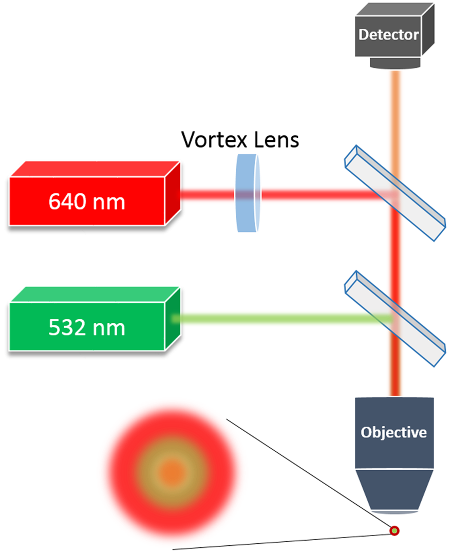
Figure 1: Schematic setup of STED microscope system showing the excitation (532 nm) and depletion (640 nm) lasers used to create the donut-shaped beam.
DOE are micro-optical window-like phase elements designed to modify the phase of the light that propagates through them to create various shaping functions, the main ones being multichannel splitting, spatial shaping, and focal shaping. In diffractive optics fabrication processes, similar methods to those used in the semiconductor industry are applied, giving DOE perfect angular accuracy with extremely low manufacturing tolerances. They are flat, thin, and easy to integrate into any opto-mechanical design. In many cases, DOE present a much more cost-effective beam shaping method than their refractive counterparts that frequently demand complex electro-opto-mechanics, making DOE a more robust solution when it comes to lifetime value.
The main production processes for DOE consist of several repeating steps including photoresist wafer coating followed by direct UV lithography and repeated etching directly into the fused silica substrate. This creates a binary pattern microstructure at the surface of the millimeter-scale thick optical window. To achieve optimal optical efficiency, up to 4 lithography steps are often applied to create 16 levels of microstructures. Figure 2 shows an actual diffractive structure of a 16-level vortex lens measured by an optical profilometer. The last step in the DOE manufacturing process is deploying an anti-reflective coating layer. DOE made of fused silica have an outstanding laser damage threshold, surface deviation and micro-roughness, and mechanical properties.
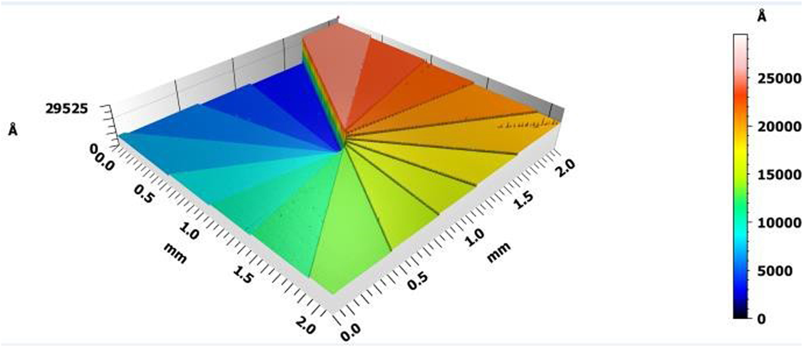
Figure 2: Diffractive surface of a 16-level VL DOE measured with an optical profilometer.
STED microscopy is a technique for measuring submicron structures, which requires the system to be highly precise and accurate. Otherwise, overall performance may be severely affected. The precision accuracy is where diffractive optics, with all the aforementioned advantages, fit in.
Optical system design tools are used worldwide to shorten development time, to decrease the number of prototyping iterations, and to reduce expenses all the way from prototype development to completion of the commercial product. Today's optical design solutions provide great tools for engineers to simulate and optimize optical system performance. One of these tools that is widely used in the photonics industry is Zemax OpticStudio®.
However, these tools are limited by what manufacturers are willing to share about the design and content of their components. Many engineers are strongly motivated to use standard off-the-shelf catalog parts as much as possible in their system design rather than using customized parts. In practice, however, seldom do catalog parts allow full simulation capabilities. Intellectual property protection, among other reasons, leads to catalog optical components and modules that cannot be simulated reliably and effectively, making it difficult for engineers to integrate and analyze their performance in their system design. This lack of analysis capabilities can result in unpleasant surprises when the purchased parts do not operate as expected or as defined in specifications.
Zemax introduced a partial solution to overcome this problem with their “Black Box models.” The Black Box allows users to perform a ray tracing analysis on a specific optical device while preventing them from seeing the internal structure of the device. Unfortunately, the Black Box models are limited to geometrical ray tracing and to Huygens point spread function (PSF) methods, and can be used only in sequential mode. In their article “How to design a confocal fluorescent microscope in OpticStudio” [Reference Brodsky and Kaplan1], Zemax used a custom-developed system in a non-sequential mode, but this option is not feasible when using catalog parts protected by Black Boxes.
In STED microscopy, the two key parts that are most challenging to model are the focusing objective and the vortex lens. Occasionally, a Black Box file for the focusing objective and a VL simulation for the physical optics [2] are available. However, it is unlikely that both will work in a sequential mode.
There are several known methods to model a VL in Zemax. The custom delay-locked loop (DLL) phase surface is one, grid phase sag is another, and stereolithography (STL) sag CAD files are the last (hybrid sequential or non-sequential mode). The most effective method for geometrical optics ray tracing is the custom DLL for phase surface developed by Holo/Or Ltd. With this method, aperture size is automatically adjusted and has variable parameters for topological charge “m” and sign to define the phase direction clockwise or counterclockwise.
Figure 3 summarizes the challenges of designing a STED optical system and the proposed solution for each.
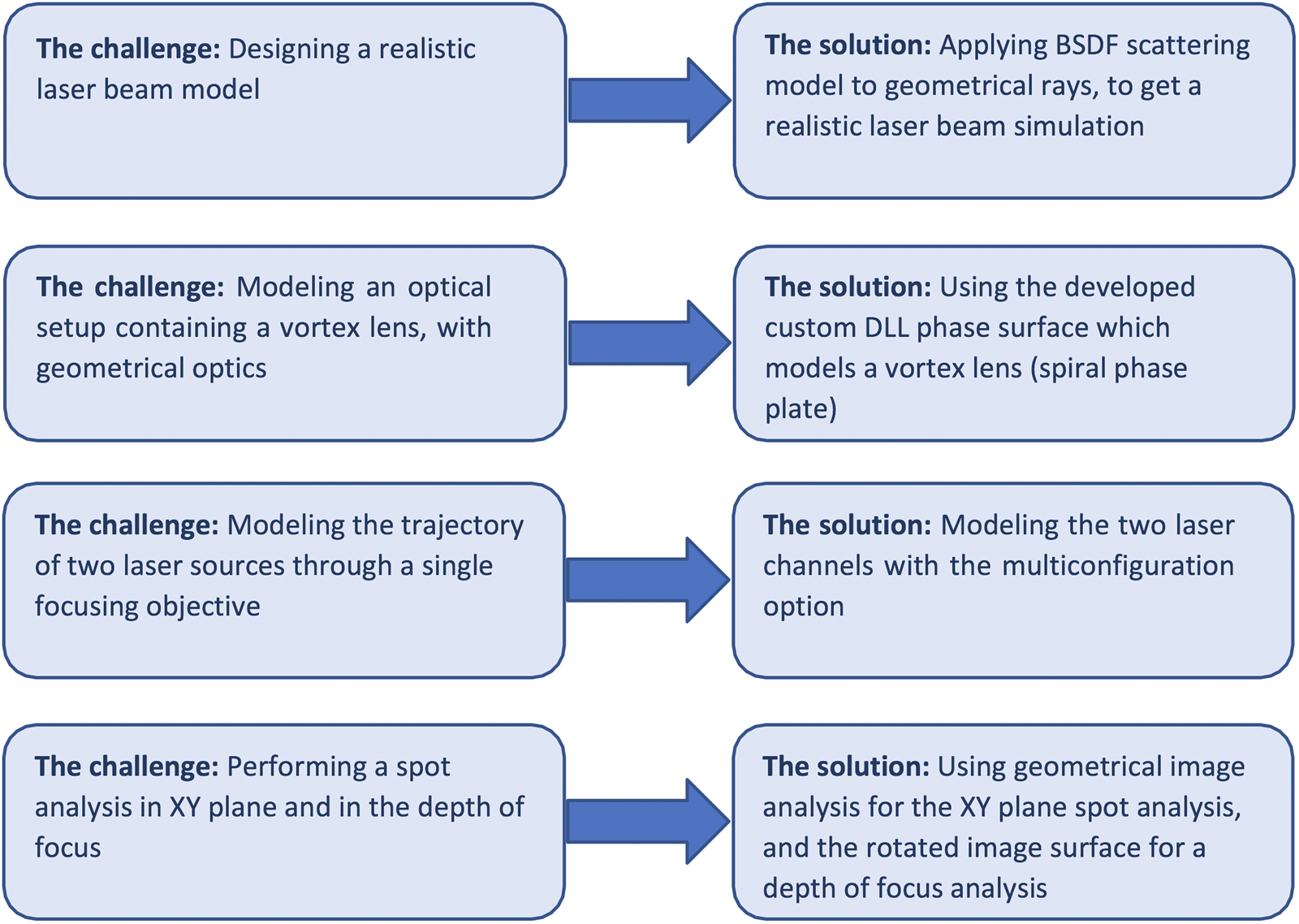
Figure 3: Design task challenges involved in the construction of a STED optical system and the proposed solution for each.
The simulation presented in this paper assumes a basic level of knowledge and understanding of lasers, optical elements, and their parameters. In addition, entry-level practice experience doing optical design with Zemax OpticStudio® or its alternatives is expected. The project begins with a general description of the optical setup (Figure 1): The system consists of two single-mode Gaussian lasers of different wavelengths, positioned on the same optical path. Both sources are focused by the same achromatic objective. The depletion laser effect is shaped by a SPP element (VL) into a donut-shaped spot. In this case, we chose a Thorlabs objective as an off-the-shelf catalog part, as it has a published Black Box available for download that we could use. Some of the other objective manufacturers and sellers offer to supply a Black Box upon request. The parameters used in the model are summarized in Table 1.
Table 1: Technical parameters of the modeled optical system:

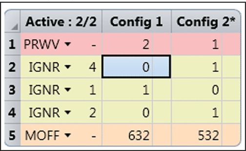
Table 2 contains a screenshot of the Zemax Lens Data Editor, in which each line represents an optical surface. An independent optical path for each laser is defined by the multiple configurations shown in Table 3.
Table 2: Zemax Lens Data Editor Layout of STED system.
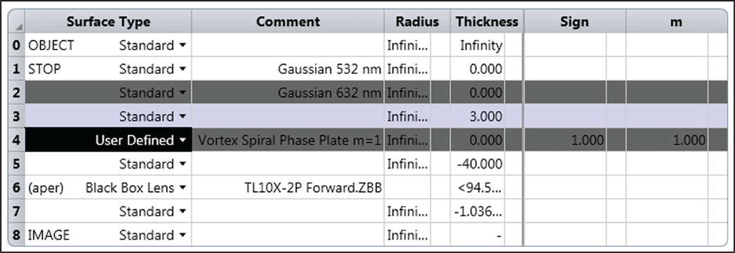
Table 3: Multiconfiguration Editor for Depletion and Excitation optical path.
Surface types 1 and 2 (Table 2) provide an optimized scattering effect to create a realistic spot size individually for each wavelength. In short, this method converts a geometrical point into a spot with physical dimensions, like a real light source [Reference Brodsky and Kaplan1]. The method is especially useful to simulate single-mode and multimode lasers within complex systems in both sequential and non-sequential modes, where other methods either completely fail or take a very long time to simulate. The correct scattering ratio should be defined according to the method described in [Reference Brodsky and Kaplan1] to achieve a realistic spot size.
Surfaces 3 and 4 (Table 2) refer to the VL element manufactured on a fused silica window. Surface 4 is a user-defined type of surface used to generate an ideal spiral phase. It is defined by sign for clockwise or counterclockwise azimuthal phase direction and topological charge “m” (number of accumulated 2-pi radians in 360o). The value of the topological charge for this surface does not have to be equal to the actual one and can be fractions of an integer (m-1.1, for example). The important thing is the physical correctness and consistency of the model. One must fine-tune the number around the real value and observe the resulting ring until a correct ratio of hole to ring that mirrors the SPP theoretical behavior is achieved.
The last element in the setup (Table 2, line 6) is the Black Box of the focusing objective. Line 8 is the image plane, which is positioned in the focal plane of the optical system.
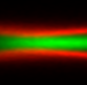
In Figure 4, the simulation results from the Geometrical Image Analysis (GIA) method window of the Zemax OpticStudio®, exported to Matlab for better visual presentation, are demonstrated. Figure 4a presents the spatial intensity distributions of the depletion, donut-shaped, optical channel; Figure 4b presents the excitation, Gaussian-distributed, optical channel; Figure 4c presents the difference between the depletion and excitation channels in super resolution; and Figure 4d presents the intensity profiles of the donut and Gaussian beams.
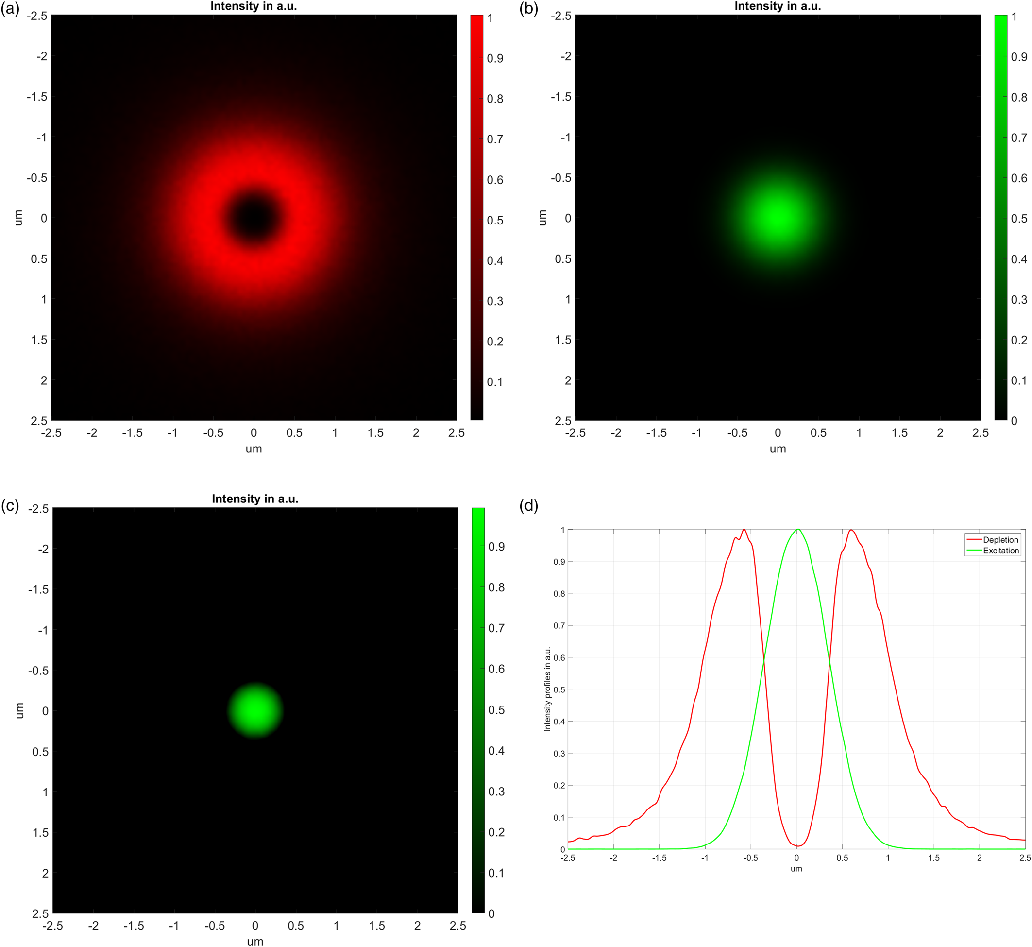
Figure 4: a, Spatial intensity distribution of the donut-shaped depletion laser; b, spatial intensity distribution of the Gaussian spot excitation laser; c, the difference between the depletion and the excitation channels; d, intensity profile of donut and Gaussian shapes.
Another interesting analysis that can be performed using the same Zemax model is a depth of focus (DOF) analysis. By simply rotating the image surface by 90o, the DOF behavior can be analyzed. This minor adjustment changes the plane presented by the GIA. Instead of presenting the standard XY plane, one can easily present either XZ or YZ planes and witness the light intensity behavior on the Z-axis. Such a simulation is useful to identify the waist position and to analyze the defocus range from a single image. Figures 5a–c demonstrate the DOF performance of each separate channel of the STED system and their combined performance on the XZ plane.
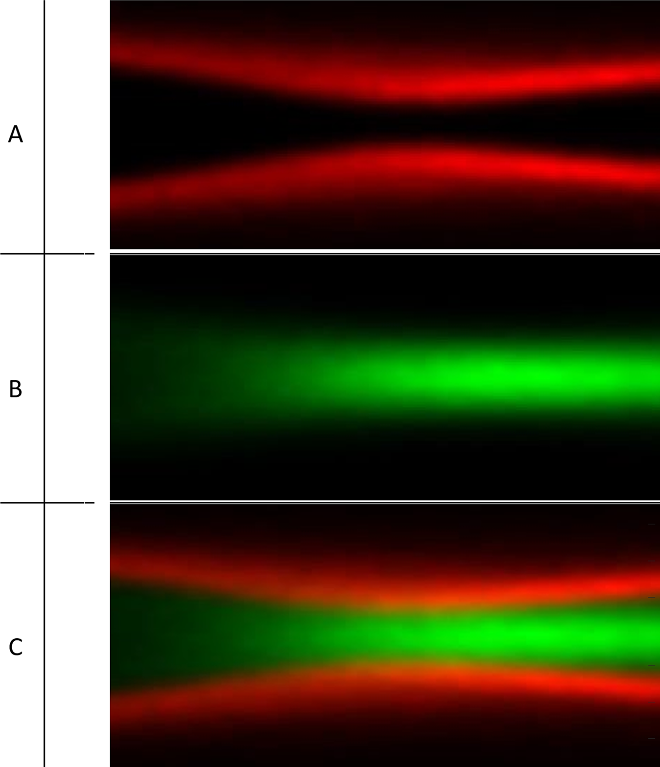
Figure 5: DOF simulation of the STED system - ZX intensity distribution in A.U. a, Depletion channel; b, excitation channel; c, combined view.
Conclusion
This article presents a method to model a simplified STED microscope using Zemax OpticStudio® design software. In the model we used real focusing objective specifications and the available objective Black Box. The scattering method, developed for simulating physical optical effects in raytracing, was used to obtain realistic performance of a diffractive vortex lens (spiral phase plate) and to generate a donut-shaped beam. In the model we demonstrated spatial intensity distribution on the XY plane and axial intensity distribution on the XZ plane. The proposed concept allows modeling and analysis of complex optical microscopy systems, including multiple channels, scanning, and detection, with short simulation times as in geometrical ray tracing and performance close to physical optics in terms of modeling accuracy.


