


I. INTRODUCTION
Slow-wave transmission lines are artificial lines exhibiting small phase velocity as compared with ordinary lines [Reference Wu and Webster1, Reference Martín2]. This slow-wave effect is typically achieved by externally loading a host line with reactive elements, including distributed [Reference Chuang3–Reference Koziel and Kurgan10] or lumped/semi-lumped (i.e. electrically small) components [Reference Hirota, Minakawa and Muraguchi11–Reference Morimoto, Waghmare, Dhwaj and Itoh34]. Most realizations of slow-wave transmission lines based on lumped or semi-lumped components use periodic capacitive loading [Reference Hirota, Minakawa and Muraguchi11–Reference Coromina, Selga, Vélez, Bonache and Martín24]. By periodically loading the host line with shunt capacitors, the effective capacitance of the line is enhanced, and therefore the phase velocity is reduced. Alternatively, series connected inductances have been used as a means to achieve the slow-wave effect (in this case resulting as consequence of the enhancement of the effective line inductance) [Reference Zhu26–Reference Selga, Vélez, Bonache and Martín29]. Obviously, by replacing the ordinary lines with slow-wave artificial lines exhibiting the required characteristic impedance and electrical length at the design frequency, it is possible to substantially reduce the size of the microwave components. Additionally, if the slow-wave transmission lines are periodic, it is possible to suppress undesired spurious or harmonic bands by virtue of the Bragg effect, related to periodicity and providing stop bands in the transmission response of the artificial lines [Reference Martín2, Reference Yablonovitch35, Reference Joannopoulos, Meade and Winn36].
The implementation of slow-wave transmission lines with simultaneous inductive and capacitive loading is less common [Reference Liu, Fang, Wang and Zhou32, Reference Selga, Vélez, Bonache and Martín37, Reference Selga, Vélez, Coromina, Fernández-Prieto, Bonache and Martín38]. The presence of both reactive elements is useful in order to achieve further levels of miniaturization. Moreover, further design flexibility can be achieved due to the presence of both reactive elements. In this paper, we report a slow-wave transmission line implemented in coplanar waveguide (CPW) technology by loading the line with capacitive and inductive elements. The shunt capacitors are implemented by means of transverse strips, etched in the back substrate side of the CPW, similar to the work presented in [Reference Seki and Hasegawa39]. The series inductive elements are implemented by etching rectangular slots in the ground plane, following the approach first presented in [Reference Vélez, Selga, Bonache and Martín28] by some of the authors. Then these lines are applied to the miniaturization and harmonic suppression of a power splitter based on a slow-wave impedance inverter.
The work is organized as follows. In Section II, the circuit schematic and the topology of these lines are reported, and the expressions providing the electrical length of the unit cell and the characteristic impedance are derived from Floquet analysis of periodic structures. The number of cells necessary to efficiently suppress the harmonic responses in quarter-wavelength impedance inverters (later used for the implementation of a power splitter) is also obtained in this section. Section III is focused on the synthesis of a 35.35 Ω slow-wave impedance inverter. The designed and fabricated power splitter is reported in Section IV. Finally, the main conclusions are highlighted in Section V.
II. SLOW-WAVE TRANSMISSION LINE: TOPOLOGY, CIRCUIT SCHEMATIC, AND ANALYSIS
The topology (unit cell) and circuit schematic of the proposed slow-wave CPW transmission lines are depicted in Fig. 1. The host line is described by the characteristic impedance Z 0, and by the electrical length (kl), where k is the phase constant and l is the total (physical) length of the unit cell. The loading reactive elements are the series inductance, L ls, and the shunt capacitance, C ls. Losses are excluded in this model.
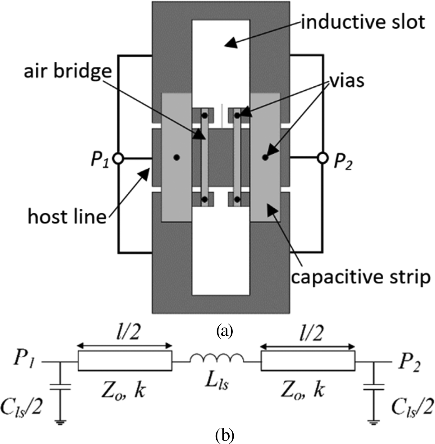
Fig. 1. Topology (unit cell) (a) and circuit schematic (b) of the slow-wave CPW transmission line under consideration.
The unit-cell electrical length, βl, and characteristic impedance, Z B, of the loaded line are given by [Reference Martín2, Reference Pozar40]:
 $$\cos (\beta l) = A$$
and
 $$Z_B = \displaystyle{B \over {\sqrt {A^2 - 1}}}, $$
where A and B are the first row elements of the transmission ABCD matrix of the two-port unit cell (note that expressions (1) and (2) are valid as long as the structure is symmetric with regard to the midplane between the input and the output ports).
The circuit schematic of Fig. 1(b) is composed by the cascade of five simple two-ports, consisting of shunt capacitors (external two-ports), series inductor (central two-port), and transmission line sections (intermediate two-ports). The ABCD matrix of the whole structure is given by the product of the individual matrices of each constitutive two-port, given by:
 $$[{\bf A}]_L = \left( {\matrix{ 1 & {L\omega j} \cr 0 & 1 \cr}} \right)$$
 $$[{\bf A}]_C = \left( {\matrix{ 1 & 0 \cr {C\omega j} & 1 \cr}} \right)$$
 $$[{\bf A}]_{TL} = \left( {\matrix{ {\cos (kl)} & {jZ_0\sin (kl)} \cr {\displaystyle{j \over {Z_0}}\sin (kl)} & {\cos (kl)} \cr}} \right),$$
where the subscripts L, C, and TL are used to differentiate the ABCD matrices of a series inductance, L, shunt capacitance, C, and transmission line section with electrical length kl and characteristic impedance Z 0, respectively. From expressions (3), the ABCD matrix of the two-port of Fig. 1(b) can be easily inferred, and expressions (1) and (2) are found to be:
 $$\eqalign{\cos (\beta l) & = \cos (kl) - \left( {\displaystyle{{L_{ls}} \over {2Z_0}} + \displaystyle{{C_{ls}Z_0} \over 2}} \right)\omega \sin (kl) \cr & \quad - \displaystyle{{L_{ls}C_{ls}} \over 2}\omega ^2\cos ^2(kl/2),} $$
 $$Z_B = \displaystyle{{ - jB} \over {\sin (\beta l)}} \equiv \displaystyle{{Z_0\sin (kl) + \omega L_{ls}\;{\cos} ^2(kl/2)} \over {\sin (\beta l)}},$$
where ω is the angular frequency. The unit-cell electrical length, βl, and characteristic impedance, Z B, of the loaded lines are design parameters, given by the specific application. An additional bound for the four unknowns (Z 0, kl, L ls, and C ls) is given by the so-called slow-wave ratio, swr, defined by
 $$swr = \displaystyle{{v_{pL}} \over {v_{po}}} = \displaystyle{{\omega /\beta} \over {\omega /k}} = \displaystyle{{kl} \over {\beta l}},$$
where v pl and v po are the phase velocities of the loaded and unloaded lines, respectively. The swr is a fundamental parameter determining the miniaturization level. Theoretically, the physical length of the slow-wave transmission line, as compared with one of the ordinary lines, is dictated by the swr. However, the reactive elements loading the line have finite size and, hence, the length reduction given by the swr is not achievable in practice.
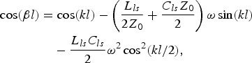
Note that once βl and swr are set to a certain value (the former given by design specifications and the latter dictated by the compactness level required), kl is given by (6). However, the three remaining parameters characterizing the unit cell of Fig. 1(b), i.e. Z 0, L ls, and C ls, are not univocally determined by equations (4) and (5). As Z 0 increases, C ls increases and L ls decreases (see Fig. 2). Hence, a tradeoff is necessary in order to avoid extreme values of L ls and C ls.
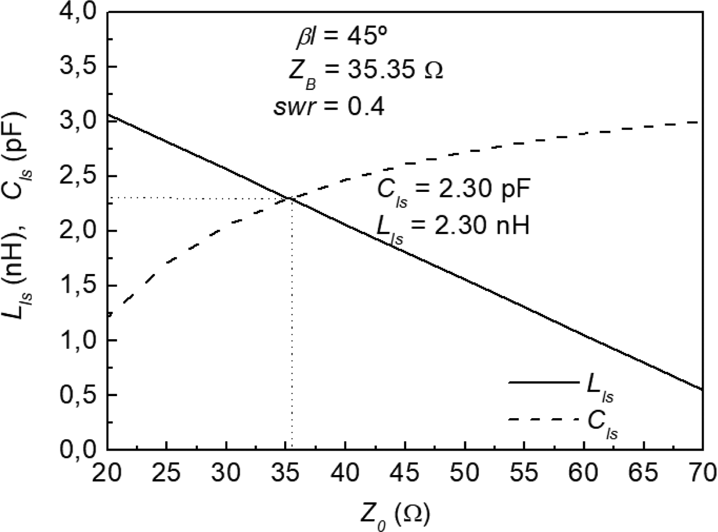
Fig. 2. Variation of L ls and C ls with Z 0 that result from the solution of (4)–(6) with βl = 45°, Z B = 35.35 Ω, and swr = 0.4.
Another important parameter is the number of cells of each transmission line section under consideration, N. This parameter determines the bandwidth and position of the stop band of the periodic structure, and is therefore relevant in applications where spurious or harmonic suppression is desired. Of particular interest is the cutoff frequency of the slow-wave transmission line, which corresponds to the onset of the stop band. This frequency can be determined from (4). Let us consider that the required electrical length of the slow-wave transmission line is θ, and that such line is implemented with N unit cells (i.e. βl = θ/N). In the limit of the first transmission band, βl = π (just above this frequency β is purely imaginary). Therefore, the cutoff frequency, f C, can be inferred from the first frequency satisfying:
 $$\eqalign{- 1 & = \cos \left( {swr\displaystyle{\theta \over N}\displaystyle{\omega \over {\omega _0}}} \right) - \left( {\displaystyle{{L_{ls}} \over {2Z_0}} + \displaystyle{{C_{ls}Z_0} \over 2}} \right)\omega \sin \left( {swr\displaystyle{\theta \over N}\displaystyle{\omega \over {\omega _0}}} \right) \cr & \quad - \displaystyle{{L_{ls}C_{ls}} \over 2}\omega ^2\cos ^2\left( {swr\displaystyle{\theta \over {2N}}\displaystyle{\omega \over {\omega _0}}} \right)}$$
and note that this frequency depends on N, as anticipated. Inspection of (7) reveals that this equation has multiple solutions. In particular, the frequencies satisfying
 $$swr\displaystyle{\theta \over N}\displaystyle{\omega \over {\omega _0}} = (2n + 1)\pi {\rm, with}\; n = 0,1,2,...$$
correspond to the upper limits of the multiple stop bands that these periodic structures support. The solution that results by considering n = 0 provides the upper limit of the first stop band, the one of interest, i.e.
 $$\omega _s = 2\pi f_s = \displaystyle{{N\omega _0\pi} \over {swr \cdot \theta}}. $$
For which concern the lower limit of that band, f C, it is not possible to obtain it analytically from (7). Despite the fact that such frequency can be solved numerically, it can be estimated from the approximate lumped element model of the structure, given in Fig. 3, namely [Reference Martín2]
 $$f_C = \displaystyle{1 \over {\pi \sqrt {(L + L_{ls})(C + C_{ls})}}}. $$
Fig. 3. Lumped element equivalent circuit of the unit cell of Fig. 1.
Note that the validity of this approximation improves as the loading reactive elements increase as compared with the element values describing the host line (L and C), as discussed in [Reference Martín2]. Since large element values are necessary to achieve small slow-wave ratios, swr, it follows that the estimation of f C from the lumped element model is reasonable in applications where high compactness levels are pursued.
According to the lumped element circuit model, the electrical length of the unit cell can be expressed as
 $$\beta l = \displaystyle{\theta \over N} = 2\pi f_0\sqrt {(L + L_{ls})(C + C_{ls})}. $$
Consequently, the cutoff frequency and the design frequency are related by
 $$\displaystyle{{f_C} \over {f_0}} = \displaystyle{{2N} \over \theta}. $$
Expression (12) is fundamental in order to determine the number of cells, N, necessary to efficiently suppress spurious or harmonic bands. For quarter-wavelength impedance inverters, with θ = π/2, and devices based on it, the first harmonic band appears at 3f 0. This means that (12) must be smaller than 3 if the first harmonic band must be suppressed, and, as a result, N = 1 or 2. In principle, the preferred solution should be N = 2 for two main reasons: (i) f C is more separated from f 0, avoiding the alteration of the response in the region of interest, and (ii) the stop band bandwidth is larger since, according to (9), f s is also larger with N = 2. Nevertheless, the frequency given by (9) with N = 2 is typically very large, and the predictions of the model of Fig. 1 in the vicinity of that frequency do not match with the responses of any planar implementation of the structure, since the lumped elements L ls and C ls do not provide a good description of the semi-lumped (electrically small and planar) components that are typically used (transverse strips for the capacitors and slots in the ground planes for the inductors, in the present work, based on slow-wave CPWs). Thus, in any practical scenario, the upper frequency of the stop band inferred from (9) is overestimated. Despite of that fact, the harmonic suppression efficiency improves by choosing N = 2. Since the device proposed in this paper, a compact and harmonic suppressed power splitter, is based on an impedance inverter, the number of cells of the constitutive slow-wave transmission line (acting as impedance inverter) is N = 2.
III. SYNTHESIS OF THE SLOW-WAVE IMPEDANCE INVERTER
The slow-wave impedance inverter under consideration, to be later applied to the design of a compact power splitter, has an impedance of Z B = 35.35 Ω, and, obviously, an electrical length of θ = 90° (the considered operating frequency has been set to f 0 = 1 GHz). According to the previous section, the number of cells of the inverter is set to N = 2; consequently, βl = 45°. We have set the slow-wave ratio to swr = 0.4, and, therefore, kl = 18°. Note that the remaining unknowns, Z 0, C ls, and L ls, are not unequivocally determined from (4) and (5). We have set the characteristic impedance of the host line to Z 0 = 35.35 Ω, providing the following reactive values: C ls = 2.30 pF and L ls = 2.30 nH, which are easily implementable in CPW technology. Nevertheless, the variation of C ls and L ls with Z 0 is depicted in Fig. 2, from which it follows that by choosing Z 0 = 35.35 Ω, extreme reactive values are avoided.
Once the element values of the circuit of Fig. 1(b) are determined, the next step is the generation of the layout. As mentioned in the introduction, our aim in the paper has been the implementation of the inverter (and the subsequent power splitter) in CPW technology by loading the line with inductive slots in the ground plane and capacitive transverse strips in the back substrate side (the latter connected to the central strip of the CPW by means of vias). To this end, we have independently determined the slot dimensions providing the required inductance values, as well as the dimensions of the transverse strips necessary to achieve the necessary shunt capacitance. Nevertheless, some post-optimization has been necessary to adjust the characteristic impedance and electrical length to the design values at the operating frequency. The layout of the unit cell, as well as the characteristic impedance and electrical length are depicted in Fig. 4. It can be appreciated that the required characteristic impedance (Z B = 35.35 Ω) at f 0 is achieved and the electrical length of the unit cell is roughly the nominal value of 45° (thus providing an electrical length of 90° for the two-cell, i.e. N = 2, impedance inverter). The considered substrate is Rogers RO3010 with thickness h = 1.27 mm, dielectric constant ε r = 10.2, and loss tangent tanδ = 0.0023.
Fig. 4. Layout (a), characteristic impedance (b), and electrical length (c) of the inverter unit cell. Dimensions are: L w = 3.20 mm, W w = 4.9 mm, L C = 1.7 mm, W C = 7.14 mm, w = 3.2 mm, s = 0.32 mm.
IV. DESIGNED AND FABRICATED SLOW WAVE SPLITTER
The layout of the designed slow-wave power splitter is depicted in Fig. 5, where it is compared to the layout of the conventional CPW implementation. The simulated frequency response of both structures, inferred from Keysight Momentum, can be seen in Fig. 6. It can be appreciated that the response of the slow-wave power splitter is roughly the same than one of the ordinary splitters in the region of interest (vicinity of f 0). However, the first (at 3f 0) and second (at 5f 0) harmonic bands of the conventional splitter are significantly suppressed in the slow-wave implementation.
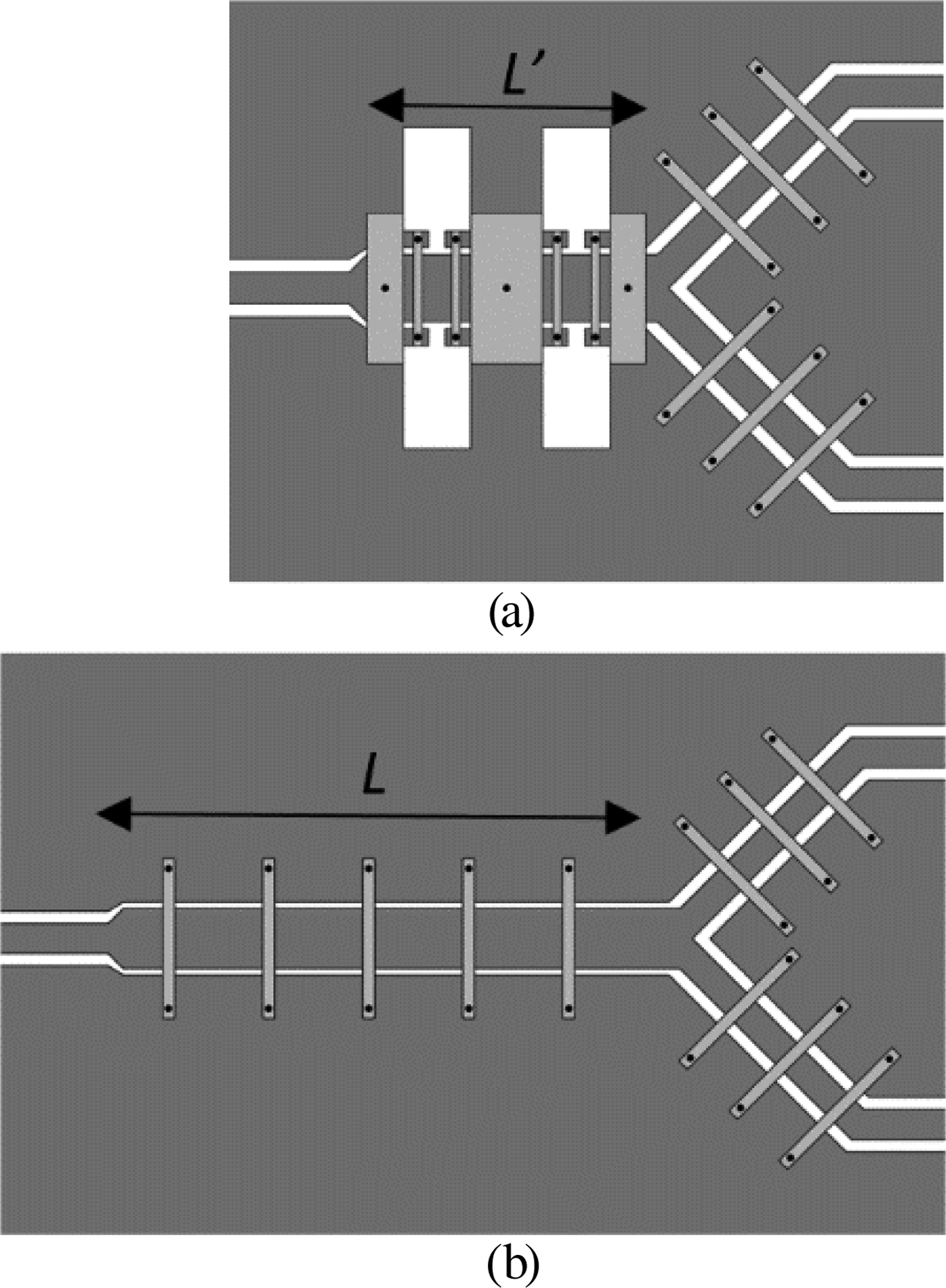
Fig. 5. Layouts of the slow-wave (a) and ordinary (b) CPW power splitters. These layouts are drawn to scale for easy comparison. Relevant dimensions (i.e. inverter lengths) are: L′ = 13.20 mm and L = 27.27 mm.
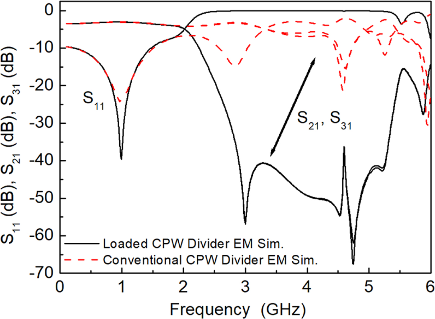
Fig. 6. Simulated frequency response of the splitters of Fig. 5.
The designed slow-wave power splitter has been fabricated by means of a LPKF-H100 drilling machine. The photograph is depicted in Fig. 7, whereas the measured response, inferred by means of the Keysight PNA 5221A vector network analyzer, is shown in Fig. 8, where it is compared to the simulated response. The agreement between both responses is very good. The measured matching at f 0 is S 11 = −35 dB, whereas the measured power splitting is S 21 = −3.3 dB and S 31 = −3.2 dB. These values are good, with power splitting very close to the ideal value of −3 dB. Concerning the filtering capability of the designed slow-wave splitter, the measured rejection levels at the harmonic frequencies are better than 49 dB (at 3f 0) and 23 dB (at 5f 0).
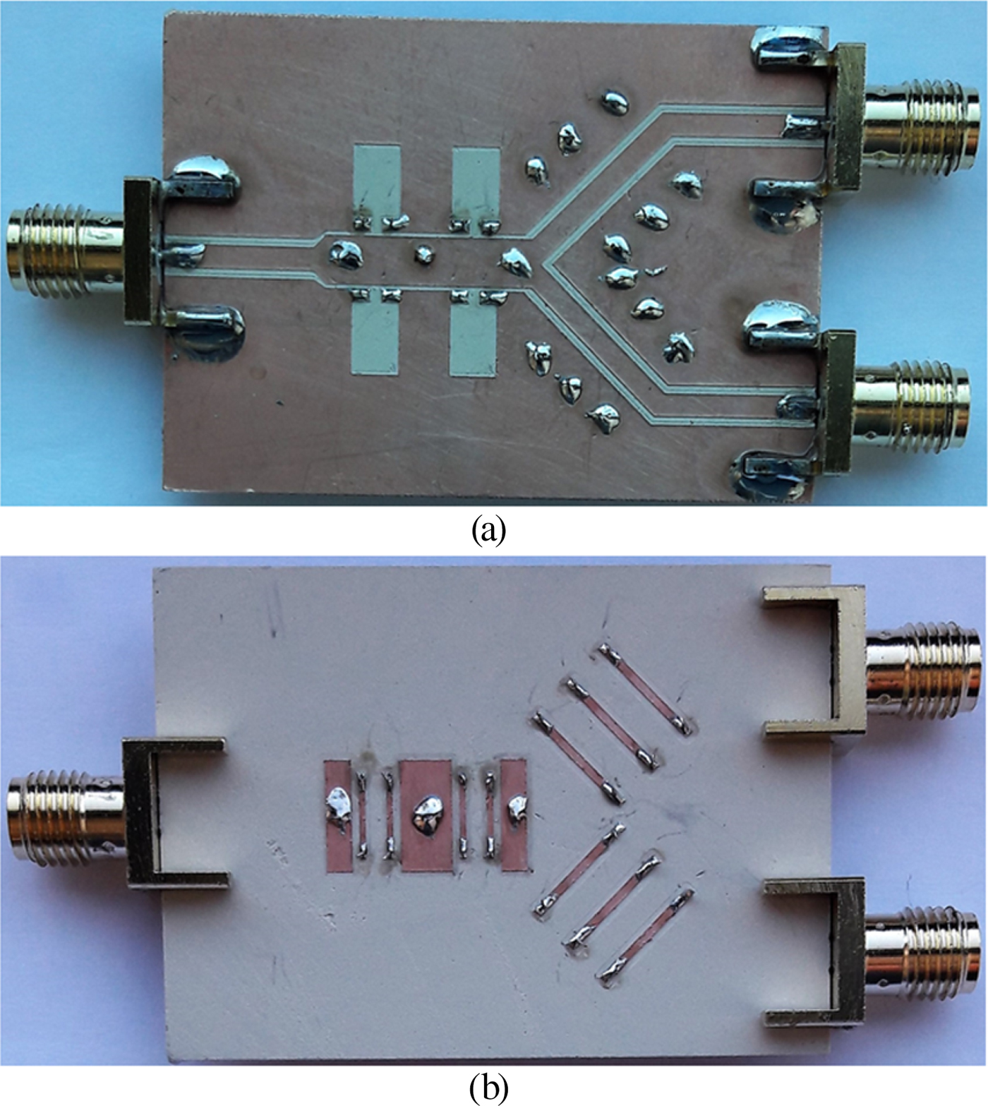
Fig. 7. Photograph of the fabricated slow-wave power splitter. (a) Top; (b) bottom.
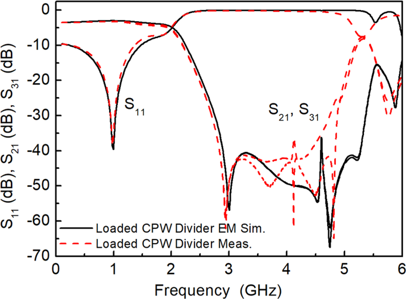
Fig. 8. Measured and simulated frequency response of the designed and fabricated slow-wave splitter.
Concerning dimensions, it is remarkable that the length of the slow-wave inverter used to implement the splitter is 48% the length of the ordinary counterpart. Obviously the form factor in the proposed slow-wave inverter is worst as compared with one of the conventional inverters, i.e. the new inverter is wider, due to the inductive slots etched in the ground plane. Nevertheless, the key parameter for the splitter in terms of size is the inverter length, since the transverse dimensions of the whole splitter are dictated by the output access lines.
Compact power splitters implemented by means of left-handed or composite right- and left-handed lines with similar size reduction to the one achieved in this paper have been reported [Reference Gil, Bonache, Gil, García-García and Martín41, Reference Sisó, Bonache and Martín42]. In [Reference Gil, Bonache, Gil, García-García and Martín41], the bandwidth of the reported splitter is smaller than one of the conventional counterparts, contrary to the splitter reported in this paper, where bandwidth is very similar to one of the conventional splitters, as Fig. 8 indicates. Moreover, the splitter in [Reference Gil, Bonache, Gil, García-García and Martín41] does not have harmonic suppression capability. With regard to the splitter of [Reference Sisó, Bonache and Martín42], size reduction of the constitutive lines is comparable. However, the device in [Reference Sisó, Bonache and Martín42] is focused on dual-band functionality, and for this reason, comparing device performance is not significant in this case.
V. CONCLUSION
In conclusion, a CPW slow-wave power splitter with reduced size and harmonic suppression capability has been presented in this paper. Size reduction and harmonic suppression has been achieved by implementing the 35.35 Ω quarter-wavelength impedance inverter, necessary to achieve the power division by the considered topology, by means of a capacitively and inductively loaded slow-wave CPW transmission line. The series inductors have been implemented by means of rectangular slots, etched in the ground plane, whereas the shunt capacitive effect has been achieved by etching transverse strips in the back substrate side, connected to the central strip of the CPW line through metallic vias. The device has been fabricated, and the measured response has shown that the device functionality at the design frequency has been achieved, with very similar response to one of the ordinary CPW implementation in the region of interest. However, because the Bragg effect is associated with periodicity, a band gap in the inverter response opens, and this has been used to reject the first harmonic bands of the designed power splitter. The proposed structure is a multifunctional device with power splitting and filtering capability simultaneously, of interest in applications where size is a critical aspect.
ACKNOWLEDGEMENT
This work was supported by MINECO-Spain (projects TEC2013-40600-R, TEC2016-75650-R, TEC2013-41913-P), Generalitat de Catalunya (project 2014SGR-157), Institució Catalana de Recerca i Estudis Avançats (who awarded Ferran Martín), the Spanish Junta de Andalucía (project P12-TIC-1435), and FEDER funds.
 Francisco Aznar-Ballesta was born in Granada, Spain, in 1978. He received the Electronics Engineering degree from the Universidad de Granada (UGR) in 2005 and the Ph.D. degree in Electronics Engineering from the Universitat Autònoma de Barcelona (UAB) in 2009. After a postdoctoral stay in the Universidad Carlos III de Madrid (UC3M), he joined in 2012 the Universidad Politécnica de Madrid (UPM), where he is currently a Professor. In 2013, he worked in the Institüt für Mikrowellentechnik und Photonik in the Tecknische Universität Darmstadt (TUD), within the José Castillejo MINECO Program. He is currently collaborator researcher in CIMITEC (Departament d'Enginyeria Electrònica) at UAB. His current research interests include design, miniaturization, and characterization of passive RF/microwave circuits and metamaterials-based sensors.
 Jordi Selga was born in Barcelona, Spain, in 1982. He received the B.S. degree in Telecommunications Engineering – Electronic Systems in 2006, the M.S. degree in Electronics Engineering in 2008 and the Ph.D. degree in Electronics Engineering in 2013 from the Universitat Autònoma de Barcelona (UAB), Barcelona, Spain. Since 2008, he is a member of CIMITEC-UAB, a research center on Metamaterials supported by TECNIO (Catalan Government). He was a holder of a national research fellowship from the Formación de Profesorado Universitario Program of the Education and Science Ministry (Reference AP2008-4707). He is currently working in subjects related to metamaterials, CAD design of microwave devices, EM optimization methods, and automated synthesis of planar microwave components at the UAB.
 Paris Vélez was born in Barcelona, Spain, in 1982. He received the degree in Telecommunications Engineering, specializing in electronics, the Electronics Engineering degree, and the Ph.D. degree in Electrical Engineering from the Universitat Autònoma de Barcelona, Barcelona, in 2008, 2010, and 2014, respectively. His Ph.D. thesis concerned common mode suppression differential microwave circuits based on metamaterial concepts and semi-lumped resonators. During the Ph.D., he was awarded with a pre-doctoral teaching and research fellowship by the Spanish Government from 2011 to 2014. He is currently involved in the subjects related to metamaterials sensors for fluidics detection and characterization at LAAS-CNRS through a TECNIOSpring fellowship cofounded by the Marie Curie program. His current research interests include the miniaturization of passive circuits RF/microwave and sensors-based metamaterials. Dr. Vélez is a Reviewer for the IEEE Transactions on Microwave Theory and Techniques and for other journals.
 Armando Fernández-Prieto was born in Ceuta, Spain, in September 1981. He received the Licenciado and Ph.D. degrees in Physics from the University of Seville, Seville, Spain, in 2007 and 2013, respectively. He is currently involved with post-doctoral research with the Microwaves Group, University of Seville. His research interests focus on printed passive microwave components and metamaterials. Dr. Fernández-Prieto is a reviewer for the IEEE Transactions on Microwave Theory and Techniques, as well as for many other journals.
 Jan Coromina was born in Barcelona, Spain, in 1989. He received the B.S. degree in Electronics Engineering for Telecommunication in 2014 and the Master's degree in Telecommunications Engineering in 2017 from the Universitat Autònoma de Barcelona (UAB), Barcelona, Spain. He is currently carrying out his Ph.D. degree within the research center CIMITEC (Departament d'Enginyeria Electrònica) at UAB, on the field of microwave circuit design and miniaturization. In 2016, he joined the company IDNEO Technologies as an RF engineer, where he developed ISM antennas for industrial applications, and multi service LNA for the automotive sector.
 Jordi Bonache was born in 1976 in Barcelona (Spain). He received the Physics and Electronics Engineering degrees from the Universitat Autònoma de Barcelona in 1999 and 2001, respectively, and the Ph.D. degree in Electronics Engineering from the same university in 2007. In 2000, he joined the “High Energy Physics Institute” of Barcelona (IFAE), where he was involved in the design and implementation of the control and monitoring system of the MAGIC telescope. In 2001, he joined the Department of Electronics Engineering of the Universitat Autònoma de Barcelona where he is currently an Associate Professor. From 2006 to 2009, he worked as an executive manager of CIMITEC. Currently he is leading the research in RFID and antennas in CIMITEC. His research interests include active and passive microwave devices, metamaterials, antennas, and RFID.
 Ferran Martín was born in Barakaldo (Vizcaya), Spain in 1965. He received the B.S. degree in Physics from the Universitat Autònoma de Barcelona (UAB) in 1988 and the Ph.D. degree in 1992. From 1994 up to 2006, he was an Associate Professor in Electronics at the Departament d'Enginyeria Electrònica (Universitat Autònoma de Barcelona), and since 2007 he is a Full Professor of electronics. In recent years, he has been involved in different research activities including modeling and simulation of electron devices for high-frequency applications, millimeter wave and THz generation systems, and the application of electromagnetic bandgaps to microwave and millimeter wave circuits. He is now very active in the field of metamaterials and their application to the miniaturization and optimization of microwave circuits and antennas. He is the head of the Microwave Engineering, Metamaterials and Antennas Group (GEMMA Group) at UAB, and director of CIMITEC, a research center on metamaterials supported by TECNIO (Generalitat de Catalunya). He has organized several international events related to metamaterials, including Workshops at the IEEE International Microwave Symposium (years 2005 and 2007) and European Microwave Conference (2009), and the Fifth International Congress on Advanced Electromagnetic Materials in Microwaves and Optics (Metamaterials 2011), where he has acted as chair of the Local Organizing Committee. He has acted as Guest Editor for three special issues on metamaterials in three international journals. He has authored and co-authored over 500 technical conference, letter, journal papers, and book chapters; he is a co-author of the book on metamaterials entitled Metamaterials with Negative Parameters: Theory, Design and Microwave Applications (John Wiley & Sons Inc. 2008), author of the book Artificial Transmission Lines for RF and Microwave Applications (John Wiley & Sons Inc. 2015), and he has generated 17 Ph.D.s. Ferran Martín has filed several patents on metamaterials and has headed several development contracts. Prof. Martín is a member of the IEEE Microwave Theory and Techniques Society (IEEE MTT-S). He is a reviewer of the IEEE Transactions on Microwave Theory and Techniques and IEEE Microwave and Wireless Components Letters, among many other journals, and he serves as a member of the Editorial Board of IET Microwaves, Antennas and Propagation and International Journal of RF and Microwave Computer-Aided Engineering. He is also a member of the Technical Committees of the European Microwave Conference (EuMC) and International Congress on Advanced Electromagnetic Materials in Microwaves and Optics (Metamaterials). Among his distinctions, Ferran Martín has received the 2006 Duran Farell Prize for Technological Research, he holds the Parc de Recerca UAB – Santander Technology Transfer Chair, and he has been the recipient of two ICREA ACADEMIA Awards (calls 2008 and 2013). He is a Fellow of the IEEE since 2012 and Fellow of the IET since 2016.


