


Introduction
Multiple techniques are currently available for observing particles at the nanoscale. Scanning electron microscopy (SEM), atomic force microscopy (AFM), and energy dispersive X-ray spectroscopy (EDS) are some that are commonly employed in industry and academic laboratories. Nevertheless, even if each technique is very efficient in obtaining one particular type of information, extracting further information may require a correlative combination of these. In France, regulatory authorities require producers and suppliers of products involving nanoparticles to clearly determine the size and size distribution of each nanoparticle population [1]. This step remains a challenge in the case of nanoparticle mixtures.
In most cases, it is possible to discriminate particles in a mixture with only SEM because particles are different in size and/or shape (Figure 1, left). Unfortunately, it is also possible to be confronted with a mixture where particles are chemically different but very similar in size and shape as shown on the right in Figure 1.

Figure 1: SEM image of a mixture of SiO2 and TiO2 nanoparticles (left) and ZnO and TiO2 nanoparticles (right) contained in a drug (skin cream).
In this particular case, the correlation of AFM/SEM/EDS measurements provides a solution for discriminating the two populations. The SEM has a resolution of around 1 nm in the XY plane, but a single micrograph produces no quantitative information in the Z direction. AFM tip shape convolution results in reduced lateral resolution (x,y) of nano-objects, while measurements along the vertical axis (Z) are well-resolved. EDS mapping can be used to collect additional information to chemically classify the particles. But correlation of data collected by the three techniques is only possible if the data provided by the different instruments can be loaded, processed, and correlated with one unique software program.
Materials and Methods
Materials.
In this paper, which presents a feasibility study, Fe2O3 and ZnO nanoparticles were selected for their easily recognizable shapes and for their well-separated X-ray peaks (Zn L α, 1.012 keV; Fe L α, 0.705 keV) that can be easily detected at a very low voltage (typically 3 keV) with an appropriate EDS detector, thus protecting the sample from contamination and charging effects.
Two suspensions of Fe2O3 and ZnO powders commonly used in cosmetics were prepared by dispersion in ultra-pure water. In most cases, this kind of preparation (powder directly in water) leads to agglomeration/aggregation of the particles in the solution. To avoid agglomeration and correctly disperse the particles in the solution, an ultrasonic gun and bath were used. The sonicator generates vibrations amplified and transmitted to the solution by the probe, producing micrometric bubbles. These bubbles are subject to great external pressure, which results in bursting. The dissipate energy breaks the weak bonds in the agglomerates in the suspension.
To perform measurements on the same object using different equipment, a specific substrate must be used to facilitate localization. The system used is described in [Reference Crouzier2]. It consists of a silicon chip on which crosses and labels are lithographed. The substrate is robust, can be easily handled, and has low roughness, which is ideal for observation of nanoparticles by AFM. Moreover, it is conductive enough to avoid the low-voltage charging effects familiar to SEM and EDS users.
Deposition of nanoparticles.
The deposition step must also avoid agglomeration as much as possible. First, the particles must adhere when they are in contact with the substrate. Indeed, if the particles have an electrical charge of the same sign as the substrate, the repulsive electrostatic forces prevent the particles from adhering. Thus, either the particle charge or the substrate charge must be controlled. Here, the substrate charge was modified. Several solutions exist and could be used for this, such as adding polymer chains to the substrate [Reference Eklöf3–Reference Boyd and Cuenat5], but at the Laboratoire National de Métrologie et D'essais (LNE) a glow discharge treatment with a specific gas atmosphere (ELMO™, Cordouan Technologies) is used [Reference Ravelli6,Reference Dubochet7]. Depending on the gas used, this system can make the substrate hydrophilic or hydrophobic and positively or negatively charged. In our study, an electrical discharge was produced in an amylamine atmosphere to obtain a hydrophobic positively charged substrate.
As the particles tend to agglomerate during static deposition [Reference Thill and Spalla8,Reference Kralchevsky and Nagayama9] leading to the well-known “coffee-ring effect” [Reference Lohani10], a strategy must be deployed to avoid this phenomenon. Thus, a spin-coating deposition method was used [Reference Delvallée11]. With this technique, the droplet is spread out on the entire chip surface to achieve a homogeneous deposit of the particles at a surface concentration similar to that found in the suspension. The deposit is performed in two steps:
• First, a droplet (7.5 μL) is spread on the substrate at low rotation speed (between 300 rpm and 1200 rpm). During this step, the particles undergo a Brownian-type movement. The random motion of the suspended particles is such that a proportion of particles is deposited on the substrate.
• Then, the substrate is submitted to a very high rotation speed (8000 rpm). During this step, the solvent and particles that have not interacted with the substrate are ejected from the substrate.
To summarize the different stages of the deposition:
• Substrates are pre-treated in the ELMO™ effluent system with an amylamine atmosphere to positively charge them and to make them hydrophobic.
• A droplet of the Fe2O3 suspension is deposited on the substrate by spin coating.
• The substrate with the deposited Fe2O3 particles is treated again with the ELMO™ system with the same parameters.
• A droplet of the ZnO suspension is deposited on the substrate which had the Fe2O3 particles deposited by spin-coating.
The final deposit is shown in Figure 2.

Figure 2: SEM image of deposited Fe2O3 and ZnO mixture.
Instrumentation
Atomic force microscopy.
A Veeco Nanoman V equipped with a three-axis scanner operating under closed loop control (hybrid XYZ scanner) was used to acquire AFM images. The microscope is enclosed within a box to protect it from acoustic disturbance and placed on an anti-vibration table. Moreover, the entire system is placed on a concrete block, allowing complete mechanical isolation from the rest of the building. An OTESPA-R3 probe was mounted onto the instrument and used in tapping mode. The calibration of the system was performed using a P900H60 calibration grating [Reference Crouzier2].
The image parameters used for the colocalization were 4096 × 4096 pixels and 8 μm × 8 µm. The scan speed was fixed at 4 µm/s.
Scanning electron microscopy.
SEM images used for the colocalization study were recorded using a Zeiss ULTRA Plus Field-Emission (FE) microscope equipped with a GEMINI column and an in-lens detector. According to the manufacturer's specifications, the FE-SEM resolution is roughly 1.7 nm for EHT = 1 kV and 1.0 nm at 15 kV (for a working distance set at 2 mm). Like the AFM, calibration was performed with the same P900H60 calibration grating. The use of the same grating, calibrated using a metrological AFM [Reference Ducourtieux and Poyet12], on both instruments ensures the measurements from each are comparable and traceable to the SI meter.
The voltage was set at 3 kV and the working distance (WD) fixed at 3 mm. The pixel size was set to 4.6 nm with a total cycle time to record an image of 28.4 seconds. This short recording time ensured contamination did not occur during scanning [Reference Griffiths and Walther13,Reference Ennos14]. Moreover, to prevent such contamination, which can be critical for both SEM and EDS measurements, further precautions were taken. The sample was placed in the SEM vacuum chamber the night preceding both SEM and EDS measurements, and plasma cleaning of the SEM chamber was performed.
Energy dispersive X-ray spectrometry.
The SEM was also equipped with an Oxford windowless UltimMax Extreme EDS detector adapted for chemical nano-analysis. This is a 100 mm2 detector that allows identification of the elementary chemical composition nanoparticle by nanoparticle (up to 15 nm or 20 nm particles) at very low voltage (of the order of 2–3 kV). Indeed, as it is possible to work at very low voltage the interaction volume is consequently reduced allowing very high spatial resolution.
The EDS chemical maps presented in the following paragraphs were acquired at 5 kV and 7 mm WD. Depending on the SEM's stability, spatial drifts can occur during long acquisition times (typically several minutes) making chemical mapping at very high magnification difficult. Thus, correcting this drift is crucial in obtaining proper results. To overcome this issue, the Oxford AZtecLive software provides a drift correction routine. This routine is applied for the acquisition presented here.
Image processing: colocalization and particle analysis.
MountainsLab® Premium 8.2 software (developed by Digital Surf) was used to perform colocalization of the images acquired by the different instruments. The following steps were carried out to process the images:
• First, AFM and SEM images, as well as the EDS maps associated with each element, were loaded and processed independently. Thus, the AFM image was leveled. The SEM image and the EDS maps were scaled. Both were also converted into intensity (grayscale) maps. A color was attributed for each EDS map.
• Then, using the MountainsLab® software colocalization tool, the different images were superimposed, two by two. The aim was to create a multi-channel image composed of different layers (AFM, SEM, EDS maps). To take into account the image scale issues and drifting associated with each imaging technique, the MountainsLab® “Points positioning” tool was used. This tool allows refining of the colocalization by manually indicating the position of several remarkable points on the different images. As a result, the software compensates the distortion of the different layers (images) to ensure that the manually placed points are superimposed.
• The combined images were superimposed to create the final multi-layered image dataset.
• Finally, the MountainsLab® “Particle analysis” tool was used to obtain the dimensional properties (area, perimeter, equivalent diameter) of the particles in the image, separately for each population.
Results
Images from SEM, AFM, and EDS maps are presented in Figures 3 and 4. The object studied for the colocalization process was an agglomerate. As mentioned previously, in the SEM image two populations are clearly identifiable by their shapes in the SEM image (Figure 3, left): nanorods and particles of isotropic form. Resulting from the two-stage deposition procedure, the agglomerate appears to be a nanorod population covered by other nanoparticles. The lateral dimensions of the agglomerate are nearly 6.5 μm × 8 µm. These dimensions enable easy identification of the object thanks to the optical microscope mounted on the AFM. The AFM image (Figure 3, right) provides height information on the agglomerate, which is about 800 nm.

Figure 3: SEM (left) and AFM images (right) giving dimensional information on the mixed agglomerate.

Figure 4: EDS maps giving chemical information (data corrected for noise using MountainsLab® software).
Finally, EDS provides information on the chemical composition of the particles and the silicon chip they are attached to (Figure 4). The presence of zinc corresponds exactly to constituent particles of isotropic shape of these agglomerates, and iron precisely corresponds to the nanorods. The presence of oxygen corresponds exactly to the location of the constituent particles of these agglomerates. These results confirm that these agglomerates consist of a mixture of oxides, namely zinc oxide and iron oxide particles.
These results also show that it is possible to distinguish the constituent particles of zinc and iron oxide particles within the observed agglomerates.
Digital Surf's MountainsLab® software allows the correlation of images and combining of data from different measurement instruments. The resulting 3D image is presented in Figure 5. Moreover, it is possible to perform particle analysis based on each image layer. In Figure 6, the particle analysis was performed on the EDS map of zinc. It provides the surface area of each detected grain composing the total agglomerate. The distribution of these statistics is shown in Figure 6. It is also possible to perform this type of analysis on the SEM and AFM layers to obtain the size of nanoparticles (height from the AFM layer, equivalent diameter or Feret diameters from the SEM layer) when they are well-isolated.

Figure 5: 3D view of the colocalized data (AFM-SEM-EDS) with (above left as thumbnails) the layers (or “channels”) composing the dataset.

Figure 6: Particle analysis performed on EDS Zn layer showing area, perimeter, diameter, etc. A histogram of the covered area by the projected area size is also shown.
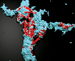
The proportion of ZnO and Fe2O3 particles in the agglomerate can also be determined. In this example (Figure 7), the results on the projected surface show a proportion of ZnO particles three times higher in area (13.88% versus 4.288%) than that of Fe2O3 particles.

Figure 7: Analysis performed on EDS maps showing projected area of each element (zinc in blue, iron in red).
Discussion
In this paper, we independently discriminate two populations of nanoparticles within an agglomerate by combining measurements from several instruments. The ultimate aim of this type of experiment is to measure particles in mixtures independently, type by type, even if the particles are similar in size and shape.
This preliminary work clearly shows that this kind of study involves critical steps:
• A real effort must be made with regards to sample preparation. Ideally, the particles must be dispersed on the substrate homogeneously. This is particularly true if the mixture is extracted from commercial products, due to agglomeration issues and the presence of residues.
• A system must be employed to easily locate the same area of the sample across a set of different instruments.
• During the imaging, the sample must not be degraded. In particular, contamination occurring during SEM and EDS analysis can be a critical issue. Preventing this phenomenon by plasma cleaning, for example, is essential.
• Obtaining EDS maps of nanoparticles requires the detector to work at very low voltage for lateral resolution issues. Drift correction during all phases of acquisition is indispensable.
• A software program allowing the colocalization of images from different instruments is required. Not only must this software allow basic correction operations on each layer of the correlated data, but it must also offer correction of relative distortions between the correlated images: ultimately, the software must be capable of handling the dataset thus created, that is, manage multi-layer images in the same way as single-channel images.
Conclusions
The proof of concept presented here shows that it is possible to discriminate nanoparticles by their chemical composition within a mixture and thus measure them independently. This achievement was accomplished by use of a combination of AFM/SEM/EDS data and the appropriate software tools. Here we demonstrate extraction of the proportion of Fe2O3 and ZnO nanoparticles within an agglomerate. In the near future, it will also be possible to extract dimensional properties of each nanoparticle population measured in a mixture by data correlation.


