


Introduction
Laser-assisted atom-probe tomography (APT) enables the acquisition of tomographic information on the elemental and isotopic composition of a broad range of specimens with near atomic-level spatial resolution and single-atom analytical sensitivity [Reference Seidman and Stiller1, Reference Kelly and Larson2]. New generations of aberration-corrected scanning transmission electron microscopes (S)TEM have led to the study of the structure and composition of different types of samples at sub-nm scale [Reference Muller3–Reference Lovejoy5]. The complementary use of both (S)TEM and APT is a powerful approach to generate detailed structural, chemical, and isotopic information on the near atomic scale. Correlative (S)TEM and APT studies show the synergies of the two methods in the study of grain boundaries, inclusions, impurities, segregation effects, defects, partitioning of elements, and phase transformations [Reference Krakauer and Seidman6–Reference Rout14]. This has been further enhanced by employing focused ion beam scanning electron microscope (FIB-SEM)-based specimen preparation techniques, which have facilitated site-specific studies of regions of interest (for example, inclusions, grain boundaries, heterophase interfaces). Additionally, various procedures have been developed especially for preparing site-specific specimens for correlative (S)TEM and APT studies [Reference Herbig12, Reference Thompson15–Reference Felfer18], where the emphasis has been on methods to minimize sample damage during the (S)TEM and APT studies [Reference Herbig12, Reference Gorman17, Reference Felfer18]. In this article we extend those works by adding an improved specimen preparation technique that reduces the use of focused-ion-beam-induced deposition of organo-metallic materials and also leads to very low sample damage during correlative (S)TEM and APT analyses.
Organo-metallic deposition is frequently used in a FIB-SEM instrument to deposit different materials (for example, Pt, W, C) to form bonds between the FIB lift-out specimen and its supporting substrate (for example, Si posts, sharpened Cu or Mo grids, SiN films). This is done in order to produce mechanically stable specimens for APT analyses [Reference Thompson15, Reference Miller16]. However, the bond produced during the organo-metallic (C, Pt, and W) deposition will be weak if the deposited connecting material is not sufficiently homogeneous. Also these bonds are usually susceptible to fracture during APT analysis, particularly in experiments that employ high applied voltages to induce field evaporation of atoms from the specimen. To alleviate issues related to weak bonding between the specimen and the substrate, we have tested and successfully employed SemGlu (Kleindiek Nanotechnik) as an alternative bonding material. SemGlu is a high-vacuum-compatible polymer adhesive that hardens under intense electron beam irradiation and is also a good electrical conductor [Reference Giannuzzi and Stevie19].
To illustrate this new methodology, we present in this article an example of the preparation method used for a specimen of Bristol iron meteorite and two steel specimens. We recently published a detailed (S)TEM and APT study of the kamacite (ferrite)-taenite(austenite) mineral interface in the Bristol iron meteorite, three analytical steel standards, and the North Chile meteorite using the SemGlu method [Reference Rout13, Reference Rout14].
Materials and Methods
Alloy specimens
To demonstrate this new procedure, we used a specimen of Bristol iron meteorite (ME 2248; Figure 1a) from the Field Museum of Natural History in Chicago and two well-characterized steel specimens from Analytical Reference Materials International (ARMI): CRM 182C and IARM 341A. The CRM 182C standard contains 2.80±0.03 wt% Ni and 0.171±0.004 wt% Co; the IARM 341A standard contains 7.16±0.03 wt% Ni and 4.44±0.02 wt% Co. For detailed compositional information, please refer to [Reference Rout14]. Initial FIB lift-outs were extracted from the kamacite (ferrite) region of the meteorite sample (Figure 1b), and the steel specimens were produced using the site-specific lift-out procedure [Reference Miller16] as routinely done for conventional TEM lamella preparations [Reference Giannuzzi and Stevie19]. A Zeiss 1540 XB FIB-SEM at the Center for Nanoscale Materials at Argonne National Laboratory (ANL) was used for this step. The composition of the standard-steel specimens were acquired from the ARMI database and were also measured with wavelength-dispersive X-ray spectrometry (WDS) using an INCAWave spectrometer on a TESCAN LYRA3 FIB-SEM at the University of Chicago. An operating voltage of 20 kV and a beam current of ~9 nA were used. Pure Fe, Ni, and Co metals and a synthetic calcium phosphate were used as standards, and counting times for peak and backgrounds measurements were 30 seconds for Fe and Ni, 40 seconds for Co, and 60 seconds for P.
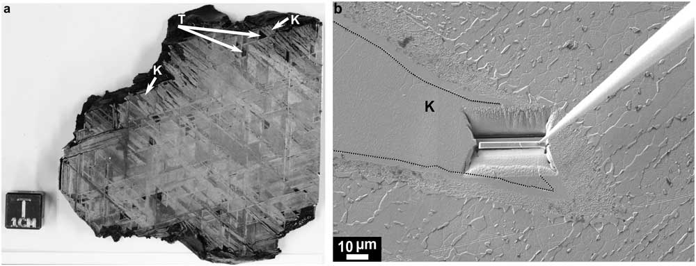
Figure 1 (a) Photograph showing the Widmanstätten pattern on an etched section of the Bristol iron meteorite (FMNH ME 2248). The plates of kamacite or ferrite (K) that grow with habit plane parallel to the (111) octahedral planes of the parent taenite or austenite (T) phase are marked with arrows. (b) SEM image of a region from the Bristol iron meteorite shown in (a). The interface between the kamacite and the taenite region is marked with dotted lines. Here a lamella is being extracted from the kamacite-taenite interface.
Half-grid preps
Independent of the above, copper TEM lift-out half grids with 5 posts (Omniprobe Lift-Out Cu 5 posts) were electropolished using 10% perchloric acid for 20–30 sec, until a 20–30 µm apex radius was achieved [Reference Baik9]. The electropolished half grids were attached to half grid holders (Figure 2a) from Hummingbird Scientific Instruments. These grid holder tips were fabricated to facilitate loading into a FIB-SEM stage, a TEM holder, and the atom probe tomograph without the need for removal of the grids from the tip. This lowers the risk of specimen damage considerably as has been reported in other studies [Reference Herbig12, Reference Gorman17, Reference Felfer18].
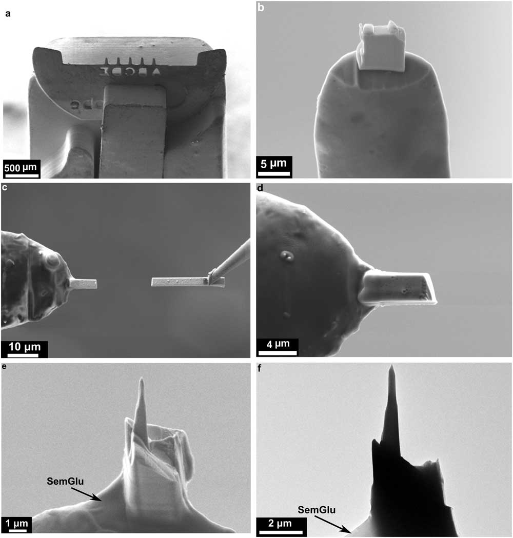
Figure 2 SEM images showing the sample preparation steps for making a nanotip for APT. (a) SEM image of the five presharpened copper microposts on a TEM half grid attached to a Hummingbird Scientific tomographic holder. (b) SEM image showing an extracted lamella attached to a copper post when the copper half grid is placed vertically inside the FIB-SEM and after the SemGlu was cured by scanning with a 5 keV electron beam. (c) SEM image showing lamella attachment when the copper half grid is placed horizontally inside the FIB-SEM. (d) Attached lamella after curing the SemGlu using 5 and 20 keV electron beams. (e) Backscattered electron SEM image showing final sample shape after high-keV and low-keV annular milling. (f) Bright-field TEM image of the nanotip showing the final tip and the base of the lamella with SemGlu.
Adhesive bonding
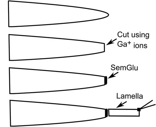
Once the lamella was lifted out of the bulk meteorite, using an in situ micromanipulator, it was attached to the electropolished Cu grid using SemGlu (Figure 2). SemGlu is a high-vacuum-compatible adhesive that has a conductivity similar to that of carbon tapes used for grounding of routine SEM samples [Reference Volbert20–Reference Martin22]. The specific advantage of SemGlu in this situation is that its hardening/polymerization can be greatly accelerated under intense electron beam irradiation (1–1.5 nA, 20 keV). Electron imaging in the FIB-SEM under conditions of low beam current (<100 pA, 5 keV) does not induce polymerization. This enables routine manipulation of the specimen to the target area on the grid using in situ micromanipulators prior to complete hardening/polymerization [Reference Volbert20–Reference Martin22]. For APT specimen preparation, the glue was first applied to the electropolished posts of the half grid (or flat-top Si microtip arrays) with a sharp needle. This procedure was done under a light microscope manually or by using a micromanipulation setup (Figure 3) external to the FIB-SEM. Care must be taken to only apply a very minimal amount of glue onto the post (for example, as a thin surface film) because excess glue can adversely affect later steps in the FIB-SEM and (S)TEM (see below).
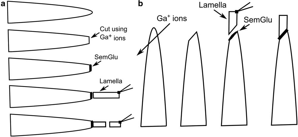
Figure 3 (a) Schematic diagram illustrating the APT nanotip sample preparation steps in a FIB-SEM using SemGlu when the sample lamella is attached horizontally onto a presharpened Cu post of a half grid. The presharpened Cu posts are shaped using Ga-ions prior to deposition of SemGlu. Once the lamella is attached, the contact region of SemGlu and lamella is scanned with a 5 keV electron beam. After 1–2 minutes of scanning, the lamella can be cut off to attach on another post. Finally, the SemGlu is completely cured by scanning around the base of each attached lamella using a 20 keV electron beam. (b) Schematic diagram illustrating the APT nanotip sample preparation steps in a FIB-SEM using SemGlu when the lamella is attached vertically on a presharpened Cu post of a half grid. The top of each post is milled with Ga-ions prior to deposition of SemGlu. Procedures for attachment of lamella and curing of SemGlu are as explained in (a).
Attaching the lamella to the post
The grid and holder was then placed either horizontally or vertically into the FIB-SEM (Figures 2 and 3). We have found that it is typically easier to orient an interface or grain boundary parallel to the vertical axis of the flat-top or electropolished grid post if the lamella is attached horizontally to the grid posts. In addition, prior to careful application of SemGlu onto the Cu posts, the Cu posts were cut using the FIB to produce a flattened top as illustrated in Figure 3. Once inserted into the FIB-SEM, the instrument’s micromanipulator was used to position the lift-out lamella close to the electropolished posts (Figures 2 and 3a). This step is done at relatively low magnification, low acceleration voltage (that is, 5 kV), and low electron beam current (<0.1 nA) in electron imaging mode, so as not to polymerize the SemGlu. Horizontal attachment of the lamella (Figures 2c–d and 3a) makes it easier to irradiate the SemGlu region with the electron beam.
Curing the adhesive
Once the lamella was in contact with the electropolished posts, the glue was cured in multiple steps by first irradiating only the region where the lamella is attached to the post using a rectangular scanning window at high magnification (50,000×), a short beam dwell time (0.5 µs/pixel), 5 kV, and beam currents of 1–1.5 nA. The specific rectangular scanning area and magnification employed depends on the size of the specimen. We have found that rastering the beam for 1–2 minutes with 1 nA current generally results in a strong bond. The lamella can then be subsequently cut with the ion beam (Figures 2c and 3). Other slices from the lamella may be attached to the remaining free posts. In a second curing step, a high-beam-current raster was scanned over the interface between the specimen and the SemGlu for 1–2 minutes at similar magnification and dwell time but at high acceleration voltage (20 kV) and higher beam current (1–1.5 nA) to complete the curing of the SemGlu. After the second curing step, the sample was rotated 180 degrees to cure the SemGlu-sample interface that is on the reverse side. This is an important step to ensure homogeneous curing of the glue and increased stability of the lamella. After final curing of the SemGlu in the above manner, the bond strength should be similar to regular epoxy-based glues.
Alternatively, if the lamella is attached vertically to the top of the Cu grid posts (Figures 2b, 3b), the above procedure needs minor modifications to achieve optimized sample attachment. In this case, prior to applying the SemGlu onto the Cu posts, the posts are milled using the FIB as illustrated in Figure 3b. Here, the base of the lift-out lamella has a similar configuration as the top of the milled posts, providing the ideal geometry for the attachment (Figure 2b, 3b). Again, once the lamella touches the top of the post, the electron beam should be selectively rastered over the specimen-glue interface using a rectangular scanning window at high magnification and short dwell times (0.5 µs/pixel). The first step of curing the glue is done by scanning a 5 keV electron beam at high current (1–1.5nA). At times in this orientation, it may be difficult to see the interface of the specimen and the glue in the SEM scanning window. In this situation, the stage and micromanipulator should be tilted a few degrees prior to attachment of the lamella to the post for a better view and improved curing. Once the specimen is attached to the post, the same procedure of curing the SemGlu may be used as described above. Curing should be done on all sides at the base of the lamella for strong and homogeneous bonding.
Final shape of the APT nanotip
The next step of shaping is accomplished by cutting the attached specimen from the sides to shape it into a square prism (cross sections of 1 µm×1 µm) using a 500 pA Ga-beam current and milling into a pyramid shape (height of 1 µm) with an apex cross section of 300 nm×300 nm using a 50 pA current [Reference Felfer18]. The final two steps of annular milling were performed with a 5–10 pA/10 kV Ga-beam to bring the sample to its final needle shape, followed by cleaning with 50 pA/5 kV Ga ions (Figures 2e–f).
Analytical transmission electron microscopy
(S)TEM imaging together with energy dispersive X-ray spectroscopy (EDS) was conducted using an FEI Tecnai F20ST field emission (S)TEM equipped with an EDAX Apollo XLT silicon-drift EDS system and a STEM-HAADF (high-angle annular dark-field) detector. For X-ray quantification, a nanotip prepared from the North Chile meteorite (Field Museum specimen ME 2595) was used for measuring the k-factors [Reference Zaluzec23] of Fe and Ni using the Cliff-Lorimer ratio method [Reference Cliff and Lorimer24] and the parameterless method [Reference Van Cappellen25]. North Chile meteorite has homogenous kamacite composition and is therefore commonly used as a standard [Reference Wasson26]. The kNiFe value determined was 1.3±0.03 at 200 kV. To improve the precision, total counts of > 100,000 were obtained for the Fe peak and total counts of > 10,000 were obtained for minor elements (Ni and Co) in measuring the North Chile meteorite standard and the kamacite nanotips. Background under the peaks was subtracted manually using the routine within the TEAMTM EDS analysis software as explained in [Reference Eggert27].
Atom Probe Tomography
A Cameca LEAP 4000X Si at Northwestern University Center for Atom-Probe Tomography (NUCAPT) with a straight flight path of 90 mm was used for all APT observations. All the APT analyses were conducted in laser mode with a pulse frequency of 250–500 Hz, using UV laser pulse energies ranging from 20–33 pJ with maximum DC voltages of 13 kV. The sample base temperature was kept at 30–35 K.
Results
Alloy standards
The APT atomic reconstructions of the nanotips prepared from the IARM 341A and CRM 182C steel alloy standards show few carbide inclusions and a Ni-rich region near the apex of the nanotip, respectively (Figure 4). The measured elemental concentrations from the APT mass spectra of IARM 341A and CRM 182C specimens did not match with the reference compositions measured using other analytical techniques (for example, SEM-WDS and optical spectroscopy data from ARMI). This is because the volumes sampled by the APT nanotips were smaller than the length scales of compositional heterogeneities within typical steel samples. For detailed information about the steel samples and other reference specimens refer to [Reference Rout14].
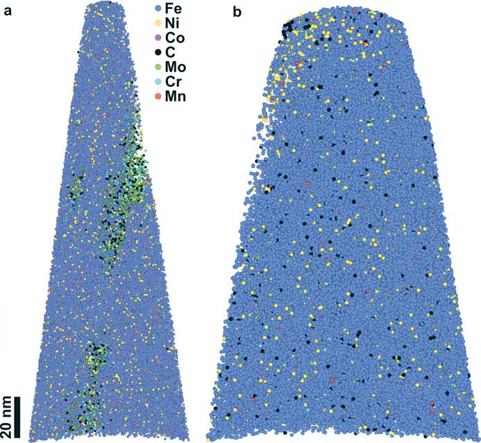
Figure 4 (a) APT reconstruction of the nanotip prepared from the steel standard IARM 341A. (b) APT reconstruction of the nanotip prepared from the steel standard CRM 182C. Each sphere represents a single atom that was detected. Only 5% of the detected atoms are shown for better illustration of the element distributions.
Bristol meteorite
Figure 5a shows the TEM image of a nanotip (Tip B) prepared from the kamacite region of the Bristol iron meteorite. Kamacite was identified first from its TEM selected area electron diffraction pattern (α-iron; ferrite; bcc; Figure 5a insert) and also from its composition measured using STEM-EDS X-ray elemental analysis: Fe=93.5±0.2 wt%, Ni=6.5±1.4 wt%. Another nanotip (Tip C) prepared from a different kamacite region had a composition of: Fe=94.1±0.2 wt%, Ni=5.9±1.4 wt%. The average Ni content in kamacite varies from ~5 wt% to ~10 wt% and depends on the cooling rates of the meteorite [Reference Goldstein28]. Within a kamacite crystal the Ni concentration is nearly homogeneous, but the Ni content decreases near the kamacite (ferrite)-taenite (austenite) interface because of the slow diffusion at low temperatures (< 350°C) during the formation of the Widmanstätten pattern [Reference Goldstein28]. Although, kamacite has on average <1 wt% Co, the concentration of Co in our nanotips could not be measured by STEM-EDS because of a small Co systems peak from the objective lens pole piece.
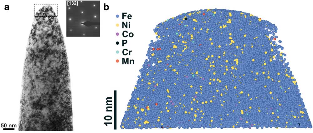
Figure 5 (a) Bright-field TEM image of a nanotip (Tip B) prepared from a kamacite region in the Bristol IVA iron meteorite. The region that was analyzed by APT is shown by a dashed box. Inset shows the selected area electron diffraction pattern acquired from the nanotip. (b) 3D APT reconstruction of the nanotip where each sphere represents a single atom. Only 5% of the detected atoms are shown for clarity. The APT reconstruction does not match with the shape of the studied region in the TEM image because some of the field-evaporated atoms were not captured by the detector during the APT analysis.
The APT reconstruction and elemental data revealed that the kamacite phase contained about 94 wt% Fe as expected for this phase, and all elements (Fe, Ni, Co, P, Cr, and Mn) were uniformly distributed throughout the nanotip (Figures 5b, 6). The composition measured from the APT mass spectrum of Tip B was: Fe=93.8±0.4 wt%, Ni=5.9±0.5 wt%, Co=0.27±0.05 wt%, P=0.024±0.004 wt%, and Cr=0.009±0.004 wt% (2σ). For Tip C the measured composition was: Fe=94.3±0.4 wt%, Ni=5.14±0.50 wt%, Co=0.49±0.05 wt%, P=0.028±0.004 wt%, and Cr=0.020±0.004 wt% (2σ). This is the expected composition for kamacite [Reference Goldstein28], and detailed information about the APT data processing and error estimation is discussed in [Reference Rout14]. The composition of the kamacite nanotips were found to be homogeneous compared to the steel-standards used in our study. This is because kamacite does not transform to any other phase at low temperatures (< 400°C) during millions of years of cooling within the iron meteorite parent body. During the formation of the Widmanstätten pattern, Ni diffuses out of kamacite into the taenite phase, and the diffusion of Ni is fast enough during the slow cooling process to produce a homogenous Ni concentration in the center of the kamacite plate. A detailed discussion about the formation of Widmanstätten pattern can be found in [Reference Yang and Goldstein29].
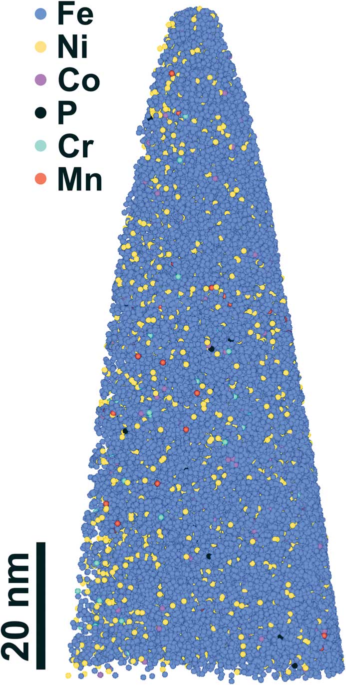
Figure 6 APT reconstruction of the nanotip (Tip C) prepared from a kamacite region in the Bristol IVA iron meteorite. Only 5% of the detected atoms are shown for clarity.
Discussion
One of the disadvantages of using SemGlu is the possibility of enhanced carbon contamination during (S)TEM work. However, the following precautions have been found to reduce the magnitude of carbon contamination. It is important that the analyst maximizes the distance between the apex of the nanotip and the base of the specimen, where the SemGlu bond is located. We have found that the distance between the nanotip and the attachment area should be greater than 5 µm to decrease the carbon contamination significantly. Also, the SemGlu must be efficiently cured, using a 20 keV electron beam, all around the base of the specimen where the SemGlu is present. If no (S)TEM analysis is required prior to APT, smaller specimens with lengths of 3–4 µm from base to apex can be used. But this is not recommended for non-conductive or dielectric samples, where laser heating must be used, because residual non-polymerized SemGlu at the base of the specimen can move to the apex of the nanotip during APT through surface diffusion. We also have observed higher peak tails in the APT mass spectra for smaller (lengths of 2–3 µm) dielectric specimens, which can be attributed to the low thermal conductivity of SemGlu. Another obvious, yet important, step is to minimize the volume of SemGlu on the Si posts and grids before attaching the specimen. Excessive SemGlu can adversely affect the specimen and sometimes leads to migration of uncured epoxy to the top of the sample by the capillary effect. Any minor carbon contamination that builds up during (S)TEM work can be removed by Ar+ plasma cleaning [Reference Roberts30]. However, for samples that are susceptible to oxidation, plasma cleaning can lead to increased rates of oxidation during subsequent storage. Care must be taken to store samples in high vacuum or in an inert atmosphere after plasma cleaning.
Conclusion
We used SemGlu as an alternative to beam-induced deposition of Pt, W, and C from gaseous organo-metallic precursors to attach the thinned lamellae onto sharpened Cu and Mo posts in Cu or Mo TEM half grids and onto flat-top Si posts. All the nanotips in our study were prepared in the FIB-SEM using SemGlu and were successfully studied with (S)TEM and APT. No sample failure occurred with APT before ~4–25 million atoms were detected. Some of the samples were stable even at high extraction voltages (~13 kV). SemGlu can therefore be used as an alternative bonding material for preparing stable nanotips both for TEM and APT studies.
Acknowledgments
The authors thank the editor-in-chief, Dr. Charles Lyman, for very helpful suggestions and corrections that improved the manuscript significantly. The authors acknowledge Sung-Il Baik for providing electropolished grids and for helpful discussions, and Betty Strack for maintaining the SEM Laboratory at the Field Museum. The local-electrode atom-probe (LEAP) at Northwestern University was purchased and upgraded with funding from NSF-MRI (DMR-0420532) and ONR-DURIP (N00014-0400798, N00014-0610539, N00014-0910781) grants. This work was supported by the National Science Foundation’s MRSEC program (DMR-1121262). We also gratefully acknowledge the Initiative for Sustainability and Energy at Northwestern (ISEN) for grants to upgrade the capabilities of NUCAPT. This research was also conducted in part at the Center for Nanoscale Materials of Argonne National Laboratory, a U.S. Department of Energy, Office of Science, Office of Basic Energy Sciences User Facility under Contract No. DE-AC02-06CH11357. PRH acknowledges the Tawani Foundation for a major grant and W. Ganz III for additional funding.


