


Introduction
High-level integration of radio frequency front-end components has the potential to yield miniaturized, cost-effective, and low loss solutions. Many modern telecommunication solutions aim toward multiple input and output (MIMO), where often a large number of antennas are implemented to increase the gain and spatial selectivity. Miniaturization of the front-end components are therefore required. As spectrum allocations and base station roll-out increase, the need for adequate band selection, harmonic and non-linear product filtering, and radio frequency interference (RFI) mitigation increases. From a system point of view, various options exist for the placement of filtering components. Adjacent placement of antenna and filter can enable final stage suppression of unwanted emissions, adequate band selection, and RFI mitigation. The integrated solution of antenna and filter is called a filtenna, where the advantages, compared to an unintegrated solution, include miniaturization, improved transition loss, direct impedance matching, and manufacturing cost reduction. Though it is not always desirable to place a passive element adjacent to the antenna due to noise figure and loss, the associated loss may be minimized through the use of high quality factor (Q) resonators.
Several published filtenna solutions are implemented using planar technologies, such as microstrip [Reference Rodrigues, Varum and Matos1–Reference Tang, Chen and Ziolkowski3] and substrate integrated waveguide (SIW) [Reference Hu, Tang, Li and Ziolkowski4, Reference Gao, Hong, Lu and Wang5]. The high Q, cost, and ease of integration with other planar components, make SIW solutions attractive for use in filtenna design. Several published filtenna works implement SIW cavities in full- or half-mode operation, single- or multi-layer structures, and with a variety of radiating elements. In [Reference Lu, Yu and Hong6], a SIW cavity-backed filtenna is presented with a stacked patch antenna configuration, while a half-mode SIW duplex filtenna with slot radiating elements is shown in [Reference Kumar and Althuwayb7]. Another slot antenna example is the SIW cavity-backed bow-tie slot filtenna shown in [Reference Mukherjee, Biswas and Srivastava9]. In [Reference Hu, Tang, Li and Ziolkowski4], a multilayered SIW filtenna is proposed in which two vertically stacked SIW cavities are integrated with a complementary split ring resonator as the antenna. The manufactured filtenna is approximately 7 × 7 cm2 and achieves a −10 dB S11 bandwidth of 6.3%, and a gain of 6.73 dBi. A single-layer SIW filtenna with parasitic patch is presented in [Reference Hu, Tang, Li, Wang and Li10], where a half-mode SIW cavity resonator is used. The manufactured filtenna is approximately $8\times 5\, {\rm cm}^2$ in size and achieves a 5.1% −10 dB S11 bandwidth and gain of 6.3 dBi at 2.77 GHz. Another single layer SIW filtenna is presented in [Reference Wang, Wang, Liu, Chen and Han11], where a slot antenna and SIW cavity are integrated. Mixed-mode coupling is used to create radiation nulls on both sides of the passband. The manufactured filtenna is approximately $2\times 2\, {\rm cm}^2$
 and achieves a −10 dB S11 bandwidth of 2.53% from 9.44 to 9.68 GHz, with a maximum realized gain of 5.8 dBi.
SIW solutions offer an improvement in quality factor compared to microstrip solutions, but at the cost of a larger size [Reference Wang, Wang, Liu, Chen and Han12]. The SIW pedestal resonator was first proposed in [Reference Nassar and Meyer13], and offers a reduction in size of the SIW resonator with Q-factors comparable to standard SIW cavity resonators. While single layer structures are possible for standard SIW resonators, the pedestal resonator requires multi-layer manufacturing. The pedestal resonator lends itself well to achieve both positive and negative coupling for coupled resonator filter design, as shown in [Reference Johnson, Meyer and Meyer14]. The pedestal resonator can therefore provide a high Q option for direct integration with antenna solutions.
This work proposes a novel SIW pedestal filtering antenna solution for use in the 5G sub-6 GHz communications. Miniaturization is achieved through integration of the radiating element into the filter design, resulting in higher order suppression. The design generates a third order filtering response utilizing two SIW pedestal resonators and one patch antenna element. The manufactured SIW pedestal filtenna achieves a ${10\, {\rm dB}}$ return loss bandwidth of 4.29% about a center frequency of ${3.63\, {\rm GHz}}$
 , and a gain of ${3.66\, {\rm dBi}}$
 . The element is also tested in a 4 element linear array configuration and a 4 element planar array configuration to demonstrate the applicability to 5G radio frequency front-ends.
An earlier version of this paper was presented at the 2022 16th European Conference on Antennas and Propagation and was published in its Proceedings [Reference Meyer, Vertegaal, Johnson, Meyer and Johannsen15]. This is an extension of the work and includes further tests on the single element, a new array configuration, and beam-scanning and dual-mode capability tests on the arrays in simulation. Details on the filtenna design is provided in Section 'Filtenna design', the prototype simulations and measurements are shown in Section ‘Filtenna prototype’, where a comparison with other published works is included. The linear and planar array setups, radiation pattern measurements, and beam-scanning and reconfigurability are provided in Section ‘Filtenna arrays’.
Filtenna design
For the initial prototype synthesis, a 3rd order Chebyshev response and in-line coupled resonator topology are chosen, with a reflection coefficient of $-10\, {\rm dB}$ . The filter $-3 \,{\rm dB}$
 band is chosen from 3.45 to 3.60 GHz for C-band operation, which is a 4.26% bandwidth about a center frequency of 3.52 GHz. The coupling matrix of the synthesized filter, obtained through Filter Designer 3D in CST, is given in Table 1, where S and L represent the source and load respectively, and the values in the first row and column represent the resonator number. For example, a bandwidth normalized coupling coefficient of 0.7631 is required between resonator 1 and 2. A positive coupling coefficient means the net field coupling is predominantly magnetic field, or inductive, coupling. A negative coupling coefficient means a predominantly capacitive coupling is required.
Table 1. Synthesized coupling matrix

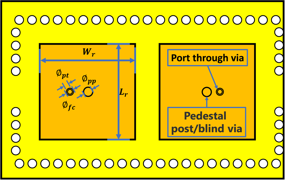
The desired response is realized by means of a SIW pedestal filtenna structure with three coupled resonators. Two resonators are SIW pedestal resonators, and the third resonator is a patch antenna element. The pedestal resonators require a multilayer stackup containing three copper layers, two dielectric (Mercurywave core) layers, and a prepreg layer (PrePreg 1080) for adhesion. The stackup is shown in Fig. 1, where the dark colors (labelled M1-3) are copper and the others dielectric or prepreg. The patches of the pedestal resonators are in the center copper layer (M2), connected to the bottom ground (M1) with one blind via each. The patch antenna is on the top copper layer (M3) with its ground on the bottom copper layer (M1). The proposed filtenna prototype, details on the center layer (M2) and vias, and the input coupling structure are shown in Figs. 2 to 4, respectively.

Figure 1. Multilayer stackup.

Figure 2. Simulated SIW pedestal filtenna.
For the connection to the antenna and a coaxial to planar transition, two planar to SIW transitions are included. The SIW cavity is formed by a single row of vias. The co-planar transmission lines couple magnetically to the SIW pedestal resonators by means of a through via, shown in Fig. 4. The pedestal resonator's magnetic field concentrates around the pedestal post, below the pedestal patch, while its electric field is maximum above the pedestal patch. The adjacent placement of two pedestals, as shown in Fig. 3, yield net magnetic inter-resonator coupling. The desired inter-resonator coupling factor between the two SIW pedestal resonators, resonators 1 and 2, is first obtained using the even- and odd-mode frequencies in the eigenmode solver of CST, which yielded 0.034 compared to the ideal 0.033 obtained when multiplying the value in Table 1 by the bandwidth.

Figure 3. SIW pedestal resonators.

Figure 4. SIW pedestal resonator feed.
Port 1 (co-planar line toward connector) is 50 Ω, while port 2 (co-planar line toward antenna) is 75 Ω. The port 1 loaded quality factor is extracted and confirmed from the CST frequency domain solver using the group delay. The extracted value for the loaded quality factor at port 1 is 35.10, while the ideal case based on Table 1 is 36.45. The port 2 via, 75 Ω line, tapered line, and antenna together form an inverter, resonator and load for the 3rd order Chebyshev response. The dimensions are found iteratively, since the final resonator and load are both due to the patch antenna and cannot be separated. The patch corners are rounded to provide a slightly wider resonance bandwidth of the antenna resonator. A patch with a narrower bandwidth causes rounding of the passband edges of the integrated filtenna response. This is due to the matching circuit limitation (Bode-Fano criteria). Compared to a standard patch antenna, this design enables improvement in roll-off characteristic. Using group delay tuning and Filter Designer 3D, which extracts the coupling matrix values from the simulated S-parameters, the SIW pedestal filtenna model is realized. Figure 2 in combination with Table 2 show the external dimensions of the designed filtenna.

Filtenna prototype
Five filtennas were manufactured by TraX Interconnect. Two of the manufactured filtennas, with edge-mount connectors, are shown in Fig. 5. Due to tolerance on the manufactured height, a slight shift in frequency, from 3.52 GHz to 3.63 GHz, and de-tuning occurred. The de-tuning is mainly due to the use of different resonator types which have different sensitivity to height change, in other words, the path antenna tunes at a different rate to that of the SIW pedestal resonators. To confirm the height change of 0.08 mm (thicker), one of the manufactured filtennas was cut to remove the antenna, leaving only the two SIW resonators, a 50 Ω input and 75 Ω output. The cutting plane is shown on Fig. 2. A 50 Ohm SMA connector is added to each port for the measurement. The simulated and measured results of the cut filter, including height compensation in simulation, is shown in Fig. 6. As expected, the impedance mismatch is evident in the 75 Ω port's reflection coefficient. The transmission coefficient for the cut filter section is −2.8 dB at 3.63 GHz. The agreement between the simulated and measured response confirms that including a height change of 0.08 mm in the simulated model will more accurately represent the manufactured prototype.

Figure 5. Manufactured SIW pedestal filtennas (detuned left, tuned right).

Figure 6. Simulated and measured 2nd order filter response.
Implementation of the height change in the filtenna simulations showed that 0.8 mm should be cut from the top edge of the patch to tune the filtenna. Filtenna 5 in Fig. 5 shows the cut top edge. The results for the tuned filtennas are presented in Fig. 7. Filtennas 1, 2, 4, and 5 were tuned correctly, while filtenna 3 was slightly over-tuned. The measured filtennas achieve a −10 dB bandwidth (BW) of 156 MHz (4.29%), at a center frequency of 3.63 GHz.

Figure 7. Simulated and measured filtenna response.
The radiation patterns of the two best performing filtennas (2 and 4) are measured using the setup in Fig. 8 and a waveguide probe (2.6 − 3.95 GHz). The measured and simulated radiation patterns for horizontal and vertical planes are shown in Figs. 9 and 10, respectively. The z-axis is normal to the patch antenna surface and the $0^\circ$ angle for both plots is in this direction. The antenna beam tilt of $15^\circ$
 downward in elevation, as seen in Fig. 10, is due to the top ground plane layer. The difference in ripple between the simulated and measured traces is attributed to structural differences, since the cable, connector and positioner are not included in the simulation. In terms of back radiation, the filtenna achieves a magnitude of around −19 dB for the back lobe. This is 24 dB below the maximum gain point. For the side radiation, there is a maximum at $El = 135^\circ$
 which gives a side lobe level of −10.7 dB. Both these values were extracted from the simulation.

Figure 8. Filtenna measurement setup.

Figure 9. Filtenna H-plane normalized radiation pattern.

Figure 10. Filtenna E-plane normalized radiation pattern.
A summary of the performance of the measured and simulated filtenna is provided in Table 3, where the gain is determined at boresight using the three antenna method. A measurement probe (WR-284) and two different manufactured SIW filtenna elements (filtenna 2 and 4) are used. It should be noted that this is not the maximum gain point, since the beam is tilted down slightly. The maximum gain may be approximated using the radiation pattern. At a downwards tilt of $15^\circ$ the normalized realized gain is 0.5 dB higher, which means the maximum gain is approximated as 4.16 dBi, while the simulation yields 4.43 dBi.
Table 3. Filtenna performance comparison

While a commonly used patch antenna has a typical gain of 5–8 dBi [Reference Balanis8], the filtenna achieves 4.43 dBi in simulation. Simulating the filtenna's patch antenna element alone, fed with a discrete port, gives a gain of 6.44 dBi. Recalling that the cut SIW filter structure has a transmission coefficient of −2.8 dB, as shown in Fig. 6, an unintegrated solution would therefore yield a gain of 3.6 dBi. However, a higher gain is achieved in both simulated and measured case for the filtenna, due to the integrated design and functionality.
As an extension to the previous work, the gain as a function of frequency is measured. The simulated and measured case is plotted in Fig. 11. To increase the simulated model accuracy, the connector is added. The measurement is made on filtenna 2. Compared to the simulation, the measured realized gain shows a slight frequency offset, but a similar behavioral profile versus frequency. This frequency offset is also visible in the filtenna response as seen previously in Fig. 7. Here, for filtenna 2, the edges of the S11 also have an offset compared to the simulation model.

Figure 11. Filtenna realized gain vs. frequency.
However, there are some points in which the measurement is performing better, achieving a gain that is up to 0.32 dB higher than the simulation, including consideration for the frequency shift. This difference in gain is attributed to several factors. First, the maximum gain is not toward boresight, but at the aforementioned −15 degrees in elevation. Given a difference in measured gain of 0.34 dB between the boresight and −15 degree points, an upward tilt error of less than 15 degrees during the measurement could have resulted in a higher measured versus simulated gain. This upward tilt error likely resulted from overcompensation for cable tension pulling the top of the antenna forward. Another factor, albeit seemingly smaller, is the measurement tolerance while determining the distance for the three antenna method. Furthermore, there will also be an amplitude variation due to cable movements for measuring the path loss. These measurement tolerance estimations are shown via the shaded area in Fig. 11, representing a 0.5 dB error. A summary of the gain vs. frequency results is given in Table 4. The difference in the simulated gain versus what is shown in Table 3 is due to the connector addition. There is a slight difference between the center frequency and bandwidth when calculated using the −10 dB points in S11 versus using the −3 dB points in Fig. 11, evident from the difference between Tables 3 and 4. This can be attributed to the rounding of the edges in Fig. 11 and the asymmetry in S11 as shown in Fig. 7.
Table 4. Filtenna gain vs freq performance at boresight comparison

A comparison between published filtennas and this work is given in Table 5. Frequency, bandwidth, gain and size are provided. In this case the data in Table 3 is used for the SIW pedestal filtenna. It is clear that a competitive size is achieved, but the gain is lower than the cited works. While [Reference Hu, Tang, Li and Ziolkowski4], [Reference Wang, Wang, Liu, Chen and Han11],and [Reference Lovato and Gong16] utilize slot antennas, [Reference Hu, Tang, Li, Wang and Li10] implements a patch antenna. This work, [Reference Hu, Tang, Li and Ziolkowski4] and [Reference Lovato and Gong16] have third order filtering with two SIW resonators, while [Reference Hu, Tang, Li, Wang and Li10] and [Reference Wang, Wang, Liu, Chen and Han11] have second order responses with a single SIW cavity.
Table 5. Published filtenna comparison

Filtenna arrays
Utilizing the SIW pedestal filtenna unit elements, two different array topologies are investigated: a linear and rectangular topology. The number of elements in each array is limited to 4. The filtenna performance in terms of reflection coefficient, gain, and beamwidth in azimuth and elevation is investigated and compared with simulation. During the measurements all other ports were loaded.
Linear array
A 1 × 4 linear pedestal filtenna array is created by placing the filtennas side-by-side. The center of the elements are therefore substrate width (41.8 mm) apart, as shown in Fig. 12a, which is 0.5 mm more than half the free space wavelength at the center frequency. The measured and simulated array pattern in the vertical and horizontal plane are shown in Figs. 13 and 14 respectively. Both these figures were generated by combining the embedded element patterns.

Figure 12. SIW pedestal filtenna array configurations, (a) The 1 × 4 linear array, (b) 2 × 2 planar array.

Figure 13. Filtenna array E-plane normalized radiation pattern.

Figure 14. Filtenna linear array normalized radiation pattern (H-Plane) while scanning, using the measured (solid) and simulated (dashed) embedded element patterns.
The simulated maximum array gain is 9.3 dBi at $15^\circ$ lower than boresight. The measured −3 dB beamwidth is $22^\circ$
 in the horizontal plane and $92^\circ$
 in the vertical plane, while the simulation shows $24^\circ$
 and $70^\circ$
 respectively. The measured side-lobe level is below −12 dB versus −15 dB in simulation. The slightly higher side lobes can be explained using the (embedded) element patterns, which have a higher magnitude at the edges, as seen in Fig. 15.

Figure 15. Filtenna normalized embedded element patterns.
Investigation of the beam-steering capability of the linear array is done and the result shown in Fig. 14. The steering is achieved by combining the element antenna patterns and applying artificial weights. While steering toward 40°, the maximum magnitude is found at around 38°. This steering deviation is due to the drop-off of the embedded element patterns outside of θ < 30°.
As with the previous array result, the main beam shows good resemblance to the simulation with a maximum difference of 1 dB, whereas the side lobes are higher for the measurements. Furthermore, when steering there is a seeming offset in the measurements and simulations when comparing the zero-crossings. As the same beam steering weights are applied to both the simulation and measurements, the difference can be found in the physical location of the antennas, which has a slight difference between the idealized planar simulation of the antenna and the practical measurement. There is also a deviation between the embedded element patterns from both the simulation and measurement.
Planar array
A 2 × 2 planar pedestal filtenna array is created by placing the filtennas with connectors pointing outwards. The center of the elements are substrate width (41.8 mm) in azimuth as well as in elevation, as shown in Fig. 12b. In this paper the results for a spacing between the two rows of antennas of λ/2 (41.8 mm) is discussed. The measurements were also done for the setup without clearance between the rows (<λ/2 separation), but besides the expected decrease in scan range, there were negligible differences.
In the measurement results, as seen in Fig. 16, the synthesized radiation pattern can be seen. This is achieved by adding a phase shift of $180^\circ$ to one of the rows to achieve a single main beam toward zenith. The second mode, for the multi-mode behavior, can be seen in Fig. 17. When exciting all the ports with the same phase, two beams toward $\pm 25^\circ$
 are created. Note that the y-axis range is different between Fig. 16 when comparing with mode 1 in Fig. 17.

Figure 16. Normalized radiation pattern of 2 × 2 Array, synthesized using the measured embedded element patterns.

Figure 17. Normalized radiation pattern of 2 × 2 array of the E-Plane, synthesized using the measured embedded element patterns, showing the multi-mode behavior.
Conclusion
This work shows a novel SIW pedestal filtenna and filtenna array, operational in the C-band for 5G sub-6 GHz communications. Miniaturization of the SIW cavities is achieved through the use of coupled pedestal resonators. The design is manufactured as a multilayered PCB including blind and through vias. The performance of the filtenna is comparable to other published works and good agreement is obtained between measured and simulated results. The measured gain at boresight was determined to be around 3.7 dBi, compared to the simulations at 3.9 dBi, with extra losses that can be account for in the measurement setup. Furthermore, a 1 × 4 linear and 2 × 2 planar pedestal filtenna array is demonstrated with possible application for future research and usage in sub-6 GHz 5G communications. Both beam-steering and dual-mode have shown to be possible when the SIW pedestal filtenna elements are utilized in an array. Improvements in gain and maximum beam direction should be considered in future designs. Additionally smaller radiating elements and structures can be investigated in future work to further miniaturize the overall structure.
Acknowledgements
This project was partially funded by the European Union's Horizon 2020 research and innovation program under the Marie Skłodowska-Curie grant agreement No 860023.
Conflict of interest
The authors declare none.
 Elmine Meyer received a BSc. in electrical engineering with minors in computer science and mathematics from Fairleigh Dickinson University, USA in 2013. She obtained a PhD in electronic engineering from Stellenbosch University, South Africa in 2018. She was employed at Stellenbosch University as a Junior Lecturer from July 2015 to May 2018, and as a Lecturer from May 2018 until October 2019. She joined Eindhoven University of Technology, Netherlands as a Postdoc in Oct. 2019 and is now an Assistant Professor in the Electromagnetics group.
 Cornelis J. C. Vertegaal was born in Boxmeer, The Netherlands in 1994. He received his Bachelor and Master degree in Electrical Engineering from Eindhoven University of Technology. As part of his MSc degree, he did an internship at Curtin University in Perth, Australia. In cooperation with NXP Semiconductors, he completed his master thesis in the electromagnetics group on the design of a 5G phased array. Niels started his PhD in 2018 at Eindhoven University of Technology. His work is based around the design of a low frequency antenna system for CubeSat applications.
 Leanne Johnson Received her B.Ing (Cum Laude) in Electrical Engineering specializing in telecommunications from Stellenbosch University, South Africa in 2016. She continued there as a Master's student in 2017, and was upgraded to a PhD in October of 2018. She obtained her PhD in April 2022 and became a postdoc at Stellenbosch University.
 Petrie Meyer is a distinguished professor in Electromagnetics and Microwaves at Stellenbosch University in South Africa. He received his PhD in 1995 from the University of Stellenbosch, on numerical analysis of microstrip circuits using the Method-of-Lines, and his DEng in 2019. He is currently the Vice-Dean (Research) of the Faculty of Engineering at Stellenbosch University. He has worked actively in the fields of passive network design, optimization, and surrogate modeling, and has authored or co-authored more than 100 technical journal and conference papers. Since 2010 he has been involved in the design of microwave filters and antenna elements for the Square Kilometre Array (SKA) radio astronomy antenna, and the South-African precursor telescope, MEERKAT. He serves as regular reviewer for IEEE, IET and Wiley microwave journals. In 2009, he was elected Fellow of the South African Institute for Engineers.
 Ulf Johannsen received his Dipl.-Ing. degree in Communications Engineering from Hamburg University of Technology (TUHH, Germany) in 2009. In 2013, he obtained his PhD in Electrical Engineering from Eindhoven University of Technology (TU/e, the Netherlands). From 2013 until 2016 he worked as Senior Systems Engineer at ATLAS ELEKTRONIK GmbH (Bremen, Germany), where his role was system designer and engineering manager on autonomous underwater vehicle (AUV) systems with sonar payloads. Since 2016, he is with the Electromagnetics group at the TU/e department of Electrical Engineering, currently in the role of associate professor. His research interest is focused on integrated antenna systems. Moreover, in 2021 he also joined the Smart Frontend group at the Netherlands Institute for Radio Astronomy (ASTRON) as senior researcher. Dr Johannsen was the coordinator of TU/e's Centre for Wireless Technologies’ (CWTe) ultra-high data-rate program and is the chairperson of the IEEE Benelux joint AP/MTT chapter.


 Open access