

I. INTRODUCTION
Wireless power transmission (WPT), electromagnetic energy harvesting (EEH), and passive radio frequency identification (RFID) are three complementary technologies in the context of Internet-of-Things era [Reference Duroc and Andia Vera1, Reference Carvalho2]. A particular case that exploits WPT is the passive RFID technology, being so far not limited to identification but extends to sensing applications. This evolution transforms the RFID into a cornerstone technology for the ubiquitous wireless sensor networks. Regarding WPT operation, the element responsible of harvesting electromagnetic energy and converting it into direct current (DC) power to feed a battery-less device and/or attached sensor is the rectifier antenna, commonly named in the literature as rectenna [Reference McSpadden, Yoo and Chang3].
Designs of these rectifying antennas for WPT and EEH are widely explained in the literature for a single-frequency band [Reference Walsh, Rondineau, Jankovic, Zhao and Popovic4, Reference Strassner and Chang5], dual-frequency band [Reference Hwann-Kaeo and I-Shan6, Reference Sun, Guo, He and Zhong7], or even for wide frequency band [Reference Collado and Georgiadis8, Reference Boaventura, Collado, Carvalho and Georgiadis9]. Most of the rectennas are designed at the Industrial Scientific and Medical (ISM) band, Global System for Mobile Communications (GSM) band, Universal Mobile Telecommunications System (UMTS) band, or millimeter wave band. However, regardless the frequency of these designs, only little attention has been paid the harmonic power generated by the rectennas [Reference Ladan and Wu10].
Indeed, the harmonic production phenomenon is generated by the rectifying operation of the circuit composed by non-linear devices. The phenomenon can be defined as harmonics in WPT (H-WPT). The architecture of rectifier circuits is based on the Cockcroft-Walton topology, with two or more diode-based voltage-doubler stages. The study case presented in this paper focuses on a similar architecture found in passive UHF RFID tags. Actually, the tag antenna is loaded by an integrated circuit, hereinafter called RFID chip. One of the tasks that the RFID chip performs is precisely the rectification operations that convert the alternating current (AC) of the RF waves sent by the reader into a DC power, thus allowing the chip to perform its other duties as transponder. These diodes determine the non-linear behavior of rectifier circuits, or RFID chips in this paper [Reference De Vita and Iannaccone11–Reference Andia Vera, Duroc and Tedjini13]. Figure 1 highlights the rectenna section as part of the passive RFID tag architecture. Three common parts for all WPT devices can be distinguished in the rectenna section: (1) the antenna, (2) the N-stage rectifier circuit, and (3) the antenna-rectifier impedance matching network.

Fig. 1. Passive RFID tag architecture. A traditional rectenna section makes part of the tag.
This paper reviews the state-of-the-art of H-WPT in the passive UHF RFID case and the possible exploitation of the wasted energy naturally produced during the rectification process performed by the RFID chip. Theory behind the harmonic generation as well as the characterization methods to evaluate the non-linear phenomena are presented.
In the application part, the power contained in the harmonic signals produced by RFID chips is used to preserve the energy-harvesting concept. The idea is to introduce diversity in frequency into the traditional operation of passive UHF RFID tags by profiting from the harmonic power to increase the harmonic backscattering. The optimized design of a dual-band RFID tag antenna, which radiates the fundamental signal and a harmonic signal, is presented and results are discussed.
Section II explains the harmonic production phenomena present in the WPT operation of passive RFID tags, and unfolds two characterization methods used to evaluate its non-linear behavior. Section III presents the application example by designing a dual-band tag antenna to implement diversity in frequency. Experimental results are also discussed. Finally, in Section IV some conclusions are drawn.
II. HARMONICS IN PASSIVE UHF RFID
Although rectennas used for EEH and passive RFID tags have similar RF section, there is a small but crucial difference on the non-linear treatment. Because of the non-linearity behavior of the diodes used in the rectifier, appropriate techniques of simulation and optimization are used in those circuit designs. The harmonic balance (HB) is a simulation method that considers the effect of the harmonic currents produced by non-linear devices [Reference Georgiadis, Andia Vera and Collado14]. In the rectenna case, the RF currents flow to the DC section and to antenna terminals. If they are well filtered in the DC section side, a good DC signal can be achieved at the output, and then an enhanced RF-to-DC conversion efficiency is obtained [Reference Georgiadis, Andia Vera and Collado14–Reference Falkenstein, Roberg and Popovic16]. The phenomena can be simulated with the HB method, being possible to predict and to control the behavior of the complete rectenna, both in the DC section and in the antenna. In passive UHF RFID chips, the harmonics reflected through the DC section are surely treated in the process of chip design, and then an optimal DC signal feeds the digital section of the chip. However, the harmonics are reflected through the antenna since no harmonic treatment consideration is performed on the RFID antenna design. Antenna design in passive RFID tags begins directly from the knowledge of the chip impedance at the fundamental frequency provided by data sheets [Reference Finkenzeller and Muller17, 18]. Summarizing, the design process aims to ensure impedance matching at the frequency of operation, but the antenna-chip matching behavior around harmonic frequencies is unknown. As long as antenna and chip are independently designed [Reference Finkenzeller and Muller17, Reference Paret19], the antenna can radiate some of the harmonic currents generated by the rectifier, which finally triggers in harmonic backscattering [Reference Andia Vera, Duroc and Tedjini13, Reference Nikitin and Rao20].
Figure 2 shows the harmonic current distributions on a half-wave dipole antenna structure operating at fundamental frequency. For traditional RFID tag antennas based on half wave dipoles it should be noted as expected, that odd harmonic responses will be higher compared to even ones.

Fig. 2. Current distribution until 5th harmonic along the length of a half-wave dipole designed for fundamental frequency [Reference Andia Vera, Duroc and Tedjini13].
To perform a qualitative analysis about the power strength of harmonic signals produced by passive RFID chips, specific characterization methods are needed.
Several characterization platforms for passive UHF RFID have been proposed in the literature. For example in [Reference Chen and Lin21–Reference Nikitin and Rao27] techniques to evaluate the performance of chip–antenna integration are proposed, contrary to [Reference Chen, Lin and Mittra22, Reference Catarinucci, De Donno, Guadalupi, Ricciato and Tarricone25–Reference Nikitin and Rao27] the impedance matching is strictly evaluated. In [Reference Catarinucci, De Donno, Colella, Ricciato and Tarricone23–Reference Nikitin, Rao, Martinez and Lam26] techniques to measure the differential radar cross-section (ΔRCS) and sensitivity of RFID tags are proposed.
In this paper, two characterization methods to evaluate the strength of harmonic signals in passive RFID are discussed. The first one is based on radiated measurements performed over complete RFID tags, the second one is based on conducted measurements performed directly over RFID chips. The methods are valid to perform accurate measurements in a wide frequency range including harmonics, and having the chip activated.
A) Radiating measurements
1) Setup, methods, and metrics
A technique used to characterize the harmonics produced by passive UHF RFID tags was presented in [Reference Andia Vera, Duroc and Tedjini13]. The analysis procedure of harmonic responses is based on radiated measurements. The RFID communication between the RFID test-bench and the tag is established and simultaneously, a power spectral density (PSD) analysis is performed over time domain communication signals. The fast Fourier transform (FFT) calculation is made over the carrier wave (CW) portion after the Query command is sent. In case of tag response, the PSD analysis shows side lobes around the carrier like a typical spectrum of square waves as consequence of the modulated information. The conceptual procedure of the method is represented in Fig. 3.

Fig. 3. Conceptual procedure based on PSD analysis of UHF RFID signals [Reference Andia Vera, Duroc and Tedjini13].
One of the major contributions of the method [Reference Andia Vera, Duroc and Tedjini13] is to highlight the characteristics of the backscattering modulation to clearly interpret the time-domain signals and its PSD calculation. The PSD analysis considers the configuration of the RFID air interface to produce a periodic sequence of bits on the tag response [Reference Andia Vera, Duroc and Tedjini28]. Indeed, characteristics as backscattering link frequency (BLF), data encoding and preamble are pre-configured on the treatment of the physical layer in the UHF RFID communication. Regarding the setup, measurements were done in an anechoic chamber specially prepared for bi-static configuration offering a partition wall of 48 dB isolation between horn antennas, thus minimizing the mutual coupling. The setup is shown in Fig. 4. As a result, the passive RFID tag response level is quantified at the fundamental frequency and its harmonics.

Fig. 4. (a) Setup distribution in the anechoic chamber. (b) Equipment setup for bi-static configuration.
2) Results
The first part of the analysis measures the sensitivity from five different commercial tag inlays. Table 1 shows detailed results.
Table 1. Measured sensitivity of tags under test.

Considering each tag sensitivity, Fig. 5 shows the level of the backscatter response, for the fundamental frequency and its harmonics. In all cases, besides the fundamental frequency, the 3rd harmonic response is predominant among the remaining, reaching in the higher case −86 dBm. Representative results (2nd and 3rd harmonic) are summarized in Table 2.

Fig. 5. PSD of the tag response. The values are taken at the activation threshold of each tag at the fundamental frequency.
Table 2. Harmonics of the tag response.

B) Conducted measurement
1) Setup, methods, and metrics
An RFID Test Platform (RFID-TP) for conducted measurements performed directly over RFID chips was presented in [Reference Andia Vera, Duroc and Tedjini34]. This platform complements the radiated measurement exposed above, offering a complete non-linear characterization for passive tags. The RFID-TP enables to perform accurate measurements, when the RFID chip is activated, in a wide frequency range that includes harmonics. The main difference with respect to radiate measurements is the direct connection of the RFID chip to the measurement system RFID-TP. This technique allows the characterization of different types of chip, and avoids to consider the effect of fixed tag antenna structures. Unlike the radiated measurement method presented in Section II-A, conducted measurement includes a vectorial characterization, which is one of the major contributions of this method. Indeed, thanks to this method it is possible to measure both complex impedance modulation states (scavenging and reflecting) in a wide range of frequencies, even at the harmonic frequencies.
Regarding the composition of the RFID-TP, the block diagram setup is shown in Fig. 6. Two main parts are highlighted. The first one consists on specialized equipments for microwave measurements and named “RFID tester”. The second one is composed by two impedance tuners connected in series with the fixture that holds the RFID chip and named “antenna impedance emulator”. With the described configuration, a complete characterization can be performed under full communication between RFID-TP and chip. The setup depicted in Fig. 7 is briefly described below. Further details can be found in [Reference Andia Vera, Duroc and Tedjini34].
-
• RFID tester: An Agilent N5224A Programmable Network Analyzer (PNA) is used to generate the Query command by using an external source [35]. The external source is a Vector Signal Generator (VSG) with a 20 dB low pass filter (LPF) at its output, to ensure that the chip harmonic response is self-generated. After the Query command is sent, the PNA determines the chip impedance during scavenging and reflecting states over a temporal sweep at the frequencies of interest [Reference Andia Vera, Duroc and Tedjini13]. A Digital Storage Oscilloscope (DSO) also connected to the chip allows the visualization of the modulated response. Additionally, the PSD analysis is performed over the time window to assess the response of the chip [Reference Andia Vera, Duroc and Tedjini28]. Finally the control of the RFID-TP is made by a Matlab program running on the host PC.
-
• Antenna Impedance Emulator: It is composed by two impedance tuners connected in series to provide matching between the 50 Ω RFID tester and the chip. The RFID chips were fixed over 50 Ω SMA connectors [Reference Nikitin, Rao, Martinez and Lam26]. When the matching is achieved (by setting the tuner positions), the chip is in scavenging state and once activated, it switches between its two modulation states. Details are presented in [Reference Mayer and Scholtz36].

Fig. 6. Conducted measurements setup to characterize harmonics backscattered by RFID chips [Reference Andia Vera, Duroc and Tedjini34].

Fig. 7. Conducted measurement setup [Reference Andia Vera, Duroc and Tedjini34].
Under this operation, Fig. 8 shows an experimental example of the PSD analysis in the DSO, in a frame where the scavenging matching condition was achieved and the chip responds. The side lobes due to the modulated response are shown for the fundamental, 2nd and 3rd harmonics.

Fig. 8. Harmonic characterization method by conducted measurements [Reference Andia Vera, Duroc and Tedjini34].
2) Results
Using the conducted method described above, harmonic characterization for three commercial RFID chips is reported. The chips are (1) G2XM NXP SOT505-1 [37], (2) G2XM NXP SOT1040-AA1 [37] with strap, and (3) Impinj Monza 5 [18] extracted from a commercial inlay AKtag [38].
The harmonic response level was measured for the three chips from the fundamental frequency until the 4th harmonic, by performing the PSD analysis over the same response frame in all cases. Results are shown in Fig. 9. As already discussed in Section II-A, the 3rd harmonic is predominant for all chips under test. It is worth noting that a backscatter response is detected even at the 4th harmonic for an input power above 3 dBm in the case of chips 1 and 3. Details about the harmonic responses at the activation power are shown in Table 3.

Fig. 9. Harmonic responses measured for the three chips while sweeping the power transmitted by the RFID-TP. A characterization from the fundamental frequency until the 4th harmonic is presented [Reference Andia Vera, Duroc and Tedjini34].
Table 3. Harmonics responses from RFID chips.

Since vectorial characterization is included in this method, the measurement of the impedance modulation is possible, while the chip is activated. Figure 10 shows the input impedance of the chip 1 in both modulation states for the fundamental and its 3rd harmonic. At the 3rd harmonic, the resistive part decreases and the reactance becomes more capacitive compared with the impedance at the fundamental frequency. Moreover, the difference between both modulation states is lower which means in a radiating scenario, that the ΔRCS [Reference Skali, Chantepy and Tedjini39] will be smaller than that one at the fundamental frequency.

Fig. 10. Measured chip input impedance for the fundamental frequency and its 3rd harmonic frequency in a temporal sweep. Both impedance modulation states, scavenging, and reecting can be observed.
The characterization platforms above exposed, write down a new line on the state-of-the-art of the passive RFID technology, especially for what concerns the intrinsic non-linear phenomena that occur in WPT operations, i.e. H-WPT. With the new characterization tools, the power carried by harmonics generated by passive RFID chips is evidenced. It is worth noting that harmonic signals are also carrying the modulated information.
Hereafter, given the redundant information originated on the same chip, a new application example makes use of this energy. The design of an RFID tag antenna radiating the 3rd harmonic besides the fundamental signal is proposed.
III. APPLICATION EXAMPLE
This section presents an application example that uses the harmonic power generated by passive UHF RFID chips. The design of a harmonic tag (HT) with the following requirements is envisaged [Reference Rao, Nikitin and Lam40–Reference Virili42]:
-
• Frequency band. Dual-band operation is required: at the fundamental frequency of 915 MHz and its 3rd harmonic 2745 MHz.
-
• Structure. A direct and fast prototyping is desired. The tag will remain as simple as possible based on printed dipoles in order to exhibit omnidirectional behavior.
-
• Read range. A maximum read range is desired under the local regulations. The antenna-chip matching is optimized to ensure the tag performance. Regarding the polarization, reader and tag antennas are oriented for the maximum polarization matching.
-
• Application. It concerns on the use of the energy contained on the 3rd harmonic self-generated by a passive RFID chip. It is envisaged to enhance the harmonic backscattered level by designing a specific HT.
-
• Cost. A low-cost prototype is desired. The materials are paper substrate with relative dielectric permittivity of 2.31 and thickness of 1 mm, copper tape and an available commercial loop-shape tag.
A) Modeling
1) Single-band antenna
Initially as a comparative reference, a single-band dipole antenna (SDA) for a conventional operation at 915 MHz was designed (Fig. 11). For the conjugate impedance matching, the method of inductively coupled loop was used. The method considers a radiating dipole inductively fed via a coupled small loop [Reference Marrocco43, Reference Nguyen, Le, Pham, Nguyen, Dang and Tedjini44]. For practical reasons, the commercial AKTAG inlay tag [38] is used as inductive loop. From conducted measurements, the imaginary parts of the antenna that conjugate the impedance of the chip at fundamental and its 3rd harmonic are 148 and 39 Ω respectively, whereas the optimum real parts are approximately 15 Ω in both bands.
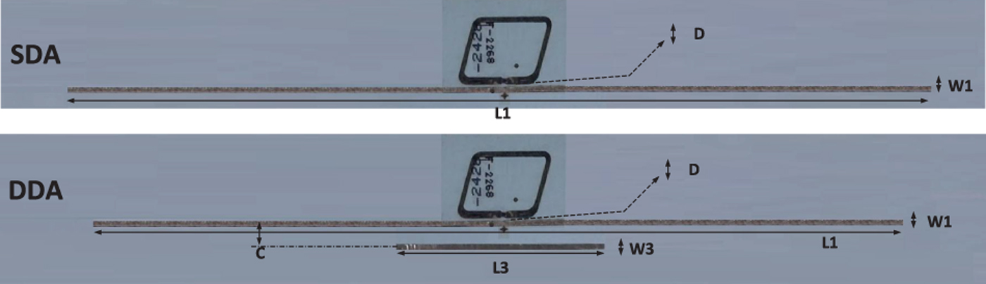
Fig. 11. SDA and DDA tag prototypes.
2) Dual-band antenna
With the purpose to enhance the 3rd harmonic backscatter signal, a second antenna called dual-band dipole antenna (DDA) was designed (Fig. 11). The DDA uses a coplanar parasitic element, which lies parallel to the driving dipole. The parasitic element and the driving dipole have different resonant lengths for the fundamental frequency and its 3rd harmonic, respectively. The parasitic element is fed by the driving dipole being at a coupling distance “C”, which yields it to the resonance [Reference Zhijiang, Ronghong, Junping and Jing45, Reference Chang, Kim and Yoon46].
3) Impedance matching considerations
The arrangement of each antenna (SDA or DDA) with the AKTAG loop, whose terminals are directly connected to the chip, adds an equivalent inductance to the antenna. The strength of coupling and therefore of the added reactance, is controlled by varying the distance between the loop and the antenna. It is important to note that the mutual coupling and therefore the total input resistance of the SDA or DDA is dependent on: (1) the loop shape that is in this case fixed and (2), on the SDA–loop distance. On the other hand, the reactance is mainly affected by the loop design [Reference Marrocco43]. The distance “C” plays a key role for the reactance and the resistance of the DDA for the 3rd harmonic frequency. The proposed designs are etched on paper substrate. The configuration of the proposed SDA RFID and DDA RFID tags is shown in Fig. 11. Table 4 summarizes all the design parameters.
Table 4. Dimensions of tags SDA and DDA.

Some basic assumptions for the simulation carried out in CST Microwave-Studio are described below:
-
• The inductive coupling and the resulting input impedance seen from the loop terminals are fixed and assumed to be optimal from the commercial AKTAG design.
-
• The DDA design was done initially separately from the AKTAG loop considering the feeding point on the middle of the driving dipole. As a second step, the loop model including its adhesive package, is introduced in the simulation with the real feeding point on the loop.
-
• To optimize the coupling DDA-loop, the distance between both elements is optimized considering the chip impedance measured at fundamental frequency and the 3rd harmonic frequency.
-
• All the electrical features of the used low cost materials were considered in the simulations.
Performance results about the SDA and DDA tags are depicted below. Figures 12 and 13 show the simulated resistance and reactance of the SDA and DDA at fundamental frequency and its 3rd harmonic, respectively. The impedance around the fundamental frequency and its 3rd harmonic are closely the conjugate of the chip impedance. Simulated return loss of antennas is depicted in Figs 14 and 15 for the fundamental frequency and its 3rd harmonic, respectively. The impedance bandwidth for the DDA at 915 MHz is 4.46%, and at 2745 MHz, it is 1.70%.

Fig. 12. Simulated input impedance for the SDA and DDA at the fundamental frequency.

Fig. 13. Simulated input impedance for the SDA and DDA at the 3rd harmonic frequency.

Fig. 14. Simulated return loss of SDA and DDA at the fundamental frequency.

Fig. 15. Simulated return loss of SDA and DDA at the 3rd harmonic frequency.
The simulated realized gain patterns in the H-plane at 915 and 2745 MHz are depicted in Figs 16 and 17, respectively, for the SDA and DDA tags. It is shown that the pattern at the fundamental frequency and its 3rd harmonic are comparatively featured more close to an omni-direction pattern. The simulated realized gains at 915 MHz and at 2745 MHz are 2.54 and 1.45 dBi, respectively.
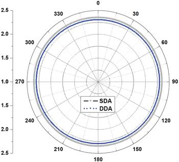
Fig. 16. SDA and DDA simulated radiation pattern at 915 MHz.

Fig. 17. DDA simulated radiation pattern at 2745 MHz.
B) Experimental results
For the prototyping of the SDA and DDA RFID tags, a technique called cutting plotter-based tag prototyping on flexible adhesive copper sheets (CPFACS) [Reference Catarinucci, Colella and Tarricone47–Reference Alimenti, Mariotti, Mezzanotte, Dionigi, Virili and Roselli49] suitable for cost-effective, time-saving, and high-performance is used. The CPFACS prototype is finally joined with the commercial loop tag.
With the radiated measurement method presented in Section II-A, the SDA and DDA tag prototypes were evaluated. Figure 18 compares the SDA and DDA tag performances at the 3rd harmonic frequency. The goal of enhancing the harmonic backscatter level is accomplished. An improvement of 15.62 dB on the 3rd harmonic backscatter level coming from the DDA is measured with respect to the SDA. The experiment confirms that the 3rd harmonic power can be efficiently radiated by properly tag antenna design. It is important to note the higher carrier level (main central lobe) for the DDA in Fig. 18. This effect stands out the impedance matching condition at the harmonic frequency, since the harmonic carrier is self-generated by the chip. Figure 19 compares the PSD of the tag response until the 5th harmonic for tags T5, SDA, and DDA. The tag DDA has a 3rd harmonic response 10 dB higher than that one coming from the tag T5.

Fig. 18. PSD comparison between SDA and DDA prototypes at the 3rd harmonic. The DDA tag presents enhanced performance.

Fig. 19. PSD comparison between the prototypes and one commercial tag until the 5th harmonic.
Two important achievements can be highlighted from the presented example: (1) the use of the commercial AKTAG loop allows us to simulate simple antenna structures, which triggers in light simulations, and fast prototyping; (2) regarding the performance of the solution, it has been demonstrated the feasibility of the harmonic energy recycling. The DDA is able to maintain a traditional RFID communication at 915 MHz with the reader, and at the same time to produce a redundant signal at its 3rd harmonic frequency. The redundant backscatter harmonic is 10 dB higher than that one from the commercial tag T5. However, the enhancement is achieved at the expense of a 6 dB reduction on the tag response level at the fundamental frequency. The impedance matching condition achieved at the 3rd harmonic degrades the matching condition at the fundamental frequency, which consequently triggers in (1) a reduction of the tag sensitivity, and (2) a reduction of its response strength, congruent with experimental results for harmonic treatments reported in [Reference Andia Vera, Duroc and Tedjini34]. Nevertheless, the global read range of the HT will be limited by the harmonic strength, which in all cases is smaller than that one at the fundamental frequency. Considering only one receptor, the global read range of the HT will depend on the receptor sensitivity at the harmonic frequency.
IV. CONCLUDING REMARKS
This paper presents novel methodologies for the characterization of harmonics generated by harvester devices and considers their application to the passive RFID tags case. The efficient treatment of harmonics signals allows us to establish a redundant communication from tag to reader in the traditional passive RFID technology. Early studies have treated the non-linearity of the RFID chip as a spurious effect while ensuring the matching between antenna and chip at certain level of power at the fundamental frequency [Reference De Vita and Iannaccone11]. It is worth noting that the non-linearity, in uncontrolled conditions, is certainly destructive and has negative impact on the performance pg the system. More recently, studies demonstrate that the non-linearity effect exists in normal operation conditions, and it generates a 3rd harmonic backscatter signal that carries information. Experimental results have shown that proper antenna design can increase the harmonic backscatter level of passive RFID tags. A new HT based on a dual-dipole antenna has increased the level of the 3rd harmonic backscatter signal by 10 dB. However, the impedance matching condition achieved at the 3rd harmonic degrades the matching condition at the fundamental frequency, resulting in a reduction of the response level at the fundamental frequency but without limiting the global performance of the harmonic tag.
In a more general analysis, the H-WPT is an intrinsic phenomenon of harvester devices that rectify RF signals. In the spirit of green power, and particularly green RFID [Reference Duroc and Kaddour50], further research efforts could be devoted to the use of the energy contained in these harmonics. In this context, the H-WPT can be rectified and used for ultra-low-power feeding.
ACKNOWLEDGEMENT
The authors wish to thank to TAGSYS RFID Company for providing us with the AKtags, and to Marc Recouly for insights and value discussions.
 Gianfranco Andía Vera He was born in Puno, Peru, in 1986. He received the engineering degree from the Escola Tècnica Superior d'Enginyeria de Telecomunicació de Barcelona – ETSETB at the Universitat Politecnica de Catalunya-UPC in 2009. He received his master degree in Development and Management on Information Technologies, in 2010 also by UPC. From May 2010 to September 2011 he worked as an engineer in a carrier telecom in Barcelona, Spain on the planning of wireless networks to distribute VoIP and IP services. In October 2011, he has joined the Laboratoire de Conception et d'integration des Systemes LCIS Valence, France where he is currently pursuing a Ph.D. diploma at the Grenoble Institute of Technology. His primary interest includes RFID, antennas, energy harvesting, wireless networks, and microwave devices.
 Yvan Duroc He received the Teaching degree Agregation (French national degree) in applied physics in 1995, the Ph.D. degree in electrical engineering from the Grenoble Institute of Technology in 2007 and the HDR degree (Habilitation à Diriger des Recherches) from the Grenoble University in 2012. He was a Teaching Associate with Esisar Engineering School from 1997 to 2009, where he was an Associate Professor from 2009 to 2013. Since 2013, he has been a Professor with the University Claude Bernard Lyon 1, France. He is In-charge of lectures in signal and image processing, electronics, RF, and embedded systems for the engineer and M.Sc. levels. His current research interests include microwave and signal processing with special attention to radio frequency identification, ultrawideband, and radio cognitive technologies. Professor Duroc is the Vice President of the URSI Commission C, France.
 Smail Tedjini He received Doctorate in Physics, from Grenoble University in 1985, and became full Professor in 1993. His main topics of interest are electromagnetism, RF, Wireless, and optoelectronics. His current research concerns wireless systems in particular RFID. He is the founder and past Director of LCIS Laboratory. Actually, he is the ORSYS group leader. He supervised more than 30 Ph.D. and has more than 300 research publications. He served as the Examiner/reviewer for tens of Ph.D. for different universities (France, Germany, Italy, Vietnam, Australia, Singapore, India, Brazil, Maghreb, etc.). He is the Member of several TPC and serves as the expert for international scientific committees and conferences, including ISO, Piers, IEEE, URSI, and EuCap. He organized several conferences/workshops. Past President and founder of the IEEE-CPMT French Chapter, the Vice-President of IEEE France Section and the Chair of URSI Commission D for the Triennium from 2011 to 2014.


