


Introduction
Collecting good data is an important task, but handling the data correctly is important also. How to handle data largely depends on what the analyst is going to do with it. Electron backscatter diffraction (EBSD) is no exception.
Electron backscatter diffraction is a widely used technique for collecting crystallographic information at micrometer and even nanometer scales [Reference Schwartz, Kumar, Adams and Field1, Reference Randle2]. An EBSD orientation map, or inverse pole figure (IPF) map, is acquired in a scanning electron microscope (SEM) by scanning the electron beam over an area of interest. An orientation map is produced by placing the beam sequentially at a series of points on the surface of the samples and performing several operations: collection of an electron backscatter diffraction pattern, detection of the lines in the pattern using a Hough transform, calculation of the orientation of the crystal based on candidate crystal structures for the specimen, and storage of this orientation information (Figure 1). The electron beam is then moved and the process repeated until a map of orientation data is complete. Currently, EBSD can be used to map crystallographic parameters such as phase type and fraction, grain size, orientation distribution, and deformation content. These measurements can be made rapidly, routinely in excess of 100 patterns per second.

Figure 1: Basic geometry and data of the EBSD experiment. A) Chamberscope image of the internal geometry of the SEM during an EBSD experiment. B) Raw EBSD pattern from silver metal. C) Overlay of indexed solution to the EBSD pattern in B.
A good example of standard orientation mapping of an iron-based, magnetic alloy is shown in Figure 2. This image represents 585,000 pixels and 95.7 percent of those pixels were successfully indexed by the software. The unindexed pixels mainly reside on grain boundaries and at second phase particles (small black areas) that were not included in the list of phases to be considered. The orientation map in Figure 2 is an inverse pole figure, and its colors are explained by the color key on the stereographic triangle. An inverse pole figure can be plotted with respect to any physical direction. Normally, either x, y, or z is chosen—the direction that has the most physical significance, for example, rolling direction, growth direction, etc. The choice of indices is based on a given stereographic triangle. Because the crystal structure in Figure 2 is cubic, the choice of a particular stereographic triangle is arbitrary. Once a given triangle is chosen, however, all of the indices must be consistent. For example, in Figure 2 the IPF was plotted with respect to the x-axis and shows the stereographic triangle with the 001, 111, and 101 poles. In Figure 2, any pixels that have a ⟨001⟩ parallel to the x-direction in the microscope (horizontal in the map) direction are colored red, those with the ⟨111⟩ direction parallel to the horizontal direction in the image are colored blue, and pixels that have a ⟨101⟩ direction parallel to the horizontal direction in the image are colored green. This image represents what we would consider to be good data, as-acquired, and we would expect that measures of grain size and orientation parameters would be reliably interpretable.

Figure 2: High-quality EBSD inverse pole figure map of a magnetic alloy (raw data). There were 585,000 patterns collected for this image with 95.7% successfully indexed. Note that many of the unindexed pixels were at grain boundaries or at second phase inclusions (black). The color key for the image (stereographic triangle) is shown at right.
Unlike most other analytical techniques in the SEM, there are pixels in the acquired data set that have no useful or reliable interpretation, leading to data maps that have missing pixels or speckled noise in them. In order to make the resulting orientation maps more visually appealing, various data-cleaning routines have been made available by the manufacturers. These algorithms may be based on sound crystallographic and microstructural reasoning, but it is easy to misapply them, resulting in data with introduced artifacts. S.I. Wright describes a particularly clear example of artifacts generated in orien-tation maps of copper interconnect lines in devices with the overuse of these algorithms [Reference Wright3]. Unfortunately, many authors perform this data modification routinely without ever mentioning the process in published papers.
This article examines two common scenarios in which EBSD data quality may create problems for the analysis and where one must be careful in doing noise reduction: unindexed pixels and systematically misindexed pixels. This article is not a review of de-noising or filtering routines, nor is it a comprehensive examination of the algorithms themselves. Instead, this article attempts to point out the potential problems with data cleaning or filtering so as to encourage EBSD analysts to think more critically about the nature of “noise” in their data before cleaning it.
EBSD Data Quality
The quality of EBSD data is measured primarily by the percentage of pixels correctly indexed. A correctly indexed pixel is one for which a calculated orientation of a proposed phase has been matched within an angular tolerance to the experimentally collected EBSD pattern. Incorrectly indexed pixels include: (1) pixels with no suitable match, an “unindexed” pixel; (2) pixels with crystallographic ambiguity in the indexing, “systematically misindexed”; and (3) pixels that have crystallographic solutions that are not reasonable, “randomly misindexed.” The overall quality of an EBSD orientation map is often measured as the percentage of correctly index pixels or “hit rate.”
The quality of EBSD data is determined by many factors: sample preparation, grain size, crystal symmetry, Debye-Waller factor (how much thermal vibration is present at a given temperature), speed of collection, etc. Simple metals, such as copper, nickel, brass, and iron, can be easily prepared metallographically and give beautiful EBSD patterns that yield high-quality mapping data. Other materials, such as zircalloy, many oxides, and some titanium alloys, can be mapped by EBSD but give lower-quality data in terms of hit rate.
The effective quality of EBSD data depends upon the analyst's use for it. For example, a data set with seventy-five percent of the pixels correctly indexed might be fine for qualitatively showing the shapes and morphologies of grains and for basic pole figure generation. However, this data set quality may not be high enough for quantitative grain-size measurements. In EBSD analysis software, one may be given the opportunity to reduce the noise in the data set until, for example, ninety-five percent of the pixels are said to be “correctly indexed.” However, if we do this noise reduction, what are the consequences on how we use the data? Can we still do quantitative grain size measurements? Are the pole figures still usable?
Problem 1: Unindexed and Randomly Misindexed Pixels
In the literature when EBSD orientation maps are presented, it is not uncommon to observe maps that are absolutely beautiful and are completely devoid of pixels that are misindexed or unindexed. In our experience, these maps seldom exist as collected from the SEM, yet in published articles they appear frequently, with no mention of any post-processing. Even with simple, well-polished samples, it is uncommon to collect data with 100 percent of the pixels correctly indexed. Unindexed pixels are often most apparent at grain boundaries where overlapping patterns cause the indexing algorithms to fail. In addition, most orientation maps have a small percentage of unindexed pixels randomly distributed throughout the map. Higher-speed data collection can increase the percentage of these pixels. There are sometimes isolated, single pixels that have an abrupt orientation change, which may be suspect for random misindexing.
The standard procedures used to clean or filter unindexed or misindexed pixels require two steps. Step one will generally remove the isolated, possibly misindexed, pixels. There are a variety of methods that the commercial manufacturers use for this process, but the result is the same. The pixels in the orientation map are inspected. Single pixels or even multiple pixel clusters below a certain size threshold are examined to determine if their orientation is consistent with their nearest neighbors in the map. If the single pixel or the cluster of pixels is found to be below a particular angular deviation (sometimes user definable), then the single pixel or the cluster of pixels is set to the orientation of the neighboring pixels. This procedure is relatively safe, provided the size threshold is not too large and, more importantly, there is not a systematic misorientation between the isolated pixel clusters and the surrounding matrix. Additionally, isolated clusters of pixels might also represent a second phase or a special orientation relationship and should be considered further by the analyst before removal.
In the second step, pixels that are unindexed are addressed. This step involves locating the pixels with no suitable indexing, examining the nearest neighbors, and then using some interpolation of the neighboring orientations to fill in the unindexed pixel. This procedure is usually completed across the entire map. The extent to which this “pixel filling” is performed is often controlled by the number of neighboring pixels required and the number of iterations that are applied. It is apparent in the literature that many authors prefer to fill in all of the unindexed pixels to present a map that is more pleasing to the eye. However, one should ask, “What can I safely say about my data after filling in these pixels?” Or “Have I changed the data to the point that I no longer am confident that it represents my sample?” Figure 3 shows the data in Figure 2 with the application of these standard procedures. Note that the initial quality of the data was already quite high with more than 95 percent of the pixels successfully indexed. After removing random misindexing and filling in unindexed pixels, the map looks pleasing to the eye but not really different from the unfiltered data with one important exception: all of the small, round, second phase particles are now gone. Were they important? We would not even know that they were present if we only presented the filtered result in Figure 3.

Figure 3: The same map as in Figure 2 with the misindexed and unindexed pixels removed, using a 6-neighbor rule, iterated 6 times. Note that none of the second phase inclusions are represented in the microstructure.
Risks of Pixel Filling. The risks of pixel filling really depend upon what the analyst wants to say about the data. Comments on the size and shape of grains, or prevalence of a particular orientation with respect to surface of the sample, are not likely to be affected by a modest amount of data filtering. However, trying to quantitatively measure the grain size or even the orientation distributions may be risky if too much of the data is “filled in” or if the distribution of unindexed pixels is crystallographically distributed, for example preferential etching of grains. See Wright et al. [Reference Prior, Mariani, Wheeler and Schwartz4] for the effects of data cleaning on orientation distributions functions.
Figure 4 shows several pixel areas with unindexed pixels. In each case, the missing pixel or pixel cluster is analyzed to determine how many neighbors and how many filter iterations are necessary to fill in the unindexed pixels. A “neighbor rule” with more neighbors and fewer iterations will have less risk of corrupting the data. The most conservative neighbor rule and the number of iterations for each example can be found in Table 1. For the area with only one orientation and one unindexed pixel, filling in that pixel can be done with an 8-neighbor rule (four nearest and four second nearest neighbors, Figure 4A) and in one iteration. The noise introduced into the data is based on the average misorientation between the 8 other pixels and is not likely to be large. For the cases with 3 (Figure 4B) and 5 (Figure 4C) unindexed pixels in a grain of single orientation, the spread of orientation may increase, but again, not by much. However, a collection of unindexed pixels that extends over several consecutive scan lines might suggest a second phase that might not have been considered as a candidate phase during the acquisition. It might not be a good idea to replace small, second-phase particles with the matrix material.

Figure 4: Example sets of pixels with varying numbers of pixels unindexed. The blue and orange colors represent two different orientations of the crystal.
Table 1: Neighbor rules and the number of iterations required to fill in all of the unindexed pixels for each case in Figure 4.

The bottom row of areas in Figure 4 demonstrates the potential risks associated with excessive filing-in of unindexed pixels at grain boundaries, where they are often found in highest density. In Figure 4D, one could again reasonably fill in the missing grain boundary pixel by using an 8-neighbor rule and some sort of judicious thinking about how to decide which grain to assign the unindexed pixel. For the row of pixels containing the unindexed pixel, the uncertainty in the length of blue versus orange pixels is only one half of one pixel. For the example in Figure 4E an 8-neighbor rule will not work, but a 6-neighbor rule will interpolate the data with a single iteration. It is a bit more complicated now to assign the filled in pixels to orange or blue grains, and the uncertainty in the segment lengths in the central row is now doubled to one full pixel. In Figure 4F, a 6-neighbor rule will not fill in all of the data, but a 4- or 5-neighbor rule will fill in all of the data. This level of interpolation is risky. Iterating a 4-neighbor rule (or less) on a microstructure may fill in all of the data for most arrangements of pixels.
Risks of Filling in Unindexed Pixels. An example of the interpolation of unindexed pixels can be found in an orientation map from electropolished cartridge brass. The orientation map (Figure 5) possesses three types of unindexed pixels: randomly distributed, located at grain boundaries, and concentrated in grains with particular orientations. In Figure 5B, we see that the 8-neighbor rule does not appreciably change the orientation map except for some isolated pixels. A similar result is observed in Figure 5C for a 6-neighbor rule. However, the 4-neighbor rule pictured in Figure 5D results in a microstructure with areas that have substantially changed (black circle, upper left) and that do not seem physical (strangely shaped twins in black circle lower right). The grains in the upper-left circle are approximately twice the size that they were prior to filling in the unindexed pixels. Clearly, the iterative, 4-neighbor rule was too aggressive.

Figure 5: Inverse pole figures (with respect to the x-direction) for recrystallized, cartridge brass. These orientation maps have different noise filters applied based on the number of neighboring pixels required to fill in the originally unindexed pixels (black): A) raw data, B) 8 neighbors, C) 6 neighbors, and D) 4 neighbors.
It is interesting to see what happens when a larger fraction of pixels is altered or interpolated. Figure 6 shows two inverse pole figure maps from electrodeposited Ni. Figure 6A is the inverse pole figure map with respect to the deposition direction without any data filtering. Note that because of the grain size and the sample preparation, this map has an indexed pixel fraction of 73 percent. Figure 6B shows the same map after we have filtered the data by removing randomly misindexed pixels and filling in unindexed pixels. Note that although the map looks much better, there are now grains that seem to run together in ways that are not physically realistic. Although we ended up with a somewhat better looking map, we actually have interpolated about 30 percent of the data shown! Now if we were to read in a published paper that the authors interpolated 30 percent of the data that was displayed, we might wonder how the paper got published. EBSD seems to be one of the few techniques in electron microscopy where the extensive interpolation or modification of data through filtering or cleaning routines may be accepted without careful comment about the process.
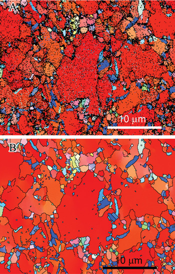
Figure 6: EBSD orientation map of electrodepostied nickel. There are many misindexed and unindexed pixels due to surface preparation and the fine grain size. A) Raw data with only 73% of the pixels correctly indexed. B) Same data as shown in A but noise filtered until all misindexed and unindexed pixels have been removed. This pixel filling used a 4-neighbor rule, iterated until filled.
Problem 2: Systematically Misindexed Pixels
Another rather common problem with EBSD data results from what some analysts have called pseudo-symmetry that results from certain crystallographic orientations not differing much in EBSD pattern symmetry from other orientations. A classic example of this problem occurs when one looks into a face centered cubic (fcc) crystal in the ⟨111⟩ orientation. In Figure 7 two projections of the fcc crystal lattice are shown along the ⟨111⟩ direction. The projection on the left is rotated 60º from the projection on the right. Note the similarity of the two images. Close inspection is required to see the differences. This is the same sort of situation that happens during EBSD map acquisition. Often, if poor acquisition conditions are used, grains or regions of ⟨111⟩ oriented fcc crystals will show a checkerboard-like appearance. This checkerboard is a result of the EBSD software not being able to consistently determine the orientation of the crystal because of this pseudo-symmetry.

Figure 7: Face centered cubic crystal lattices projected along the ⟨111⟩ directions. The projection on the left is rotated 60º about the ⟨111⟩ axis with respect to the projection on the right. Note the similarity of the atomic projections.
The fcc structure is not the only structure that has these problems. Other structures, particularly oxides and inter-metallics, can have unit cells that are only slightly distorted from other crystal structures and that are low in symmetry. Prior et al. [Reference Prior, Mariani, Wheeler and Schwartz4] have pointed out these difficulties and the caution required in filtering the data for geologic materials. These crystal structures give rise to problems similar to those shown for the fcc lattice pseudo-symmetry problems. Another example is bismuth titanate, which is orthorhombic with lattice parameters of a = 0.545 nm (5.45Å), b = 0.541 nm (5.41Å), and c = 3.283 nm (32.83Å) (Figure 8). The a and b cell parameters differ by only 0.004 nm. An orientation map obtained from this material using standard, but inappropriate, acquisition conditions (limited frame integration, 4 × 4 camera binning, normal resolution Hough transform) yields a map as is shown in Figure 9A. Note the many grains with a checkerboard or speckle pattern. This checkerboard is a result of the indexing software not being able to reliably tell the difference between the a and b cell directions for the unit cell. There are also many unindexed pixels (black), particularly at grain boundaries.

Figure 8: Crystallography of bismuth titanate (Bi4Ti3O12, a = 0.541 nm, b = 0.545 nm, c = 3.284 nm). Note that the symmetry down the c-axis, ⟨001⟩, with a nearly equal b, causes the crystal to appear nearly tetragonal.

Figure 9: Inverse pole figure maps (with respect to z-direction) showing the changes in the data for bismuth titanate during noise filtering: A) raw data, B) data filtered for wild spikes and unindexed pixels, and C) data filtered for 90° rotation about ⟨001⟩.
The noise in this data set can be filtered using the procedures discussed above combined with rules for systematic misindexing. The first two procedures for noise filtering discussed above were applied to the data in Figure 9B. In this case, an iterative fill with a 6-neighbor rule was used. These procedures did interpolate most of the unindexed pixels, particularly at grain boundaries, but some unindexed pixels still remain. This procedure did not correct the checkerboard due to the pseudo-symmetry. By telling the software to remove any grain boundaries that are close to 90° about ⟨001⟩, we arrive at the filtered result shown in Figure 9C. Not only does the filter remove the questionable pixels from the orientation map, it also necessarily removes data from the pole figures, thus changing the orientation distribution of the data [Reference Wright, Nowell and Bingert5]. Although this filtered map is more visually appealing and more readily analyzed for grain size, it is potentially inaccurate. There is actually a type of ferroelectric domain boundary in bismuth titanate that is a 90° rotation about ⟨001⟩ [Reference Cummins and Cross6], so when this misorientation is observed in EBSD data, we have confusion about whether the indexing algorithm is being fooled by the pseudo-tetragonal symmetry or whether it is really detecting a domain boundary. At the very least, the analyst should show measured maps with checkerboard patterns and then the same data with the 90°/⟨001⟩ boundaries removed. The best way to solve this problem is to avoid misindexing due to pseudo-symmetry by carefully choosing the EBSD acquisition conditions. When better acquisition conditions (slow acquisition with substantial frame integration, 2 × 2 binning, high-resolution Hough transform) are employed, reliable indexing of EBSD patterns from bismuth titanate is possible as shown in Figure 10. Note that the domain structure is now clearly visible in an orientation map with no cleaning or filtering of the data.

Figure 10: Inverse pole figure maps (with respect to z-direction) of bismuth titanate. This map of raw, unfiltered data was obtained using conditions suitable for a material with unit cell axes that are close in value. Note that very little checkerboard is apparent and that the domain structure is clearly visible.
Conclusion
It is not advisable to apply routines that alter carefully collected experimental data just to make the data or orientation maps more pleasing to the eye. Data cleaning or filtering routines on maps should be used with due regard for data integrity. There are legitimate reasons to filter the noise in orientation maps. For example, it may be of interest to understand the grain boundary character in a sample. In this case, gaps in the data at grain boundaries must be removed in order to extract the information of interest. However, it is good practice to carefully view the raw data before applying secondary processing algorithms. When in doubt, less processing will generally be better than more. At the very least, the analyst should report the noise filter or cleaning procedures used. It is good practice to show the original, raw data whenever possible. With this caution in mind, steps should be taken to ensure that EBSD orientation maps have a high fraction of correctly indexed pixels with a minimum of misindexed or unindexed pixels as-acquired, rather than relying on the various data cleaning routines available for EBSD data.
Acknowledgements
Sandia is a multiprogram laboratory operated by Sandia Corporation, a Lockheed Martin Company, for the United States Department of Energy's National Nuclear Security Administration under contract DE-AC04-94AL85000.


