I. INTRODUCTION
It has been 15 years since the electronic product code (EPC) was first defined by MIT Auto-ID Centre (published 2001) as an innovative replacement for the traditional barcode (UPC). UCC-12 and EAN-13, which are commonly referred to as 1-D barcodes, were arguably the most successful standards ever developed for item-level tracking over the past 40 years. Limited capability and constrained requirements of the UPC has opened the way to the making of Radio Frequency Identification (RFID) technology a more popular and promising substitute in the area of product identification and tracking systems [Reference Brock1]. An authoritative comparison of the two technologies can be found in [Reference White2] but as mentioned in the literature, data capacity is highlighted as the major limiting problem of 1-D barcodes. Although a two-dimensional (2-D) barcoding system allows for increased data housing, compared with their traditional 1-D peers, inherent disadvantages of barcode technology such as line-of-sight, very short range, and slow rate reading capability as well as inefficient operation in harsh and dirty environments highlights the need and demand of a new auto-identification and tracking technology. RFID readers, being one such alternate candidate, use radio frequency communication instead of the optical interface in laser-scanning devices, and as such they are able to read product information from as far away as a few feet or yards. Moreover, electromagnetic (EM) waves can propagate through many material obstacles such as plastic, wood, etc. and thus the RF tags could be read, even when they are rendered invisible to the reader [Reference Xiao3].
A) RFID technology
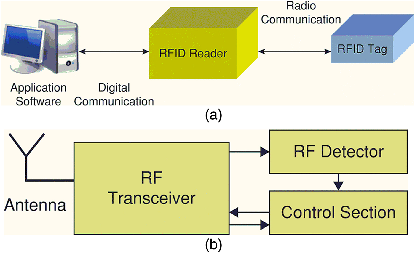
RFID is a contactless data communication technique between an RFID tag, which acts as the data container, and an interrogator device, which is known as the RFID reader. The block diagram of an RFID system is shown in Fig. 1(a). In this technology the reader sends data to the tag using RF waves and in return receives a modulated echo simulating the information stored in the tag, which is then analyzed using a real-time processing system for authentication, detection, and tracking purposes.

Fig. 1. (a) RFID system block diagram [Reference Preradovic, Karmakar and Balbin4], (b) passive RFID tag block diagram [Reference Preradovic, Karmakar and Balbin4].
Many types of RFID tags exist, but for the purposes of general classification, we categorize RFID transponders into three classes: active, semi-active, and passive. Active RFID transponders require a built-in power source; they are either connected to a permanent powered infrastructure or use an integrated battery to supply the required power to the tag. In this case, with active tags there is no requirement of using the carrier signal's energy to energize the data processing and transceiver sections and hence a longer reading range can be achieved. The downside is that the RFID tag's lifetime is limited to the stored battery energy and is dependent on the number of device read operations. Semi-active transponders have the benefit of an on-board battery supply for the data processing, but this power source is not utilized for purposes of signal amplification. The fundamental trade-off here is that the tag's reading range is limited in exchange of increasing its longevity. Passive tags do not contain any source of power supply and are powered entirely by the EM waves generated from the reader. The passive RFID tag utilizes this energy for both communication and data processing purposes. Furthermore, it should be noted that passive transponders may or may not contain an integrated circuit or memory block [Reference Preradovic, Karmakar and Balbin4]. Though active and semi-active tags have increased data storage and data processing capacity as well as increased reading range, as compared with passive tags, the built-in power source, cost and size of tags renders them only suitable to selective (less cost conscious) trades. The block diagram of a passive RFID tag is shown in Fig. 1(b).
B) Passive RFID
Taking advantage of EM wave properties and the near/far fields concepts of an antenna, one may find two different approaches to transfer power from the reader to the tag: magnetic induction (near-field) and EM wave capturing (far-field). In a near-field passive RFID system, the tag will be powered by a magnetic field generated via a large AC current that reader emits via an output coil. Although, near-field coupling was the first approach in the implementation of passive RFID systems, its primary drawback is the inherently short reading range and slow data rates. Near-field techniques allow the tag to be accessible in the approximate range of c/2πf, where c is the speed of light and f is the operating frequency. Therefore by increasing the frequency, a natural decrease of near-field coupling and the reading range will be observed [Reference Want5]. Additionally, the attributes of magnetic field energy of a dipole, dictate that this will decline by the factor of 1/r 6, where r is the distance between the tag and reader [Reference Chawla and Ha6]. To understand the main downsides of near-field tags we can enumerate the large antenna size and the low bandwidth constraints, which contribute to low data-rate. In far-field passive RFID systems, the tag dipole antenna will capture the EM waves emitted by the reader antenna which will be rectified by a diode and capacitor resulting in the required potential for the electronic part. The far-field concept is suited to frequencies larger than 100 MHz and in using this approach, any reading range limitations will be a function of two primary factors; (1) the EM energy captured by the tag and (2) the RFID reader sensitivity. Because the EM wave is essentially attenuated twice based on the inverse square law, the receiving energy will drop off by the factor of 1/r 4 which is smaller than in the near-field range [Reference Chawla and Ha6]. In addition, by taking advantage of new ultra-low-power semiconductor technologies and commercial receivers (the 900 MHz RFID readers with the link budget of about 100 dB [Reference Ghahremani, Rezaei and Sharif Bakhtiar7]), reading range could extend for as much as few meters against only hundreds of mW power consumption.
C) Chipless RFID
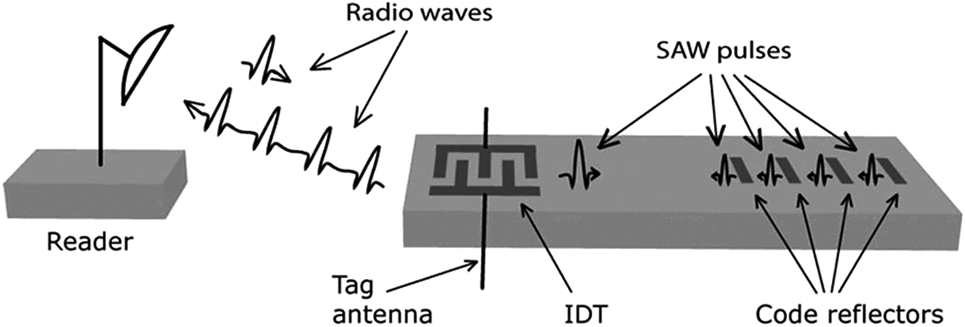
Aside of the obvious merits of integrated circuits (IC)-based RFID tags, as described in our introduction, and further considering the inherent distinction of programmable IC, RFID technology is still not a perfect substitute for the traditional barcode. The need for establishing a very low-cost, robust, and adaptable (able to work in harsh environments) tag as a substitute to traditional barcodes is obvious, therefore it is worth looking at each of these factors and how RFID technology currently stacks up to these demanding expectations and what remedial actions can be taken. The target for achieving a cost competitive RFID tag is less than $0.01, and the best course of action to meeting this target seem to lie in eliminating the electronic chip [Reference Preradovic8]. The current costs of the electronic chip in conventional RFID tags is not the only prohibitive factor in wider scale deployment, the manufacturing process of the composite tag itself is also a costly procedure [Reference Fletcher9]. Cost considerations aside, difficulty in establishing robust connectivity between the IC and antenna when operating in adverse environments seems to be difficult. To address these issues, a new chipless approach has been proposed in recent years. The chipless transponder works on the concept similar to Radar (Fig. 2), where the information is encoded in the EM response of the tag. This response, named EM Signature, is largely dependent on the tags passive physical architecture [Reference Tedjini10]. As the communication principle for a chipless tag is dependent on the backscattered signal from the tag, the performance of the tag could be assessed by the Radar Cross Section (RCS) of the structure. Thus, the antenna RCS optimization and the scattering properties of the tag would be the remaining challenge in the tag design [Reference Penttilä11, Reference Nikitin and Rao12].
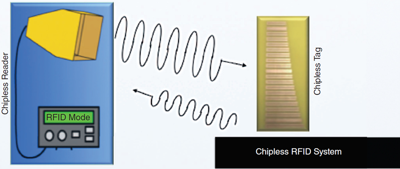
Fig. 2. Chipless RFID System [Reference Tedjini10].
In sync with the above description, the functionality of a chipless RFID tag as a data container on a low-cost substrate is analogous to the optical barcode, though a number of the traditional barcode's disadvantages have been addressed. Chipless tags can be classified based on the information encoding techniques used and can be categorized into two main sub-classes: time domain reflectometry (TDR)-based tags and spectral signature-based tags. However, in recent works two different types of chipless RFID as harmonic and SAR-based RFID have been proposed by researchers. In TDR-based system [Reference Hartmann13–Reference Nair, Perret and Tedjini17], the reader sends a pulse signal to the tag and then listens to the backward echoes of the pulse from the tag while the reflected pulse train demonstrates the encoding information. Much of the work presented in this paper focus on this category of encoding technique. Frequency-domain tags [Reference Jalaly and Robertson18–Reference Vena, Perret and Tedjini21] encode data in the amplitude/phase of the frequency response of the resonant structure. Each data bit is usually associated with the presence or absence of a resonant peak or specific phase at a predetermined frequency in the spectrum [Reference Preradovic8]. In harmonic tag, the reader transmits a signal at frequency f 0 which is received by the receiving section of the tag; then the tag doubles the frequency of this signal to 2f 0 by means of a non-linear device (for example a diode) and sends it back to the reader. Thus, the harmonic is generated and detected by the reader, only in presence of the tag [Reference Virili22, Reference Virili23]. In a more recent approach, an image-based RFID tag surface is illuminated by an EM signal and the reflected signal with orthogonal polarization is collected to generate the EM image of the tag. In this technique, presence or absence of each polarizer in the image represents 1-bit of encoding data [Reference Zomorrodi, Karmakar and Bansal24, Reference Zomorrodi and Karmakar25].
Sensing capability as another prominent advantage of chipless tags in comparison with optical barcodes is also considered within this article. Chipless sensors also have the main profits of chipless tags such as being low-cost and maintenance-free. Any change in sensing parameters results in variation of the tags fundamental properties i.e. permeability, conductivity, and permittivity and these changes are reflected back as amplitude/phase alternations of the backscattered signal [Reference Yang26–Reference Alimenti and Roselli31]. In general, the working principle of the chipless wireless sensors is often the same as those of the chipless RFID tags. By way of example, the sensing parameter is detected by measuring the respective resonance frequency or group delay that is the same as tag detection. Similarly, the pros and cons of both parts of the chipless RFID ecosystem are similar [Reference Mandel32]. In summary the data encoding and detection techniques for chipless sensors are similar to those for chipless tags, and to this effect a review of time-domain based chipless sensors is also considered within this paper.
While frequency-based RFID systems and TDR-based RFID systems both have their own advantages and disadvantages, there is numerous research work on the former and lack of solid work on the later. In continue TDR-based RFID systems will be discussed and prominent achievements in the area will be presented.
II. TIME-DOMAIN TECHNIQUES
A) Surface acoustic wave (SAW)
It has been about 40 years since SAW technology was first introduced as a wireless identification system [Reference Davies, Withers and Claydon33]. However, it has only been in recent years that this technology has seen substantive inroads into a variety of applications ranging from authentication, identification, and localization [Reference Bechteler and Yenigun34–Reference Bulst, Fischerauer and Reindl39]. Indeed SAW tags are the only chipless passive RFID tags that have seen tangible commercialization to date. Using a single-metal-layer photolithographic technology, SAW tags are routinely fabricated in the 2.4 GHz ISM band [Reference Plessky and Reindl40].
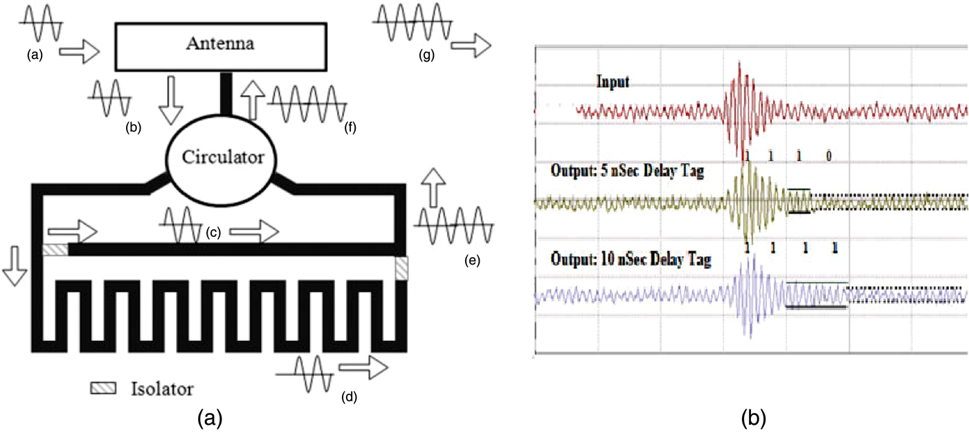
SAW devices work on the principles of piezoelectricity, which essentially means that when applying mechanical stress to certain dielectric crystals, an electrical polarization is generated and contrariwise by applying an electrical field to such a crystal, then mechanical distortions will occur. Using this property of SAW devices leads to producing mechanical output from electrical input and vice versa. This operating principle of a SAW tag is shown in Fig. 3. The tag antenna receives the EM wave emitted by the reader, and then a transduction between the interrogated pulse and 100 000 times slower acoustic wave is achieved by interdigital transducer (IDT). The SAW pulse propagates along the surface of the piezoelectric material substrate such as lithium niobate (LiNbO3) and is reflected partially by each of the metal-based reflectors. In the final stage, the train of reflected SAW pulses are reconverted into an electrical signal by the IDT and retransmitted through the tag antenna [Reference Härmä41]. Since a SAW tag contributes a lot of delay time in backscattered signal, all environmental echoes were sufficiently dissipated when the data signal returned back to the reader so as to be negligible and the data can be analyzed without interference [Reference Reindl42]. The backscattered signal is then utilized by the reader to detect the encoding data.

Fig. 3. Operation principle of a SAW tag [Reference Plessky and Reindl40].
SAW ID tags can be classified based on their geometries. Early version SAW tags of the 1970s included one input IDT and several output IDTs which were connected together electrically (Fig. 4(a)). In this architecture, output transducers worked as reflectors and transducers simultaneously. This resulted in production of counterfeit pulses when an acoustic wave was reflected or generated by a transducer and captured by another transducer [Reference Epstein43–Reference Hartmann45]. To improve this geometry, the encoding output transducers were replaced by reflectors (Fig. 4(b)). In this architecture, the waves go through the reflector and come back to the IDT again for converting to EM pulses [Reference Reindl38, Reference Reindl and Ruile46–Reference Reindl49]. Although this technique allowed for more efficient utilization of the substrate, it still had an inherent loss of 3 dB in IDT for both transmitting and receiving of acoustic waves due to the bidirectional structure of tags. To solve this issue, unidirectional transducers were introduced, where all the reflectors were placed in one side of the IDT (Fig. 4(c)). Work relating to design and implementation of unidirectional transducers which have been reported in literature [Reference Holland48, Reference Lewis50–Reference Wright, Thompson and Chang53] seek to address two strategic goals: increasing bandwidth and reducing tag size. To make SAW tags more suitable for commercial usage, the number of encoding bits should increase proportionally to size. Based on Shannon's theory [Reference Shannon54], the number of encoding bits is specified by the multiplication of bandwidth and coding delay time. Due to size limitations and also high propagation losses in the GHz frequency range the delay time should not be more than the order of few microseconds. Therefore to achieve the required encoding capacity of 96 bits for EPC, a bandwidth in the order of tens of MHz is required. This could be theoretically applicable in the 2.45 GHz ISM band, however currently this frequency band is utilized by a tremendous amount of short-range communication applications.

Fig. 4. SAW tags [Reference Härmä41]: (a) transducer-based tag, (b) reflector-based tag, and (c) unidirectional tag.
There are many encoding techniques reported for SAW RFID tags in the literature. Most of the SAW tags utilize time position encoding which is illustrated in Fig. 5 [Reference Epstein43, Reference Plessky47, Reference Reindl49, Reference Stelzer55]. In these tags a synchronizer reflector is used to identify the initial point for the train of pulses. As the velocity of EM waves is about 300 m/µs, in most cases there would be at least 1 µs time gap between the reader interrogation signal and the start pulse, in order to allow the reader to be able to distinguish between the real reflection from the tag and fake reflections from the other environment obstacles. A single reflector placed in each data group contains n pulse positions. Also, an embedded distance for the separation of two data blocks is specified. By using m reflectors, the data capacity of tag will be identified by m × log2 n bits. Since the number of pulses for each tag remains fixed (only one pulse per each data block and total of m pulses for tag) the uniform amplitude of responses could be provided by adjusting the strength of the reflectors appropriately. Maybe the simplest encoding method is on/off pulse keying in which the presence or absence of each pulse in a predetermined position is considered as a single bit [Reference Cole and Vaughan44, Reference Reindl and Ruile46]. Although there is no gap between two consecutive positions, to save tag space, the width of pulse slots should be increased to achieve enough separation between adjacent pulses. Phase modulation is another scheme of data encoding implementation. By exact phase measurement of reflected pulses, the data capacity of the tag will increase considerably. As the reflector electrode width is much smaller than the required space for a slot, by locating the reflector in an accurate position, the phase of the received pulse could be considered as an extra encoding parameter. Studies with four and eight phase steps were reported in the literature [Reference Harma52, Reference Tavakoli56, Reference Kuypers57]. The orthogonal frequency coding (OFC) method was developed by Malocha et al. [Reference Malocha, Puccio and Gallagher58–Reference Puccio60]. The key characteristic of OFC SAW implementation is a precise design of the reflectors in a manner that the orthogonality conditions are fulfilled. In the frequency orthogonality condition, one reflector peak frequency response is at the null of all other reflectors responses. In this case, while each reflector seems to be transparent to the other reflectors, strong reflectivity is permitted and hence the total loss will decrease.

Fig. 5. Time position encoding in SAW tags [Reference Stelzer55].
In literature, the Hartman Global SAW ID Tag [Reference Hartmann13, Reference Hartmann, Brown and Bellamy61, Reference Hartmann62] has been introduced as a breakthrough in defining a SAW tag with capability of infinite coding capacity. The encoding scheme in the proposed tag was Time Overlapped Pulse Position with simultaneous Phase offset modulation (TOPPS). It has the advantage of many more pulse time positions being allowed due to the fact that the time steps are much smaller than the pulse width (Fig. 6). In this tag, pulse overlap is allowed under the Nyquist condition which means between each two pulses the minimum spacing has to be considered in such a way that each pulse does not distort the peak phase of the neighboring pulse. Similarly, Plessky and Reindl in 2010 introduced the best geometry for a SAW tag based on a unidirectional transducer (SPUDT) and loss compensable reflectors [Reference Plessky and Reindl40].

Fig. 6. Global SAW tag data encoding [Reference Hartmann13].
The possibility of using ultra-wideband (UWB) signals for SAW ID tags has been considered by the authors [Reference Malocha63–Reference Pohl65]. As the frequency bandwidth is one of the key parameters in identifying the coding capacity according to Shannon's equation [Reference Shannon54], increasing the bandwidth leads to time decrease. For example, a bandwidth of 400 MHz in UWB technology instead of 80 MHz in 2.45 GHz ISM band will reduce the coding duration to hundreds of ns instead of few μs [Reference Lamothe66]. Additionally, by designing a chirp transducer it is possible to compress the incoming pulse and retransmit it in the time-reverse situation of the interrogation signal. Thus, the tag reflection is different from other environmental echoes and could be detected easily with a match filter signal processing technique in the reader [Reference Harma67].
In spite of high propagation delay, piezoelectric materials suffer from temperature and mechanical force sensitivity and also high losses due to conversion and reconversion of EM waves to acoustic waves. The requirement of using the extremely busy 2.45 GHz ISM band for communication is another disadvantage of SAW-based identification (ID) tags.
SAW devices also can be used as sensors for measurement of physical or chemical parameters if they are able to either alter the velocity of the acoustic wave or deform the mechanical structure of the SAW chip [Reference Reindl68]. In sensor applications one needs to measure the time from transmitted interrogating signal to the backscattered response and to measure the time between two or more reflected signals, respectively. The first measurement contains information about the relative distance between the interrogator antenna and ID tag. The second gives us the propagation time of the acoustic wave on the substrate. This time depends on the distance between reflectors and how the sound velocity is influenced by different physical conditions [Reference Schmidt69]. Table 1 shows the effect of different physical parameters on SAW substrate materials [Reference Pohl70]. For example, temperature changes the velocity of acoustic waves directly and it was reported upon extensively by authors [Reference Reindl49, Reference Pohl65, Reference Bao71–Reference Kang73]. But for measuring mechanical parameters like pressure [Reference Sinha74, Reference Scherr75], strain [Reference Sallee76] or acceleration a suitable mounting and packaging is required. Other parameters such as gas detection [Reference Venema77], humidity [Reference Caliendo78], voltage [Reference Gatti, Palma and Verona79] or magnetic fields [Reference Reindl38] can be measured by coating the SAW tag with a specific material.
Table 1. Linear coefficients for physical effects on SAW substrate materials [Reference Pohl70].

B) On-off keying (OOK) modulation
Maybe OOK is considered as the simplest method of data encoding in TDR-based chipless RFID systems. In this case, the presence of a signal in a predetermined duration of time represents logic 1, while its absence is considered as logic 0.
In 2006, L. Zhang et al. reported the first time-domain chipless RFID utilizing this technique [Reference Zhang80]. The reader sent a short-time pulse and the reflections due to capacitive impedance mismatches at certain intervals in the tag were transmitted back to the reader. The schematic of the tag is shown in Fig. 7. The total length of transmission line was determined by two parameters: encoding capacity and interrogation signal pulse width. By altering the capacitance values at each discontinuity spot, the reflection coefficient was adjusted in such a way that the amplitudes of the reflected signals would be equal. Additionally, a matching resistor was placed at the end of the line to absorb any redundant energy. A 4-bit tag using a meandered transmission line on a Rogers 4350 substrate (ε r = 3.48, H = 0.25 mm) with a Gaussian pulse of 2 ns width was realized. For each bit a transmission line segment of 180 mm was required (Fig. 8(a)). To design a printable tag, the authors replaced the SMT capacitive discontinuities with passive radial planar capacitors in an 8-bit tag [Reference Zheng15]. To reduce the tag size with the same substrate, an interrogation pulse width of 0.4 ns was selected. Therefore the total transmission line length would be 400 mm for an 8-bit tag (Fig. 8(b)). Unfortunately to avoid the reinforcement of interference ringing caused by three or more consecutive capacitances, the encoding capacity decreased from (28 = 256) to (34 = 81). Another enhancement was achieved by replacing the substrate with paper to achieve a fully printable chipless tag [Reference Shao81]. To generate a 3.6 ns time interval on Epson glossy photo paper (ε r = 2.8, H = 280 µm) [Reference Shao82] with a backside silver coated ground plane, the length of each segment of transmission line should be 65 mm. To compensate the mismatch effects of printing silver on paper compared with conventional copper on PCB, uniform microstrip line was replaced by Tapered Microstrip Line (TML) because of the difference in the characteristic impedances and series resistances of the transmission lines. TML is defined as a microstrip line with its signal track width varying slightly. For a 4-bit tag, TML width ranged between 719 and 1678 µm. TML tag prototype, measured results and system block diagram are shown in Fig. 9.
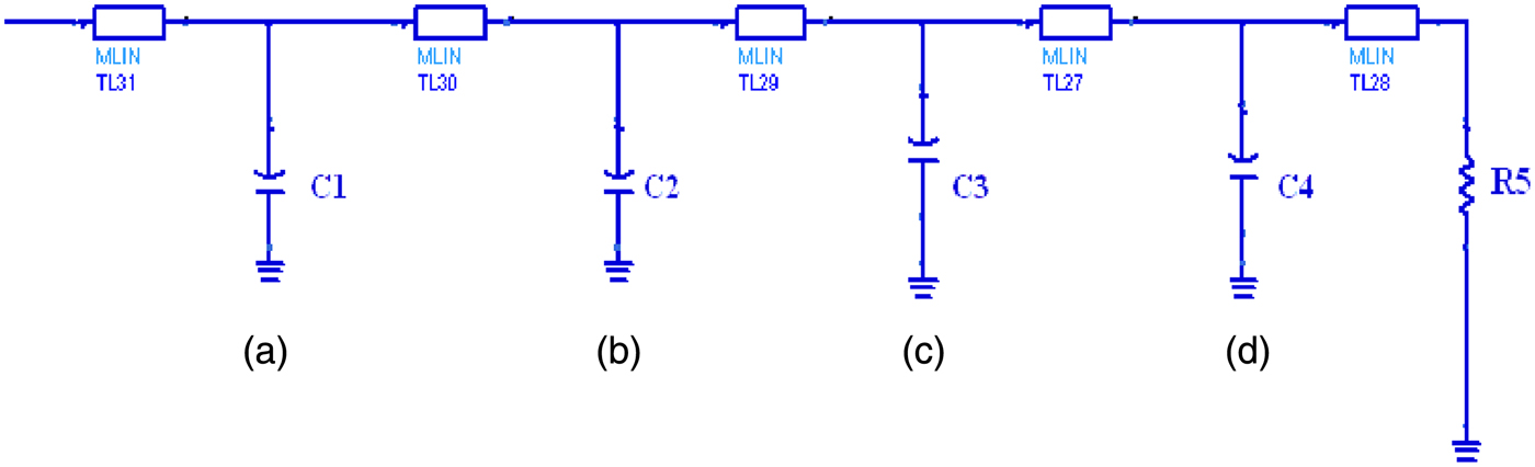
Fig. 7. Schematic of proposed tag in [Reference Zhang80].
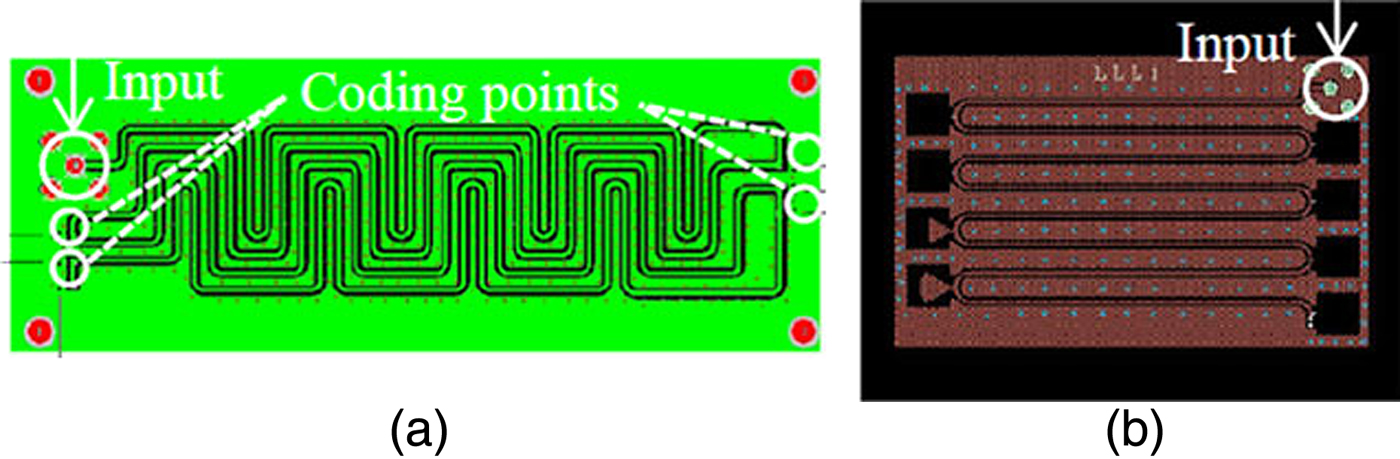
Fig. 8. Delay line proposed in [Reference Shao127]: (a) circuit layout for 4-bit coding, (b) circuit layout for 8-bit coding.
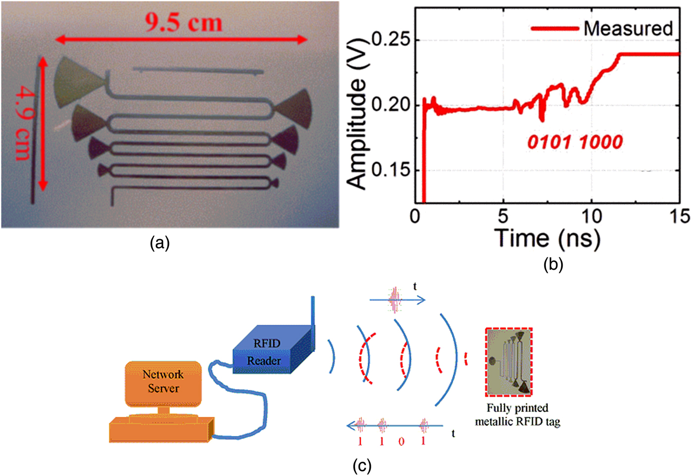
Fig. 9. Prototype tag proposed in [Reference Shao81]: (a) layout, (b) Measured result using TML, and (c) whole system schematic [Reference Shao127].
In another approach a 4-bit ID generation circuit operating on a flexible substrate FR9151 with a reading range of 10 inches, shown in Fig. 10(a), was reported in [Reference Chamarti and Varahramyan14]. It contained an omnidirectional triangular patch antenna with a center-resonant frequency of 915 MHz [Reference Vemagiri83] and two transmission line branches, one short and straight and the other meandered to generate different delayed versions of the interrogated signal. Using isolators the signal in the meandered branch could be tapped at time delays equal to the discrete multiples of the width of the input signal. The tapped signals with different time delays were superimposed on to the straight branch to produce the output signal. The choice of discrete lumped components (circulator MAFRIN0497) makes the achievement of a low-cost tag challenging. Rather than a single antenna having a circulator to control when the antenna was in transmitting or receiving mode, an additional receiving antenna had the advantage of not requiring a circulator, but conversely the disadvantage of requiring addition substrate space to accommodate two antennas [Reference Varahramyan84]. The tapping RF isolators CES40925MECB000RAB were costly for a chipless RFID and the propagation of the signal through long transmission lines contributed to high insertion losses for higher order data bits (Fig. 10(b)).

Fig. 10. RFID tag proposed in [Reference Vemagiri83]: (a) schematic, (b) measured input and output waveforms of the ID circuit.
C) Pulse position modulation (PPM)
In PPM an n-bit encoding could be provided by dividing each time slot into 2 n possible pulse positions with a single pulse. By locating one reflector in each time slot, one and only one pulse will be reflected back to the interrogator. One of the key features in this method is to synchronize the reader to detect the pulse position of the tag response. For example in SAW tags, one starting reflector could be used as a synchronizer for this purpose. In chipless RFID tags, the backscattering modes produced by the tag antenna are considered for this synchronization. The reflected signal from the tag has two modes: first, Structural Mode: which is due to currents induced on the antenna's surface when it is terminated with the complex-conjugate impedance and second, Antenna Mode: which is due to the mismatch between the antenna impedance and the tag impedance [Reference Nikitin and Rao12]. Because the Structural Mode is constant for all tags, it can be used as reference for time synchronization, therefore the time difference between these two modes can be utilized for encoding.
Most of the work reported in this category used only one time slot for encoding. Reflection pulses with different positions related to the Structural Mode pulse were generated by connecting the antenna to a varying length transmission line ended with a mismatched load. In [Reference Hu85, Reference Hu, Law and Dou86] S. Hu et al. proposed a tag with a trimmed elliptical ring path as the radiation element fed with a coplanar waveguide (CPW) transmission line on a substrate of Rogers RO4003C (ε r = 3.38, H = 0.508 mm) with a size of 23 × 23 mm2. An interrogation pulse of 0.35 ns at a center frequency of 7.5 GHz was examined while the distance between the interrogator and tag was 0.8 m. Transmission lines with two different lengths of 37.6 and 41.7 mm were fabricated to generate 519 and 561 ps delay times, respectively (Fig. 11). As a transmission line, CPW seems to be more suitable compared with Microstrip since it does not need via for short termination. Three different terminations of match, short, and open were chosen to improve coding with a higher order phase modulation. To improve the Antenna Mode response of the tag, an interrogation pulse with a center frequency of 4.1 GHz helped to reduce the propagation loss, however increasing the pulse width to 1 ns led to pulse overlapping [Reference Shen87]. A new signal processing method based on a calibration setup was proposed to detect the overlapped Structural and Antenna Mode pulses; hence the transmission line length could be reduced. For greater enhancement, a circularly-polarized antenna which is shown in Fig. 12 was used instead of a linearly polarized one in previous works [Reference Shen and Law88, Reference Shen, Law and Shen89]. It increased the tag size slightly but had the advantage of significant reduction of the coupling between the transmitter and receiver antennas.
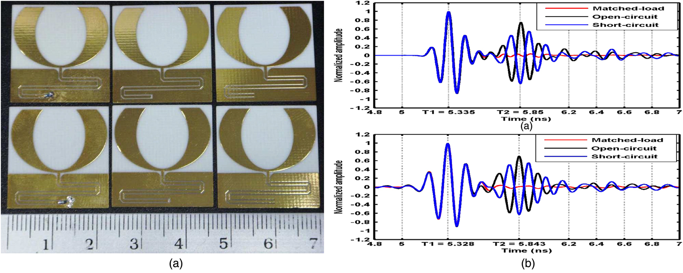
Fig. 11. RFID tags proposed in [Reference Hu85]: (a) layout, (b) measured backscattered pulses using 7.5 GHz transmitter.
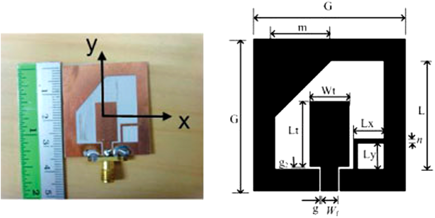
Fig. 12. Prototype and geometry of the UWB circular polarized antenna proposed in [Reference Shen, Law and Shen89].
In a similar approach [Reference Ramos16], an eccentric annular monopole UWB antenna was connected to several coaxial lines of different lengths to generate reflection pulses with different delays. The antenna was fabricated on Rogers 4003 (ε r = 3.38, H = 32 mil) with a total size of 57 × 70 mm2 (Fig. 13). A commercial radar including a signal generator (GZ1120ME-50EV) and sampler with triggering capability (GZ6E) performed the data generation and collection instead of a vector network analyser (VNA) and digital signal oscilloscope (DSO). Measurements with seven different coaxial lines ranging from 252 to 568 mm were studied. To improve the detection in noisy environments and also to increase the reading range, signal processing methods including background subtraction, time gating, and continuous wavelet transform in the reader side were developed [Reference Lazaro90]. Another commercial measurement setup (Novelda radar) was used to examine three different tag structures to show the fact that relation between Antenna Mode and Structural Mode increases by reducing tag dimensions and specifically the metallic area; hence this led to a larger reading range of 2 m [Reference Girbau, Lázaro and Ramos91].
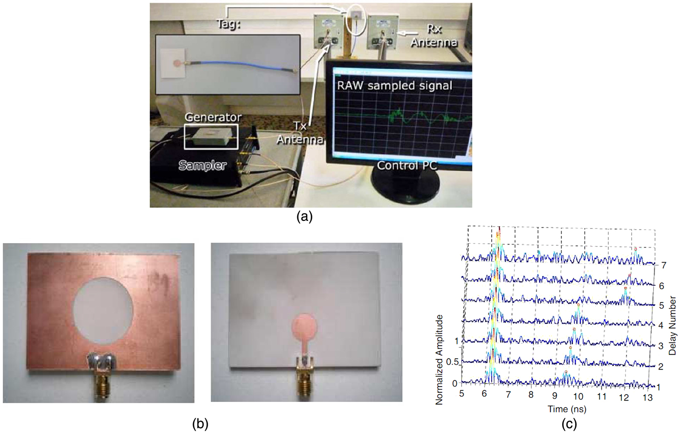
Fig. 13. Tag proposed in [Reference Ramos16, Reference Lazaro90]: (a) photograph of experimental setup based on UWB-IR, (b) photograph of antenna, and (c) measured results with different transmission line lengths.
D) Metamaterial structures
The maximum number of bits in the delay-line-based backscatter tags (n bits ) is limited by the number of pulses that can be stored on the line. Given a single pulse line length (L pulse ), to increase n bits for a certain length of transmission line, L pulse should decrease. While L pulse depends on the product of the group velocity vg and the pulse duration τ, in order to increase n bits the group velocity has to be minimized [Reference Schuler92]. In general “Metamaterials” refer to structures whose behavior, due to their artificial nature, can be engineered in such a way that they show a relative permittivity and/or permeability with values between −∞ and 1, something which is not possible for “natural” materials. These structures allow us to construct materials with negative refractive indices and phase and group velocities pointing in opposing directions [Reference Mandel32]. There are two main approaches for the implementation of metamaterial transmission lines: (1) the LC-loaded approach, where the host line is loaded with series capacitances and shunt inductances, and (2) the resonant-type approach, where the line is loaded with electrically small resonators, such as Split Ring Resonators (SRRs) or other related resonators, plus additional reactive elements [Reference Mandel32].
In [Reference Schüßler, Damm and Jakoby93] a periodically LC-loaded left-handed transmission line was examined to realize an electrically long but physically short transmission line. Due to the dispersive nature of LH lines, the interrogated pulse is broadened when passing through a large number of cells. A 40-cell LC-loaded delay line with 0603 SMD capacitances and inductances embedded on a 50 Ω CPW line (no via required) on a 1.6 mm FR4 substrate for 3-bit data coding was demonstrated. A total delay of 12 ns with 21 dB loss was achieved. Physically realized left-handed structures always show an additional right-handed behavior caused by parasitics, which is appropriately described by the Composite Right/Left-Handed (CRLH) model. In a complementary work [Reference Schuler92], a same-size 100-cell CRLH coaxial line with a rectangular cross-section connected via an SMA connector to a wideband monopole antenna was designed. In contrast to the previous work all reactive elements were realized on the top and bottom sides of a 50 µm ULTRALAM 9808 substrate, demonstrating a printable inexpensive tag. Each cell length was 1.1 mm and the total coaxial line size was 120 × 14 × 10 mm3 (Fig. 14(a)). A total delay of 25 ns with an overall 20 dB loss for realization of a 4-bit tag was reported. The measurement result is shown in Fig. 14(b); and it is obvious that for complete detection of all data bits at least 20% bandwidth is required. A higher-order phase modulation was contemplated in [Reference Mandel94] to more efficiently usage of the bandwidth. Exploiting only one element (either a capacitor or an inductor) as a reflecting and phase-shifting element at the same time, a Quaternary Phase Shift Keying was realized. The proposed delay line was made of 20 left-handed unit cells with a delay of 5 ns between two neighboring pulses at the carrier frequency 2.2 GHz and 32% bandwidth. It consisted of three line elements and three passive reflectors with four different phase modulators, thus a 5-bit coding was achieved in a 26 cm tag.
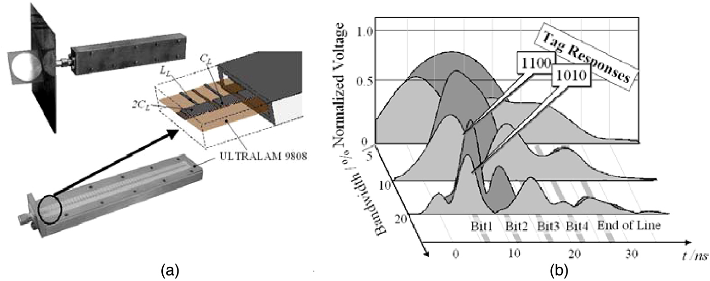
Fig. 14. Tag proposed in [Reference Schuler92]: (a) photo of the tag, (b) measured impulse response of “1100” and “1010”.
In a resonator-based approach, F. J. Herraiz-Martinez et al. proposed a tag composed of a printed antenna, a Microstrip line and a chain of squared split ring resonators (SSRRs) working with the same concept as SAW tags but completely printable on one side of a dielectric substrate [Reference Herraiz-Martinez95]. The chain of SSRRs acted as a delay line which allowed the propagation of magneto-inductive-waves (MIWs). MIWs are slow waves which can propagate along periodic structures where the elements are magnetically coupled [Reference Marqués, Martín and Sorolla96]. A Microstrip line connected to the antenna and inductively coupled to the first SSRR of the array served as the transducer between the Microstrip mode and the MIW mode. Finally, the additional Microstrip lines were coupled between specific pairs of SSRRs and generated partial reflections that were used to implement the digital ID code of the tag. These slow wave structures exhibited group velocities as small as c/100 (instead of c/10 for CRLH), and their main advantage compared with CRLH transmission lines were their narrow bandwidth requirement. The MIW delay lines in this report were designed to work in the 2.45 GHz ISM band on a RO3010 (ε r = 10.2, H = 635 µm) substrate. A 2-bit tag with a total delay of 32 ns was reported (Fig. 15) [Reference Herraiz-Martínez97]. The main limitation of the proposed tag was the high losses of the MIW delay lines that had a significant negative influence on the tag's coding capacity.
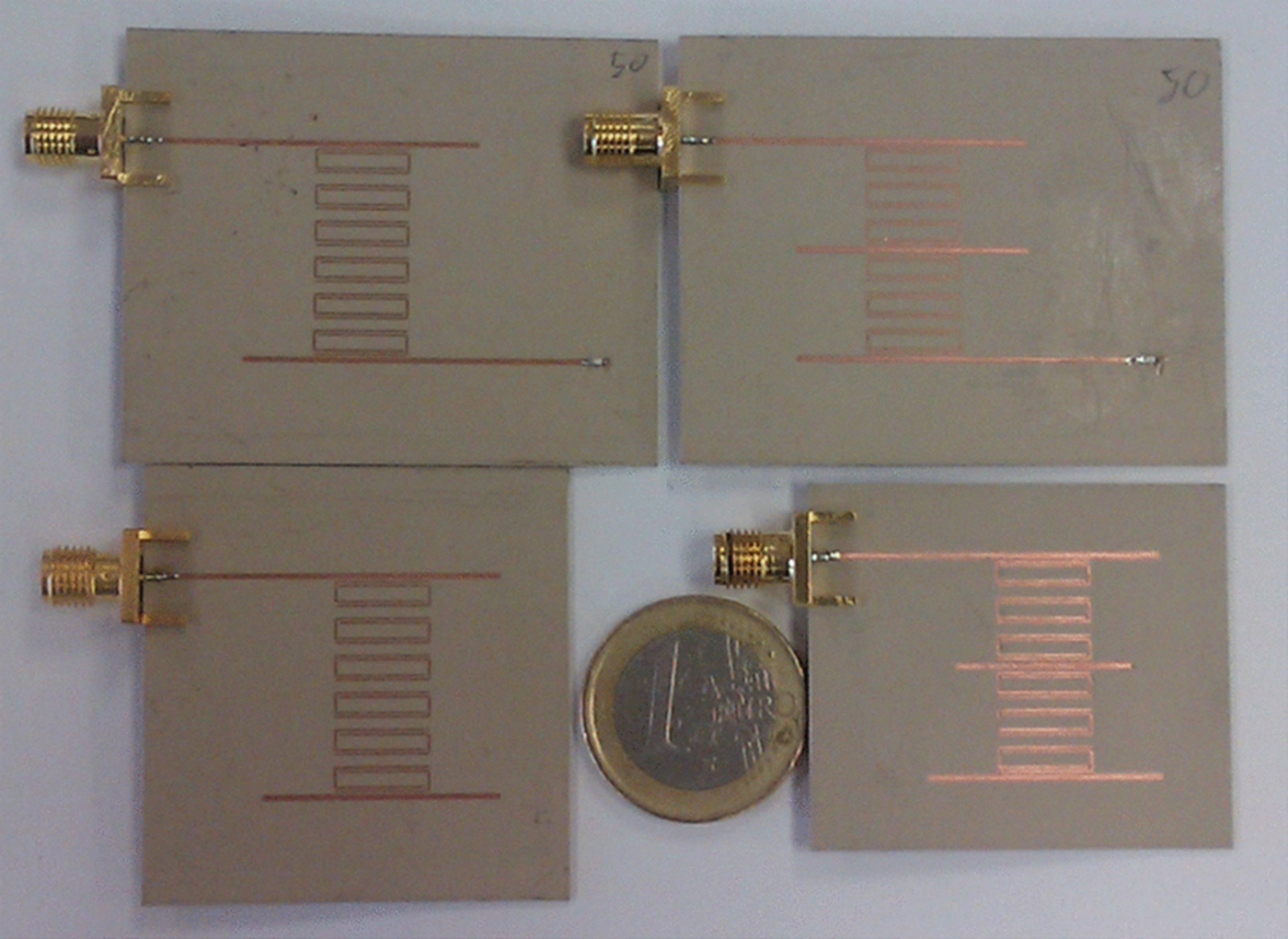
Fig. 15. Photograph of the fabricated set of 2-bit SSRR-based delay line in [Reference Herraiz-Martínez97].
E) Multi-frequency pulse position modulation
All time-domain chipless tags previously described have operated in a single frequency while the generated delay was independent of frequency. So, to increase the coding capacity in the time-domain, designing tags with frequency-related delay lines has been considered in recent years. To this effect, a dispersive transmission line section known as C-sections which are able to produce different group delays at different frequencies has been proposed in the literature. Furthermore, since group delay is calculated by taking the negative derivative of the phase with respect to angular frequency, it is more robust than amplitude coding systems. One of the main differences between this method and the aforementioned methods is that in the current structure instead of one antenna, two orthogonally oriented antennas (one for reception and one for transmission) are used. Although this contributes to larger tag size, the backscattered signal could easily be isolated from the interrogation pulse and environmental reflections.
A C-section is created by shorting one end of a coupled transmission line (Fig. 16), however they use the coupling effect between each transmission line section in contrast to the meandered transmission line [Reference Nair, Perret and Tedjini98] to produce a delay. E.G. Cristal proposed the analytical properties of cascaded commensurate transmission line C-sections in [Reference Cristal99], while Gupta et al. in [Reference Gupta100] presented an ultimate procedure to characterize the group-delay of non-commensurate all-pass C-section networks. The concept of transmission-type all-pass dispersive delay structures (DDSs) for TDR was proposed in [Reference Gupta, Nikfal and Caloz101] for the first time. A 3-bit encoding system operated in 3, 4, 5 GHz frequencies with tags fabricated in Stripline technology on a RO4003C substrate (ε r = 3.55, H = 20 mil) with a CPW-to-Stripline transition and two wideband monopole antennas was reported. As illustrated in Fig. 17, the encoding data were detected successfully however the output signal was significantly distorted.
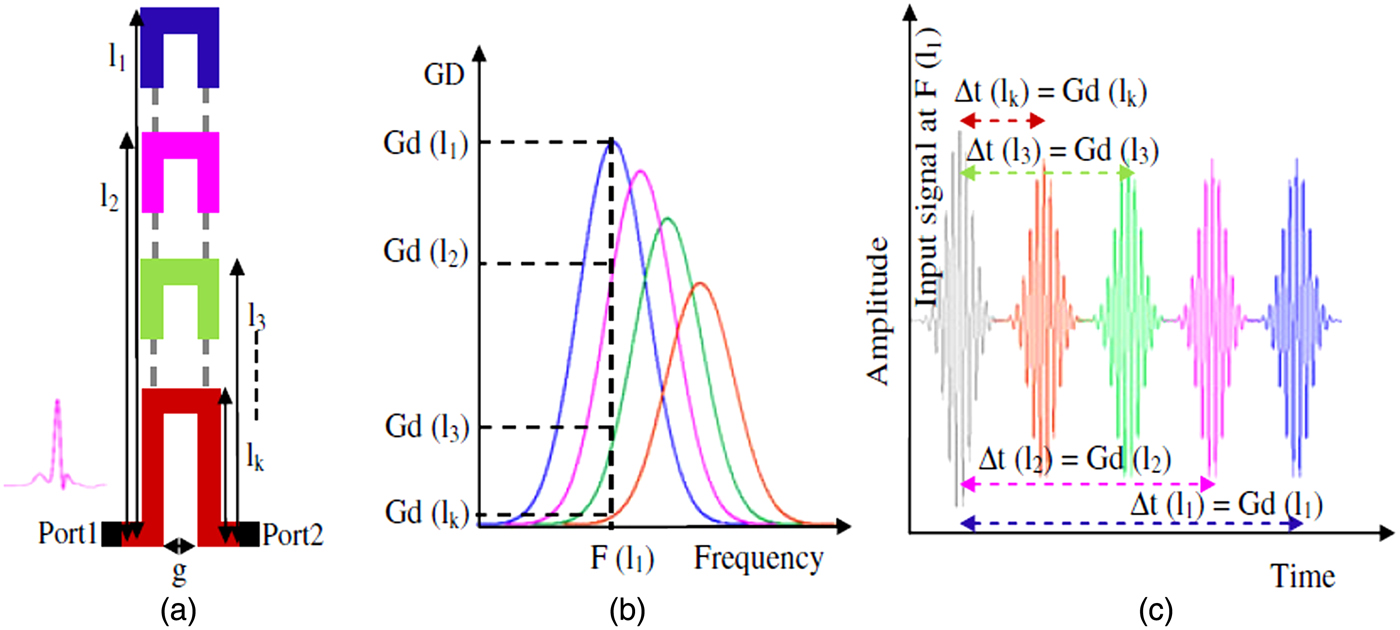
Fig. 16. Principle of encoding for C-sections: (a) design parameters, (b) group delay versus frequency response, and (c) corresponding time domain response. [Reference Nair, Perret and Tedjini98].
Fig. 17. Measured time-domain signals in [Reference Gupta, Nikfal and Caloz128]: (a) PPM coded signals with their envelopes, (b) corresponding extracted codes.
For further development of the idea, R. Nair et al. implemented a 2-bit tag with dimensions of 102 × 48 mm2 and C-sections of two different lengths (17.87 and 8.93 mm) to provide good isolation between each group [Reference Nair, Perret and Tedjini17]. This structure was fabricated on a FR4 substrate in conjunction with two disk monopole UWB antennas. Increasing the length of each section by a small amount of Δl 1 and Δl 2 which were chosen to be 2.98 and 0.81 mm, the group delay related to each frequency increased. In order to reduce the mutual coupling effect between each group of C-sections, the gap between two groups was increased to 1 mm. To produce a distinguishable delay in each frequency, the number of C-sections in each group was increased [Reference Nair, Perret and Tedjini102]. An impulse with 80 ps pulse width was generated with an impulse generator (Picosecond Pulse Labs-Model 3500) for experimental validation of the proposed reading range of 1.2 m [Reference Nair, Perret and Tedjini98]. The time difference between the Structural Mode and Tag Mode was measured with digital oscilloscope (Agilent DSO91204A) for encoding purpose. This time difference would be the sum of the group delays produced by the C-sections and the two antennas [Reference Nair, Perret and Tedjini103]. The results obtained from four tags with multi C-section structures in response to an interrogation pulse with carrier frequency of 2.45 and 5.8 GHz ISM bands are shown in Fig. 18.
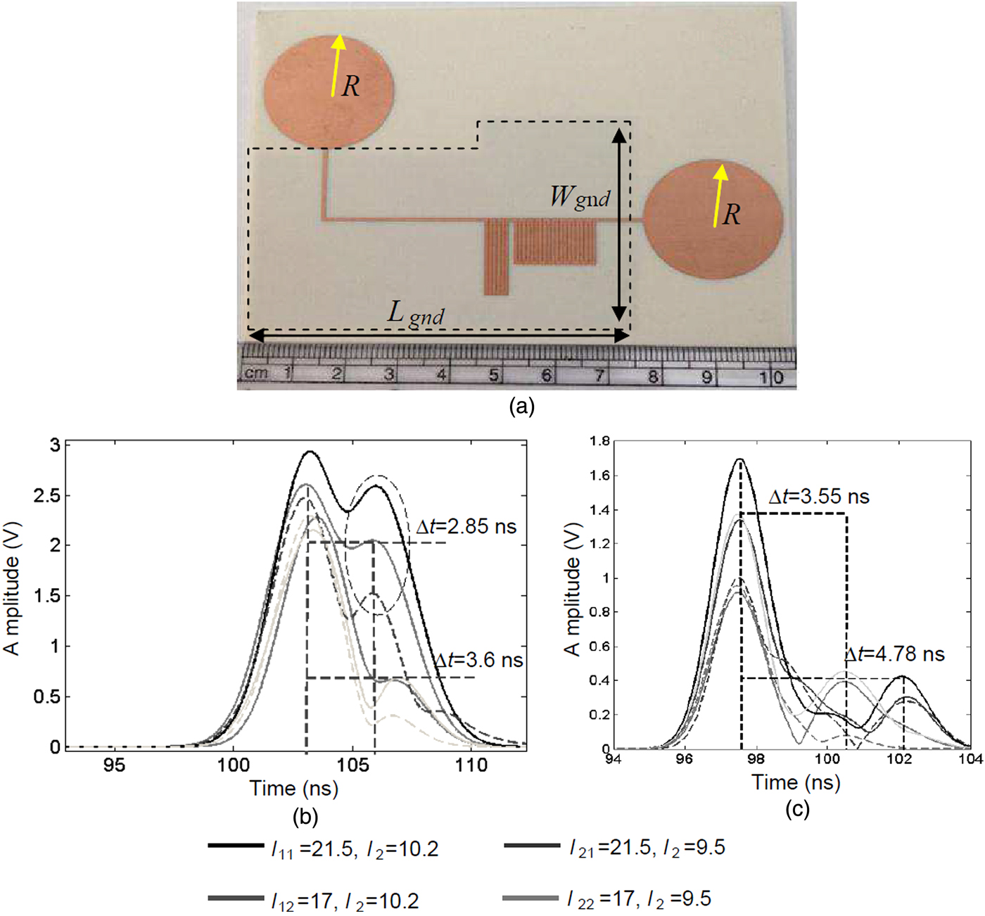
Fig. 18. (a) The proposed chipless tag in [Reference Nair, Perret and Tedjni129] and measured delays for two groups of C-sections at (b) 2.45 GHz, and (c) 5.8 GHz.
III. CHIPLESS SENSOR
Chipless wireless sensing is derived from changing the EM response of the chipless tag by modifying the conductivity, permittivity or permeability of an ID-tag which includes a sensitive material. This modification would nominally present itself as a change in the amplitude level variation or frequency and phase shifting of the transponder. The main difficulty to chipless wireless sensing arises when the reader has to detect the tag ID and sensing parameter simultaneously. To redress this problem two major workarounds have been considered: in the first option the signal characteristic used for encoding would differ from that used for sensing (e.g. pulse position and phase shift). In the second scenario, the encoding and sensing circuit would use the same characteristic of the signal but their dynamic range would be significantly different such that the effect of each part would be distinguishable on the reader end. Most of the aforementioned time-domain techniques which have been implemented for identification are suitable for wireless chipless sensors as well.
A PPM-based RFID sensor system was presented in [Reference Shrestha27] for wireless monitoring of ethylene concentration, which included a meandered Microstrip transmission line for 3-bit ID generation in the 915 MHz ISM band and an integrated sensor as a capacitive load to the transmission line (Fig. 19). The Antenna Mode of the backscattered signal was used for both ID generation and parameter sensing. The relative position of the Antenna Mode signal with respect to the Structural Mode signal could be varied by changing the length of the transmission line and this was utilized for pulse position modulated ID code generation. At the same time changing the capacitive load led to a different Antenna Mode signal phase. An average of 26.51°/pF phase shift in the reflected signal was demonstrated, when the transmission line load capacitance changed between 1 and 5 pF.
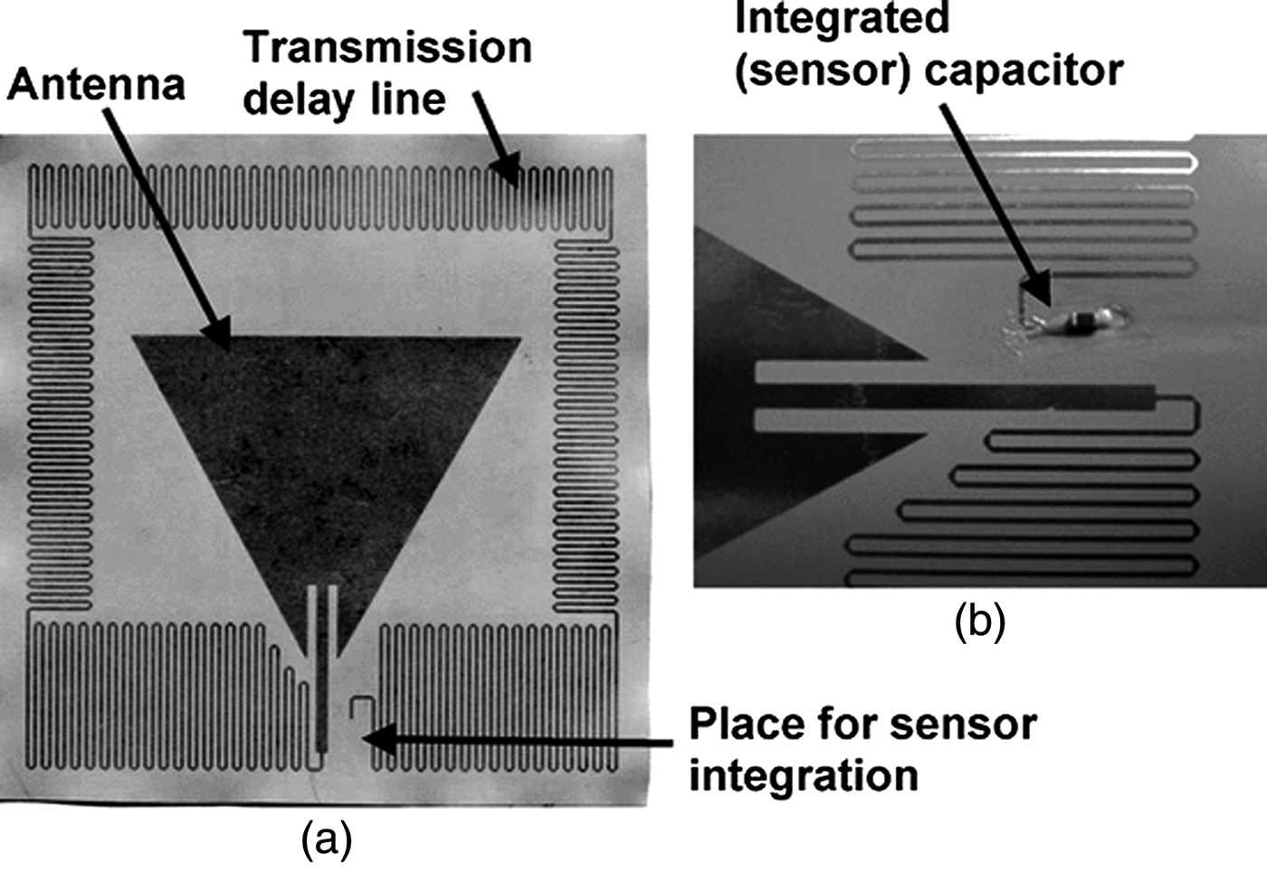
Fig. 19. Proposed ID-enabled SnO2 sensor in [Reference Shrestha27]: (a) prototype tag, (b) integrated sensor (capacitor).
A passive wireless temperature sensor with identification capabilities based on a phase modulation scheme was discussed in [Reference Schuler104]. A 60 cell LH delay line consisting of SMD capacitors and High-Q air-core inductors working at a center frequency of 2.2 GHz and bandwidth of 800 MHz was presented for 3-bit symbol with OOK modulation. While the phase shifting method was considered for temperature sensing, the temperature dependent part of the phase shifter was realized using an interdigital capacitor based on Barium-Strontium-Titanate (BST) thick film technology. Since BST shows an intrinsic permittivity dependence on temperature, the capacitance of the device would be affected as well. The average sensitivity of 0.5°/K in the range of 40–100 °C was achieved since the load capacitance seemed to decrease roughly linearly (Fig. 20).

Fig. 20. Proposed temperature sensor in [Reference Mandel130]: (a) measured phase change of the sensor over temperature, (b) capacity of the sensing BST capacitor over temperature.
Another chipless temperature sensing system was reported by D. Girbau et al. in [Reference Girbau105]. A broadband eccentric annular monopole antenna connected to four different delay lines was considered for a 2-bit ID generation section. The transmission line was loaded with a resistive temperature sensor while the temperature value was modulated in the amplitude of the backscattered signal. To detect temperature in range of 30–130 °C a Vishay PTS series resistor was chosen as the transmission line load. Temperature variation caused load change and hence the backscattered Tag Mode had a different amplitude compared to the Structural Mode.
In [Reference Nair106] a group delay based humidity sensor was proposed for chipless RFID applications. The sensor included one group of C-sections as the ID generation circuit and silicon nanowires deposited on the transmission line as the sensitive material. The tag ID purely depended on the length of the C-section while sensing was achieved by changing the permittivity of the nanowires via humidity absorption, which in turn changed the RCS, phase, and hence group delay of the tag. An RCS change of 30 dB and a group delay variation of nearly 22.3 ns were reported near the fundamental frequency of 3.7 GHz over a bandwidth of 40 MHz for a relative humidity variation of 60.2–88% [Reference Nair107].
IV. TIME-DOMAIN MEASUREMENT
Thus far, much of our discussion has been focused on the RFID tag requirements. However in parallel to the tag design, the design of robust and cheap RFID readers needs to be taken into consideration if the technology is to become more widely commercialized. In time-domain based chipless RFID systems, since an ultra-short pulse is required for tag interrogation (<10 ns) based on bandwidth, an Ultra-Wideband Impulse-Radio (UWB-IR) reader seems to be the most suited to this purpose. Unfortunately, the design of time-domain based RFID readers has not received much attention in the literature [Reference Karmakar108, Reference Xia109]. Most of the authors for generating interrogation impulses and capturing the backscattered signals performed measurements with expensive laboratory equipment such as VNAs, signal generators and DSOs which are not suitable for commercial applications. However, some commercial Impulse Radars have been reported in the literature (Geozondas [Reference Ramos16, Reference Lazaro90, Reference Girbau105], Novelda [Reference Girbau, Lázaro and Ramos91, Reference Nair, Perret and Tedjini98, Reference Ramos110] and PulseON P400 [Reference Ramos, Lazaro and Girbau111, Reference Lazaro112]).
Apart from time-domain systems, spectral signature-based chipless RFID systems ultimately benefit from UWB-IR interrogators as well [Reference Kalansuriya and Karmakar113–Reference Vena118]. A short UWB pulse interrogates the tag and the frequency signature of the tag can be delivered easily using a signal processing method based on the Fast Fourier Transform of the backscattered signal. UWB-IR is much faster than a chirp signal generator since generating an interrogation signal for the chirp signal generator in the operating bandwidth of the tag takes much more time. Furthermore, a high performance wideband Voltage Controlled Oscillator (VCO) with low settling time is an expensive component in Frequency Modulated Continuous Wave-based (FMCW) readers [Reference Koswatta119]. Additionally, to be compatible with Federal Communication Commission (FCC) regulations, generating CW signals over a wide range of spectrum will result in a very low interrogation power and therefore lower reading range of the system as a whole. To overcome this problem, the UWB technique has been chosen in literature for many systems [Reference Vena, Perret and Tedjni120, Reference Dardari and D'Errico121]. In February 2002 the FCC gave permission for the use of a power spectral density of −41.3 dBm/MHz for the frequency band ranging from 3.1 to ~10.6 GHz [Reference Breed122]. This means that for pulses of high duty cycle (>1 µs) and short duration (<1 ns), the signal peak amplitude could be as high as several volts fundamentally allowing for higher tag recognition range [Reference Vena, Perret and Tedjini123]. Besides fundamental advantages such as low-cost, high data rate, high bandwidth, and simple reader structure IR-UWB techniques allow a number of other nuanced benefits such as increased immunity to multipath and passive interferences, when considering the radar concept [Reference Fontana124].
V. SUMMARY
A comprehensive review of reported time-domain chipless RFID tags has been discussed with a focus on size, data capacity, and reading range. A data capacity of 8 bits in a reasonable tag size [Reference Zhang80] is the best achievement so far which is much lower than similar frequency-based products [Reference Vena, Perret and Tedjini21, Reference Preradovic and Karmakar125, Reference Nair126]. However a number of prominent advantages such as larger reading range (up to 2 m [Reference Girbau, Lázaro and Ramos91]), orientation independency to the reader and greater robustness to environmental noise have motivated the researchers to continue their efforts aiming at achieving higher data capacity. A hybrid solution such as Global SAW tag [Reference Hartmann13] which used amplitude and phase modulation simultaneously has attracted many researchers due to its high encoding capacity. Moreover, the choice of chipless sensors for monitoring environmental parameters presents many advantages and has established one of the most intriguing areas to explore in the future.
ACKNOWLEDGEMENTS
This work was supported in part by Australian Research Council's Linkage Grant (LP1310144: Discreet Reading of Printable Multi-bit Chipless RFID Tags on Polymer Banknotes).
 Mohammadali Forouzandeh received the B.Sc. degree in Electrical and Computer Engineering from University of Tehran, Tehran, Iran, in 2002, and the M.Sc. degree in Telecommunication – Fields and Waves – from IUST, Tehran, Iran in 2006. He was involved in a key number of R&D and industrial projects for more than 10 years. He joined Department of ECSE Monash University, Clayton, Australia, in 2014 where he is currently working toward his Ph.D. program. His research interests are High-speed digital systems, Microwave engineering, UWB radars, and RFID systems.
 Dr., Nemai Chandra Karmakar graduated with B.Sc. (EEE) and M.Sc. (EEE) from Bangladesh University of Engineering and Technology in 1987 and 1989, respectively, and MSc in EE from the University of Saskatchewan, Canada in 1992, Ph.D. in ITEE from the University of Queensland in 1999, PGDipTHE from Nanyang Technological University in 2001 and MHEd from Griffith University in 2007. He worked as a microwave design engineer at Mitec Ltd., Brisbane from 1992 to 1995 and contributed significantly to the development of Australian Optus Mobilesat smart antennas. He taught senior level courses in electronics, radar, microwave active and passive design and antennas at QUT, NTU, and Monash University. He has been working with many industry partners on various collaborative research projects on fully printable chipless RFID tags and sensors for ubiquitous tagging and sensing, wireless power transmission, microwave biomedical imaging and devices, smart antennas for mobile satellite communications and diagnostics of faulty power equipment. He has nine patent applications in chipless RFID and sensors, edited and authored eight books and about 300 refereed journal, conference, and workshop publications. A/P Karmakar is a graduate member of IEAust and a senior member of IEEE.