


DISCUSSION POINTS
• What are the benefits of using the EDS film as opposed to other cleaning techniques already available?
• How cost efficient and power efficient is the EDS film technology?
• What improvements can be done to the EDS film so as to be better suited for the market?
Introduction
Solar and thermal energy harvesting systems are currently experiencing a tremendous growth in installation and implementation. In the last decade, the increase in demand for cleaner, renewable resources for energy enabled solar to average an annual growth rate of 68% and is projected to grow even more. The vast majority of solar and thermal power harvesting plants are located in semi-arid and desert regions. These regions are ideal sites for installation of the plants as they receive high direct irradiance of sunlight, uninterrupted by rain or clouds. Due to frequent dust storms and chronic and recurring dust-carrying winds that are characteristic of these regions, the surface of the harvesting systems gets covered by layers of dust deposits. Annually, solar power plants suffer a loss of almost 40% efficiency (0.2% daily, 1% to 5% in a month)Reference Sarver, Al-Qaraghuli and Kazmerski1,Reference Mazumder, Horenstein, Stark, Girouard, Sumner, Henderson, Sadder, Hidetaka, Biris and Sharma2 due to dust layer build-up, commonly referred to as ‘soiling’ and hence need to be frequently cleaned.
To restore the efficiency of the solar energy harvesting systems, the commonly practiced manual cleaning methods use high-pressure water jets mixed with detergents in large-scale solar plants. This method, however, requires significant amounts of distilled or demineralized water which is scarce in arid zones. It is also labor intensive since it requires a team of trained personnel to perform the cleaning task. In the last decade, there have been advancements in utilizing robotic devices in cleaning flat-plate PV panels which may be translatable to CSP systems. However, they are still in the developmental stage, require water resources for cleaning, and their scalability in large-scale solar plants has not been well established. The use of robotic devices as a cleaning method would also require frequent replacements and maintenance of the multiple moving parts, their short lifespan at operating temperatures up to 75 °C, and dusty environment that may cause malfunction of the device itself. Thus the current available methods are capital demanding, labor intensive, require copious amount of water which is scarce in the regions where the power plants are located, not scalable to meet the expansion of power plant installations and infeasible to be used on a regular basis. Most importantly, these cleaning procedures interfere with the operation of the power plant itself and often require that the plant is shut down or not operational during cleaning cycles and hence are not sustainable.
An ideal solution to mitigate the soiling problem is the electrodynamic screen (EDS) film—a self-cleaning technology that operates by charging the dust particles that comes in contact with the screen’s surface and is then swept away by the traveling electric field produced by the screen.Reference Mazumder, Horenstein, Joglekar, Sayyah, Stark, Bernard, Garner, Yellowhair, Lin, Eriksen, Griffin, Gao, La Centra and Lloyd3 The EDS film can be retrofitted to both PV cells and solar mirrors. It effectively deals with the aforementioned problems posed for ideal cleaning devices, as the EDS film does not require water to operate, there is no manual labor involved in the cleaning procedure and does not consist of any mechanical moving parts. The ESD panel is stable and durable for operation in solar fields and is scalable via industrial roll-to-roll production. The energy requirement for EDS panel operation is negligible (<1 W h/m2/cleaning cycle) and can be derived from auxiliary solar panels.
EDS film structure
The EDS film consists of rows of interdigitated electrodes in 3-phase design, which are conductive, parallel, and can be either transparent or reflective. The electrodes are printed on both ultrathin flexible glass and on PET films which can then be retrofitted onto curved surfaces of the solar mirrors and flat photovoltaic modules. The entire structure is further encapsulated using edge sealants to improve the stability and durability of the device.Reference Mazumder, Stark, Heiling, Liu, Bernard, Horenstein, Garner and Lin4 The electrodes can be rendered both transparent and reflective to suit the applications that the EDS film is targeted to be retrofitted to.
The current design of the EDS film consists of electrodes with geometry of electrode width w = 80 µm and the inter electrode spacing, s = 700 µm. The parameters for geometry have been optimized using modeling, verification of electric field distribution, and predicting particle trajectory on the surface of the EDS panel.Reference Horenstein, Mazumder and Sumner5 Variations of the existing design are currently being modeled for further optimization of the EDS film functionality. Figure 1 shows a detailed representation of the parallel EDS film design.
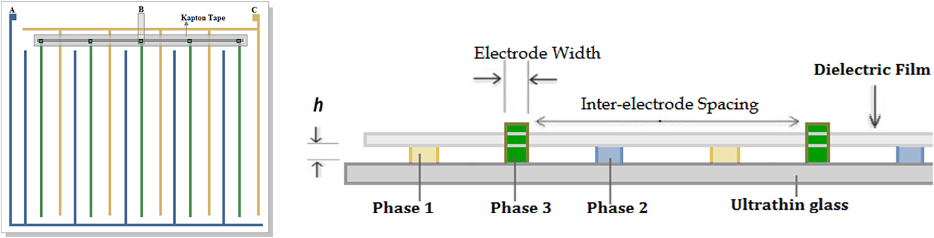
Figure 1. Schematic diagram of the parallel electrode geometry of an EDS film (a). Three-phase connections of electrodes printed on ultrathin glass as the superstrate. The configuration shown here is the upside down position where the optical path is air-dielectric film-electrode-OCA film-solar collector (center) EDS film retrofitted on the PV cell (b).
The reflective electrodes are printed with an opaque, reflective silver ink, while the transparent electrodes are printed predominantly with silver nanowire ink. Experiments have been conducted using aluminum-doped zinc oxide (AZO) as the transparent conductive ink, but the stability of the electrodes was poor in comparison with the silver nanowire ink.
Reflectivity of electrodes of the EDS film
Oftentimes, CSP installations have mirrors that have curved surfaces or trough-like structures that cannot be cleaned by robotic devices and also heavily depend on demineralized water for the cleaning process. In the interest of retrofitting the EDS film on CSP mirrors, the electrodes are printed on flexible ultrathin glass or PET films. Silver paste ink Loctite ECI 1011 purchased from Henkel Electronics is used to print the electrodes of the EDS film as it has very high reflectivity when compared to other commercially available inks. The reflective EDS films are tested for their specular reflectivity (SR) and for the specular reflectivity restoration (SRR) factor, given by
 $${\rm{SRR}} = {{{\rm{S}}{{\rm{R}}_{\rm{i}}}} / {{\rm{S}}{{\rm{R}}_{\rm{o}}}}},$$
where SRi is the specular reflection after EDS panel activation, and SRo is the specular reflection before EDS panel activation. SRR determines how much of the SR is restored upon EDS panel activation, after a soiling scenario. Ideally, SR must be above 90% and SRR must be above 95%.
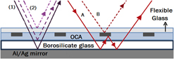
The electrodes of the EDS film, which are applied to the mirrors, must ideally have excellent SR both on the top surface and on the bottom surface. This would ensure that the incident sunlight on the structure undergoes minimal loss by absorption and the majority of it is reflected back to the collector. Figure 2 shows a representation of an ideal reflective electrode EDS film with borosilicate glass as a supporting structure.
Figure 2. Schematic diagram of the parallel electrode geometry for an EDS film with reflection pattern of incident light on different layers: (1) Primary reflections, (2) secondary reflections, (A) reflection from the bottom electrode surface, and (B) reflection from the top surface of the electrode.
Taking into consideration that the method needs to be scalable to large area power plants and should be cost-effective, the production of the EDS film is largely based on screen printing. The method is then translated to flexographic printing as a transition from lab scale to roll-to-roll industrial production scale. Screen printing of the reflective silver ink renders a smooth surface on the bottom of the electrode as it is pressed on the borosilicate substrate, thereby allowing uniform alignment of the silver particles in the ink solution. The top surface of the electrode remains exposed to air and its surface profile results to be highly rugged upon curing the ink at high temperatures. The curing process results in the formation of craters and peaks that are left behind by the escaping volatile solvents and binders, when they nucleate and rise to the surface to burn off,Reference Bernard, Eriksen, Lin, Yellowhair, Garner, Sayyah, Griffin, Lloyd, Gao, La Centra, Morales, Lakshmanan, Horenstein and Mazumder6 as shown in Fig. 3. Curing cannot be avoided as the binder and solvent in the ink need to burn off for the ink to become conductive in its solid state. The rough top surface of the electrodes poses a major impediment for obtaining desired elevated SR values as such a surface is seen to promote diffused reflectivity.
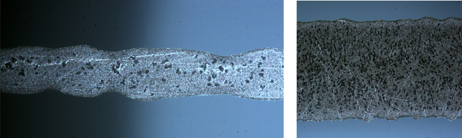
Figure 3. Image of electrode (a) and bus bar (b) of the EDS panel exposing craters formed due to organic vapors nucleating and burning off during curing in the oven at high temperatures.
Experiments to improve reflectivity of electrodes
To render the top surface as smooth and uniform, polishing the electrodes with microbrushes was attempted. This led to scratching the electrodes and produced breaks through the entire length of the electrode since the height of the electrodes is ∼3 µm. The alternative efforts followed to improve SR are listed below.
Curing temperature alteration
For this experiment, EDS panels were produced using the same reflective silver ink, all screen-printed at the same time and then were introduced to varying temperature environments. Experiments were conducted with varying the curing procedure,
(i) EDS film cured at 200 °C in a lab convection oven for 30 min.
(ii) EDS film allowed an initial slow cure period of 8 h maintained at room temperature (25 °C).
(iii) EDS film subjected to rapid cooling cure period of 10 h at 4 °C.
The variation in the curing period corresponds to the time taken for each of the samples to have solid electrodes.
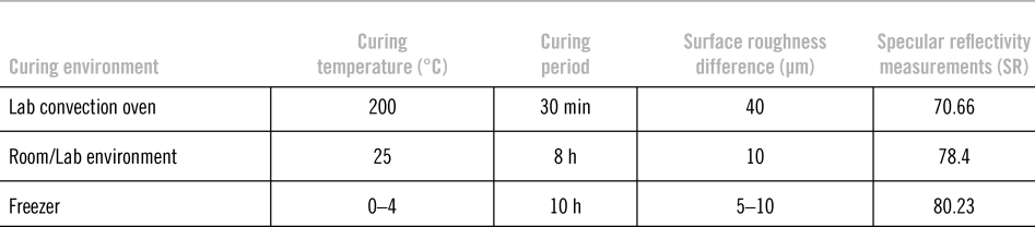
For the EDS films that were not oven cured, the silver particles in solution were seen to align more uniformly and the surface profile of such an electrode showed much smoother surfaces. The electrodes, however, were not conductive. Slow curing followed by curing the EDS film at 185 °C in a lab convection oven resulted in conductive electrodes with negligible loss in surface smoothness and SR. Measurements taken with the Alpha step 500 KLA Tencor surface profiler (Milpitas, California) demonstrated the difference in surface uniformity of the samples that were cured in different temperature settings. It is seen that the samples subjected to rapid cooling exhibit the least number of peaks and least height difference between them. The difference in the heights of the craters and peaks for each of these settings and the corresponding SR values are provided in Table 1.
Table 1. Summary of variations of curing techniques.
Addition of silver nanoflakes—hybrid ink
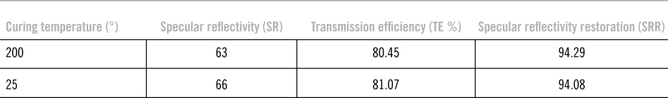
The silver particles in the reflective ink solution are silver microspheres in the size range of >1 mm in diameter. Upon screen printing and post curing, the electrodes have beaded and discontinuous structures, observed under a microscope. To promote uniformity in particle spread and alignment on the top surface, silver nanoflakes in the size range of 1–3 µm were added to the reflective silver ink, in solution form, upon mixing with solvent DBE-9 (Sigma-Alrich, Burlington, Massachusetts). Various ratios of silver nanoflakes [percentage by weight (wt%) in solution] were evaluated for screen printability and each trial solution was mixed with a standard volume of reflective silver ink. The experiment on varying the curing temperature was also performed on the hybrid ink samples.
The EDS panels produced by printing with the hybrid ink resulted in lower SR values. On inspecting the samples under the microscope and surface profiler, it was seen that the particle alignment was random and dense, but not uniform, and hence the surface of electrodes exhibited increased diffuse reflectivity. The SRR measurements of these EDS films were higher than those with plain reflective silver ink and meet the ideal SRR expectancy. This is hypothesized to be due to the increased continuity of the electrodes and denser packing of silver, hence clearing more dust than the plain electrodes with reduced continuity. Table 2 displays the SR and SRR values of the EDS films produced as a result of this experiment.
Table 2. SR and SRR of hybrid ink electrodes.
Electroplating and electroless-plating
Test panels were made by screen printing the borosilicate glass substrate with reflective silver ink as (i) uniform continuous film and (ii) standard EDS films that were both cured at 200 °C and were subjected to both electroplating and electroless-plating with siver nitrate and brighteners as active agents. The experiments were performed in our laboratory and also outsourced to a company, to have a comparative evaluation. The resulting substrates exhibited a slight decrease in SR values. This is believed to be a result of the nonuniform topography of the initial substrate, i.e., the surface roughness of the film before subjecting to electroplating/electroless-plating was nonuniform. The measured surface peaks had a height difference of nearly 1 µm between peaks. Thus, plating on such rugged surfaces would result in promoting the roughness by increased rugged deposition of the active agent.
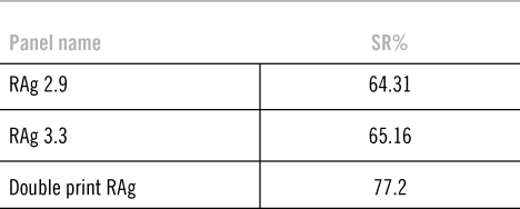
EDS panels produced via the photolithography process in the laboratory have shown minimal surface roughness, in the order of 0.01 to 0.015 µm in height difference between peaks (Table 3).
Table 3. SR% comparison of different samples printed with reflective silver ink.
Ongoing and future experiments to improve SR
Double print structure
The EDS film pattern was screen printed on borosilicate glass, using reflective silver ink (RAg) as customary. Electrodes of the same geometry were screen printed on ultrathin glass using the same ink. Both structures were cured so as to render the ‘bottom’-side reflective. The ultrathin glass was then aligned with the borosilicate glass using silicon encapsulant as adhesive so that the electrodes were precisely on top of each other. Hence, the electrode now has both surfaces as reflective, as shown in Fig. 4. The SR reading was found to be considerably higher than any other EDS films as shown in Table 3. The structure is to be repeated by replacing the borosilicate glass with ultrathin glass and using liquid optically clear adhesive instead of silicon encapsulant, thereby providing a higher transmission efficiency.
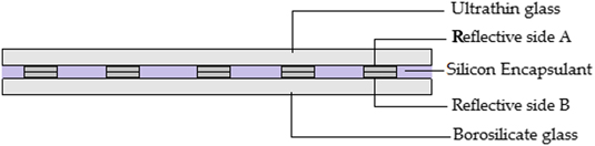
Figure 4. Double print structure of EDS panel where the electrodes have reflective surfaces on the top and bottom.
Silver nanoflakes hybrid ink
Silver nanoflakes with particle size as 300 nm and silver solution that has silver nanospheres with diameters of 10–30 nm will be obtained from Tokusen. The particle size range is remarkably finer than the silver flakes used in the previous experiments. Hence, repeating the experiments will produce better results for SRR.
These particles, when sintered at very high temperatures, will produce a smooth and uniform layer,Reference Voué, Dahmouchène and De Coninck7 which cannot be done with the nanoflakes previously used, as their particle size is too large for the sintering to occur. Thus, the ongoing and future experiments are projected to yield high SR and SRR values.
Layered electrode structure
Studies have shown that forming a layered structure with aluminum and silver could extend the reflectivity of silver when light below 400 nm wave length. The process of encapsulating the layered structure with NiCrNx has shown to provide resistance against corrosion and prevents the silver from tarnishing from sulfur or oxygen.Reference Chu, Fuqua and Barrie8,Reference Folgner, Chu, Lingley, Kim, Yang and Barrie9 The ongoing experiment includes depositing the NiCrNx to encapsulate the layered Al–Ag structure and then patterning it to produce an EDS film.
Auxiliary methods to improve SR
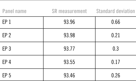
An alternative method of producing EDS film is through photolithography. Experiments were conducted with chromium as the electrode material and 5 EDS panels were made via photolithography. These panels were then subjected to electroplating. SR measurements were conducted on all 5 panels with data points from 10 trials each. Table 4 represents the SR values obtained from them along with the corresponding standard deviation for 10 trials. The EDS panels were of standard geometry and produced in comparable conditions. The measurement results from each panel are identical to the other panels, which reinforce consistency.
Table 4. SR measurement results from test panels.
Though photolithography process is deemed unscalable to the size of the solar and thermal power plants, but can be used to explore techniques that can achieve elevated values of SR, which then would be translated to screen printing, GOP, or flexographic printing. Thus, when proof of concept is achieved via photolithography, modifications in production can be done to make the suggested methods convertible to scalable methods for mass production. A headway spinner can be used to spin coat silver nanoparticles in solution on the borosilicate glass substrate. Spin coating ensures uniform spreading of the particles in solution, which would give a continuous film of the deposited material. This film can then be patterned into an EDS film by suitable photolithography methods.
Durability of EDS on field
A set of 4 test standard EDS panels were subjected to field testing as shown in Fig. 5, to determine the stability and durability of the panels and to assess the functionality of EDS films in an environment outside lab settings. The tests were performed in the Atacama Desert of Chile, within a 2 km radius of existing solar power plants. The EDS panel was programmed to operate once a day for 1 min duration. The set-up was also placed at a mining area where the panels were exposed to finer dust particles. The third location of testing was near a beach, thereby subjecting the EDS film to saline environments with high humidity. The complete cycle of testing included rainfall, desert environment, and saline environment without any periodic manual cleaning of the panels. The EDS panels proved to be stable, durable, and fully functional in all the testing conditions. The duration of the test period was over 3 months. The measurements, listed in Table 5, show the output power restoration (OPR) capacity of the EDS films when retrofitted onto PV cells. OPR measures the restoration of the output current derived from the PV cells upon activation of the EDS in a soiling scenario. A second test unit is being set up, to confirm the success of the previous tests. The duration of the second test set-up will be for over 6 months and EDS activation would be varied to 2 min each week to observe if successful results would be produced (Table 5).
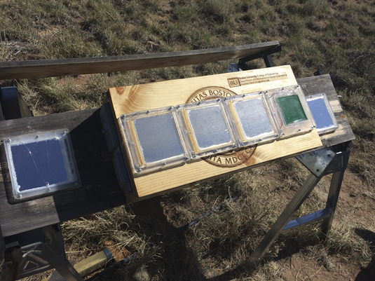
Figure 5. EDS film with reflective electrodes on field test site.
Table 5. Performance of EDS in outdoor setting for OPR.

Conclusion
To reduce the operation and maintenance (O&M) cost of large-scale solar and thermal energy harvesting plants, it is necessary to utilize a low-cost, durable, automated, and self-cleaning system with minimal water usage. EDS film is an emerging technology for self-cleaning solar collectors being developed to maintain high optical efficiency of concentrating mirrors, receivers, and PV modules. The electrodynamic dust removal method has a strong potential for maintaining high efficiency of solar collectors with minimum usage of water and at a low O&M costReference Joglekar, Guzelsu, Mazumder, Botts and Ho10 and will prove to be beneficial, if not necessary, for large-scale applications of solar energy meeting global demand. Studies show that transparent and reflective EDS can be integrated on the surface of solar mirrors to maintain specular reflection efficiency greater than 90%. The method is applicable for both parabolic troughs and heliostat mirrors. Production of the EDS films by gravure offset printing and flexographic printing indicate the potential of scale-up and high volume production. Evaluations performed under simulated desert and semi-arid conditions and on field tests show that the EDS-based dust removal process is able to maintain high optical efficiency with low energy requirements.
Acknowledgments
We acknowledge the grant from the Department of Energy (DOE CSP APOLLO EE-0007119) for supporting this research project on “Enhancement of Optical Efficiency of CSP Mirrors for Reducing O&M Cost via Near-Continuous Operation of Self-Cleaning Electrodynamic Screens (EDS)”. Support from MassCEC for a cost-sharing grant on the project is acknowledged. We also acknowledge the support from our partners including Corning Research & Development Corporation, Industrial Technology Research Institute (ITRI), GeodrillR (EDS Chile SpA), and Sandia National Laboratories.


