Hostname: page-component-848d4c4894-p2v8j Total loading time: 0 Render date: 2024-05-06T23:17:49.742Z Has data issue: false hasContentIssue false

Quantitative in-situ TEM study of stress-assisted grain growth

Published online by Cambridge University Press:  15 April 2013

Sandeep Kumar*
Affiliation:
Department of Mechanical Engineering and Program in Materials Science and Engineering, University of California, Riverside, California 92521
Tarek Alam
Affiliation:
Mechanical and Nuclear Engineering, Penn State University, University Park, Pennsylvania 16802
Aman Haque
Affiliation:
Mechanical and Nuclear Engineering, Penn State University, University Park, Pennsylvania 16802
*
Address all correspondence to Sandeep Kumar atskumar@engr.ucr.edu
Get access

Abstract

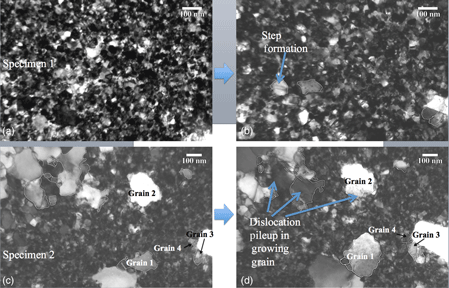
We present a quantitative in-situ transmission electron microscope (TEM) study of stress-assisted grain growth in 75 nm thick platinum thin films. We utilized notch-induced stress concentration to observe the microstructural evolution in real time. From quantitative measurements, we find that rapid grain growth occurred above 290 MPa of far field stress and ~0.14% elongation. This value is found to be higher than that required for stable interface motion but lower than the stress required for unstable grain boundary motion. We attribute such grain growth to geometrical incompatibility arising out of crystallographic misorientation in adjoining grains, or in other words, geometrically necessary grain growth.

Type
Research Letters
Copyright
Copyright © Materials Research Society 2013 

Access options

Get access to the full version of this content by using one of the access options below. (Log in options will check for institutional or personal access. Content may require purchase if you do not have access.)

References

1Wang, N., Wang, Z., Aust, K.T., and Erb, U.: Effect of grain size on mechanical properties of nanocrystalline materials. Acta Metall. Mater. 43, 519 (1995).Google Scholar
2Wang, Y.B., Li, B.Q., Sui, M.L., and Mao, S.X.: Deformation-induced grain rotation and growth in nanocrystalline Ni. Appl. Phys. Lett. 92, 011903 (2008).Google Scholar
3Haslam, A.J., Moldovan, D., Yamakov, V., Wolf, D., Phillpot, S.R., and Gleiter, H.: Stress-enhanced grain growth in a nanocrystalline material by molecular-dynamics simulation. Acta Mater. 51, 2097 (2003).Google Scholar
4Shan, Z., Stach, E.A., Wiezorek, J.M.K., Knapp, J.A., Follstaedt, D.M., and Mao, S.X.: Grain boundary-mediated plasticity in nanocrystalline nickel. Science 305, 654 (2004).Google Scholar
5Gianola, D.S., Van Petegem, S., Legros, M., Brandstetter, S., Van Swygenhoven, H., and Hemker, K.J.: Stress-assisted discontinuous grain growth and its effect on the deformation behavior of nanocrystalline aluminum thin films. Acta Mater. 54, 2253 (2006).Google Scholar
6Haque, M.A. and Saif, M.T.A.: Mechanical behavior of 30–50 nm thick aluminum films under uniaxial tension. Scr. Mater. 47, 863 (2002).Google Scholar
7Haque, M.A. and Saif, M.T.A.: Deformation mechanisms in free-standing nanoscale thin films: a quantitative in situ transmission electron microscope study. Proc. Natl. Acad. Sci. 101, 6335 (2004).Google Scholar
8Kumar, S., Haque, M.A., and Gao, H.: Notch insensitive fracture in nanoscale thin films. Appl. Phys. Lett. 94, 253104 (2009).Google Scholar
9Kumar, S., Alam, M.T., and Haque, M.A.: Fatigue insensitivity of nanoscale freestanding aluminum films. J. Microelectromech. Syst. 20, 53 (2010).Google Scholar
10Kumar, S., Li, X., Haque, A., and Gao, H.: Is stress concentration relevant for nanocrystalline metals? Nano Lett. 11, 2510 (2011).Google Scholar
11Sharon, J.A., Su, P.C., Prinz, F.B., and Hemker, K.J.: Stress-driven grain growth in nanocrystalline Pt thin films. Scr. Mater. 64, 25 (2011).Google Scholar
12Kumar, S., Alam, M.T., Connell, Z., and Haque, M.A.: Electromigration stress induced deformation mechanisms in free-standing platinum thin films. Scr. Mater. 65, 277 (2011).Google Scholar
13Gao, B., Rudneva, M., McGarrity, K.S., Xu, Q., Prins, F., Thijssen, J.M., Zandbergen, H., and Zant, H.S.J.v.d.: In situ transmission electron microscopy imaging of grain growth in a platinum nanobridge induced by electric current annealing. Nanotechnology 22, 205705 (2011).CrossRefGoogle Scholar
14Zhu, Y. and Espinosa, H.D.: An electromechanical material testing system for in situ electron microscopy and applications. Proc. Natl. Acad. Sci. 102, 14503 (2005).Google Scholar
15Haque, M.A. and Saif, M.T.A.: Application of MEMS force sensors for in situ mechanical characterization of nano-scale thin films in SEM and TEM. Sens. Actuators A 97–98, 239 (2002).Google Scholar
16Zhu, Y., Corigliano, A., and Espinosa, H.D.: A thermal actuator for nanoscale in situ microscopy testing: design and characterization. J. Micromech. Microeng. 16, 242 (2006).Google Scholar
17Kumar, S., Wolfe, D.E., and Haque, M.A.: Dislocation shielding and flaw tolerance in titanium nitride. Int. J. Plast. 27, 739 (2011).CrossRefGoogle Scholar
18Baratta, F. and Neal, D.: Stress-concentration factors in u-shaped and semi-elliptical edge notches. J. Strain Anal. Eng. Des. 5, 121 (1970).Google Scholar
19Gutkin, M.Y. and Ovid'ko, I.A.: Grain boundary migration as rotational deformation mode in nanocrystalline materials. Appl. Phys. Lett. 87, 251916 (2005).CrossRefGoogle Scholar
20Cahn, J.W., Mishin, Y., and Suzuki, A.: Coupling grain boundary motion to shear deformation. Acta Mater. 54, 4953 (2006).Google Scholar
21Winning, M., Gottstein, G., and Shvindlerman, L.S.: On the mechanisms of grain boundary migration. Acta Mater. 50, 353 (2002).Google Scholar
22Winning, M., Gottstein, G., and Shvindlerman, L.S.: Stress induced grain boundary motion. Acta Mater. 49, 211 (2001).Google Scholar
23Sansoz, F. and Dupont, V.: Grain growth behavior at absolute zero during nanocrystalline metal indentation. Appl. Phys. Lett. 89, 111901 (2006).Google Scholar
24Horton, J.A. and Ohr, S.M.: TEM observations of dislocation emission at crack tips in aluminium. J. Mater. Sci. 17, 3140 (1982).Google Scholar
25Zielinski, W., Lii, M.J., and Gerberich, W.W.: Crack-tip dislocation emission arrangements for equilibrium – I. In situ TEM observations of Fe–2 wt%Si. Acta Metall. Mater. 40, 2861 (1992).Google Scholar
Supplementary material: Image

Kumar et al.supplementary material

Supplementary figs

Download Kumar et al.supplementary material(Image)
Image 660 KB