Introduction
The scanning tunneling microscope (STM), invented by Gerd Binnig and Heinrich Roher at IBM Zurich in 1986 [Reference Binnig and Rohrer1], is an essential tool in nanoscience and nanotechnology. In an STM, a nanoscale metal tip electrode is brought within 0.5 nm of an electrically conductive sample, and a DC bias voltage is applied to cause an electrical current to flow by quantum tunneling. Typically, a piezoelectric actuator is used to move the tip to adjust its distance from the sample as the tip is scanned to create images of the sample surface. The exponential sensitivity of the tunneling current to the tip-sample distance enables sub-nanometer resolution for images at the atomic level.
Others have written software to simulate the operation of an STM for classroom demonstrations [Reference Rebello2] or created a simulator that may be downloaded for a trial period to demonstrate their product for imaging with an STM [3]. We have developed a LabVIEW Virtual Instrument (VI), which simulates the full operation of an STM that may be downloaded from our company website for permanent use without registration, cost, or time limits [4]. A 24-page description documenting the software and a video showing typical operation of the new simulator VI are also available at the website. The documentation includes figures, equations, and definitions of the terminology. We hope that this simulator VI will be useful in educational and training purposes. The STM simulator VI was compiled using LabVIEW Application Builder, which allows stand-alone applications to be bundled with the LabVIEW Run-Time Engine as an installer without requiring LabVIEW or other software. Our application was compiled to run on a Windows operating system; if requested, we will modify the STM simulator VI for use on Mac operating systems. Figure 1 shows the main display screen of the STM simulator VI when imaging silicon (100) unreconstructed. This article briefly describes the operation of the simulator and some of its features.
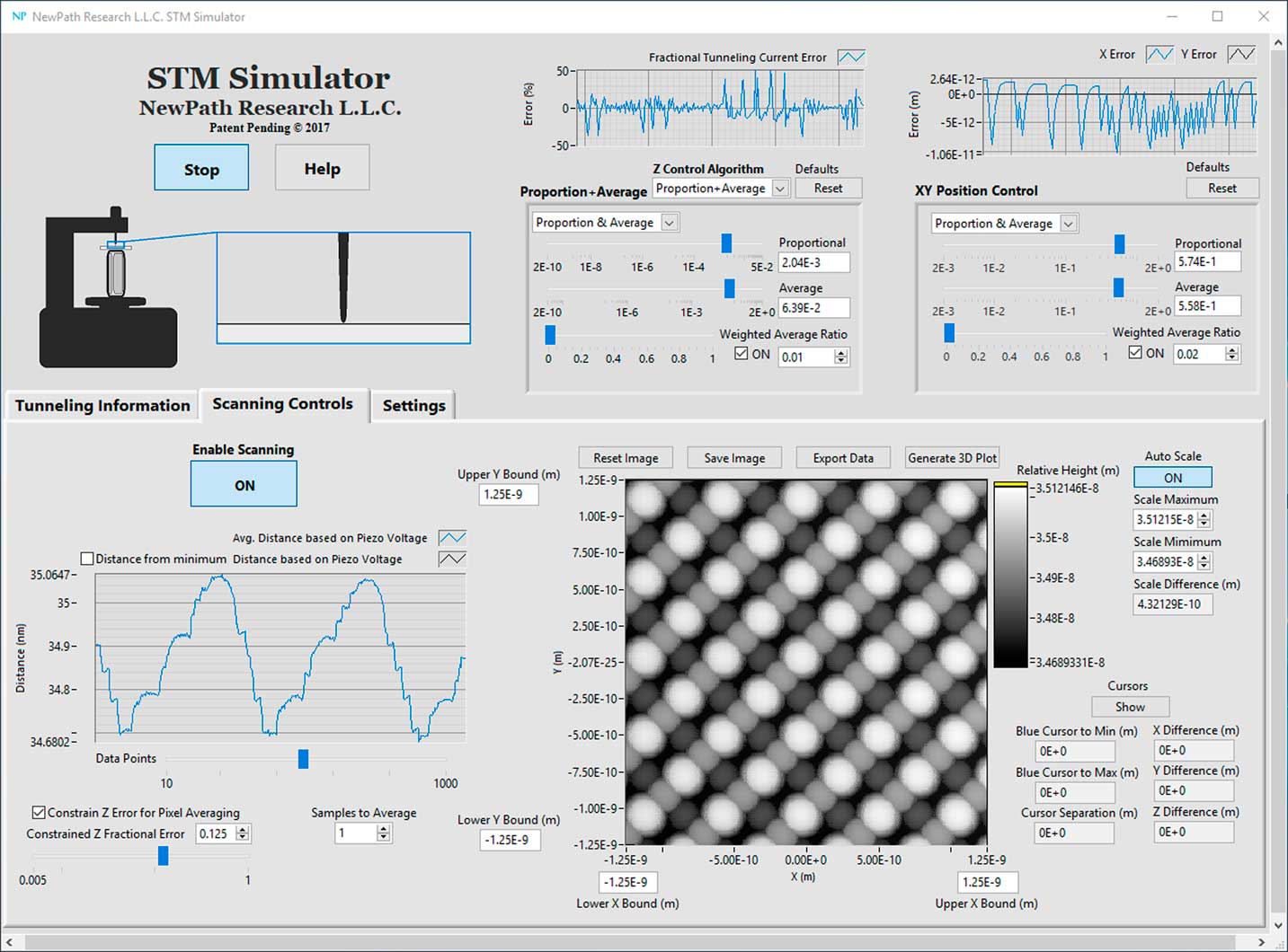
Figure 1 Main display screen of the new STM simulator VI during operation. The main screen shows the unreconstructed surface of the (100) plane of silicon. Image width = 2.5 nm.
Materials and Methods
Modeling of non-ideal phenomena
To our knowledge this is the first STM simulator to include the effects of noise in the tunneling current, noise in the voltages controlling the x-, y-, and z-motions of the piezoelectric actuator, and stochastic slow-drift in the vertical position of the tip electrode, which would be caused by vibration and temperature changes.
The effects of a series resistance, such as the spreading resistance in the sample at the tunneling junction, are also included. Bounds for these non-ideal behaviors may be set by the user to determine their effects on measurements and imaging. The software is written in a modular format to facilitate upgrading different parts to better meet our needs and also to follow the suggestions from those who have downloaded this simulator VI. For example, we could model the resonances, nonlinearities, and hysteresis in the response of the piezoelectric actuator, which is used for fine-positioning of the tip electrode and may also provide different approximations to calculate the tunneling current including expressions for semiconductor samples.
Four methods for feedback control
Feedback control is used to adjust the tip-sample distance in an STM when initiating quantum tunneling and then to minimize the error in the tunneling current, which is given by e(t) = I(t) – ISP, where I(t) is the current at time t and ISP is the chosen value for the set-point current. Simply making a change in the voltage ΔV to the piezoelectric actuator that is proportional to the error is insufficient because this would cause the tunneling current to oscillate about the set-point value.
PI (Proportion + Integral) feedback control, where the change in the voltage that is applied to the piezoelectric actuator is proportional to the sum of the error and the integral of the error, as shown in Eq. (1), is frequently used in scanning tunneling microscopy.
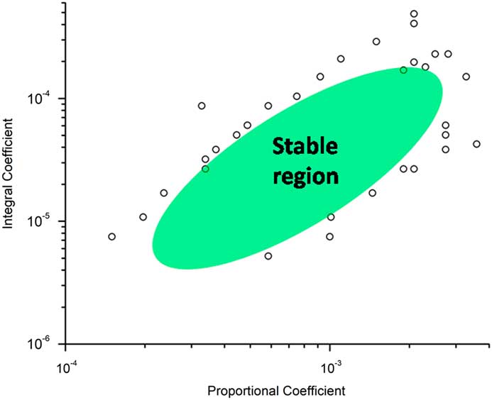
Simulations made with the STM simulator VI show that PI feedback control is only stable over a specific range for the two coefficients K P and K I (see Figure 2). The size and location of the stable region for these two coefficients depends on the properties of the tip and the tip-sample distance. Large oscillations in the tunneling current, including the possibility of tip-crash failure or loss of tunneling, occur when one (or both) of these coefficients is outside of the region for stability. It is inconvenient to have to estimate the value for both coefficients before the measurements.

Figure 2 Stable region for the two coefficients controlling PI feedback of the tunneling current.
The included algorithms are: (1) Unmodified PI as previously described, (2) D.A.S. (Digitally Adapted Steps), which adjusts the sizes of the steps of the piezoelectric actuator based on the tunneling current, (3) Modified Proportion, in which the proportion coefficient is adjusted based on the tunneling current, and (4) Proportion + Average, which is similar to PI control, but instead of integrating it takes the mean of the last few values of the error. Each of these algorithms is described in detail on our website.
The STM simulator VI may be used to compare the stability, response time, and ease of use for feedback control of the current when using the four different algorithms with various values for their parameters.
Stepper motor and piezoelectric actuator
To obtain atomic resolution in imaging, the piezoelectric actuator must have a small range of motion (typically 60 nm). Thus, it is necessary to add a precision digital stepper motor for coarser positioning of the tip electrode in order to provide a greater range of motion in the system. The piezoelectric actuator is automatically decremented each time before the digital stepper motor is incremented to avoid missing specific tip-sample distances, which would be caused by the effects of the finite precision of the step motor.
Simulation of crystal lattice sufaces in real time
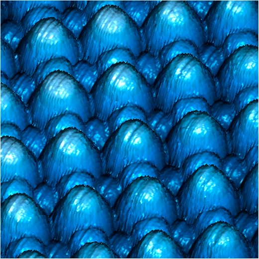
Once the simulation shows that stable quantum tunneling has been achieved, it is possible to generate an image of highly ordered pyrolytic graphite (HOPG), graphene, silicon (100) unreconstructed, or the reconstructed surface of silicon after it has been cleaved. The surfaces of these four materials were modeled by approximating the contours for the local density of states of electrons in the atoms as spheres with appropriate sizes. The images of the surfaces are created by scanning over the simulated surfaces while calculating the tunneling current based on the distance from the surface to the tip. Figure 1 shows the main display screen when simulating the imaging of silicon (100) unreconstructed. The graph at the lower left corner of this figure shows the relative height of the tip, which is calculated from the voltage that is applied to the piezoelectric actuator. Oscillations in the height, which are seen in this graph, are caused by the tip electrode passing over several of the silicon atoms in the lattice.
At the upper left corner of Figure 1 there is a sketch of the STM scan-head with an animated diagram showing the vertical tip electrode above the horizontal sample. If the value calculated for the tip position is below the surface of the sample, indicating a tip-crash has occurred, this cartoon shows that the tip is bent and the simulation has stopped. However, with an actual STM it may not be obvious that a tip-crash has occurred because images with high resolution are still possible. Thus, this feature enables the user to determine the optimum parameters to prevent tip-crash. Later we will incorporate an algorithm to determine if a tip-crash has occurred without relying on the simulated height of the tip. For example, a small increment in the voltage to the piezoelectric actuator would not change the current when the tip is in contact with the sample. This change would be necessary before the STM simulator VI software could be implemented in an actual STM.
In the constant current mode, feedback control of the tunneling current is enabled during scanning. In the constant height mode, feedback control is disabled during scanning so that the tip is moved in a plane above the surface of the sample. This mode is prone to loss of tunneling or tip-crash unless it is used to image small areas or with samples having relatively flat surfaces.
Results
Figure 3 shows a graph of the simulated tunneling current over a specific time interval, which is incremented throughout each session. This figure shows the effects of the noise in the tunneling current. A separate plot that is made over a much longer time interval is used to monitor the effects of feedback control on the tunneling current as well as the response to the simulated stochastic slow-drift.
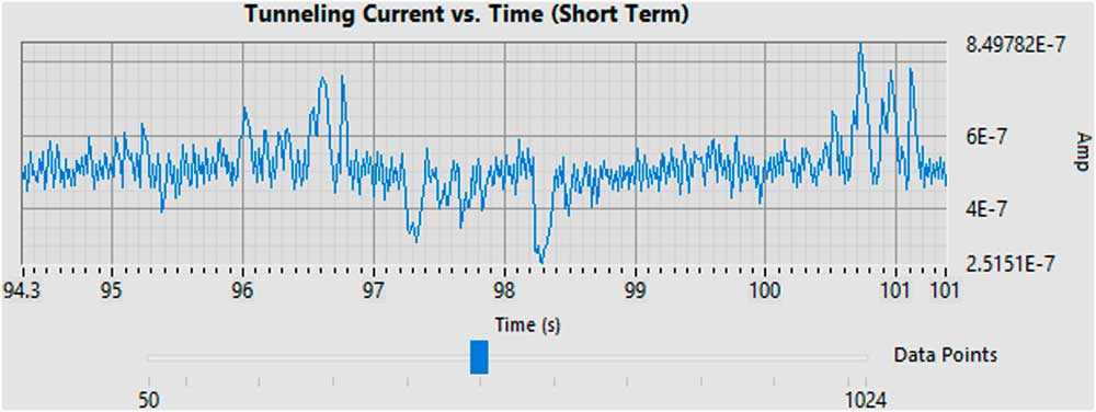
Figure 3 Graph of the simulated tunneling current vs. time showing the noise in the tunneling current.
After at least one line of a scan has been completed, a 3D image of the sample may be generated as the data are collected for an image. Figure 4 shows an example of a completed 3D simulated image of silicon (100) unreconstructed.
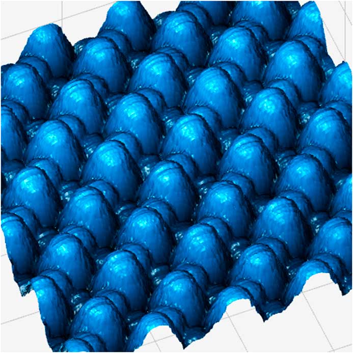
Figure 4 3D plot of a simulated image of silicon (100) surface unreconstructed.
Discussion
The virtual instrument described in this article is our first step in developing a prototype instrument, which is based on laser-assisted scanning tunneling microscopy. This work is funded by the National Science Foundation as part of a project to develop a new means for carrier profiling to meet the needs of the semiconductor industry at the new sub-22 nm lithography nodes [Reference Hagmann5]. This project is based on an earlier project funded by the U.S. Department of Energy in which a microwave frequency comb, with hundreds of harmonics at integer multiples of the laser pulse-repetition frequency, was first generated by laser-assisted tunneling [Reference Hagmann6].
Our next step in this project is to prepare a second LabVIEW VI to simulate our procedure for carrier profiling, which will also be placed on the company website as a free-download.
After the second STM simulator VI is completed, we will finish the prototype by combining the two VIs with our in-house STM in a field-programmable gate array (FPGA)-based measurement system. It is our objective to create a prototype in which each physical component of the system (for example, laser, STM scan-head, current preamplifier, microwave spectrum analyzer, etc.) may be separately exchanged with its simulator. This will provide real-time deterministic control of multiple simultaneous functions and facilitate the assembly, maintenance, debugging, characterization, and optimization of the prototype.
Conclusion
This article describes a LabVIEW-based virtual scanning tunneling microscope (STM) that is available as a free-download at our company website. This software simulates the full operation of an STM including imaging at the atomic scale.