


Introduction
Since the creation of the Joint Committee on Powder Diffraction Standards (JCPDS) over sixty years ago, the Powder Diffraction File (PDF) has been the key source of standard powder diffraction data for identification and analysis of materials of all types, from natural minerals and high-tech ceramics to metals and alloys and pharmaceuticals [Reference Faber and Fawcett1]. Although this editorially reviewed database has been the mainstay for diffraction pattern reference for the x-ray powder diffraction community, recent developments provide information and tools for electron diffraction. In recent years, the International Centre for Diffraction Data (ICDD, formerly JCPDS) has transformed the flat-file format of the PDF to a more flexible relational database (RDB) format. The PDF has been greatly expanded to include calculated patterns from multiple collaborating databases, including the Inorganic Crystal Structure Database (FIZ Karlsruhe, Germany), the Linus Pauling File (MPDS, Vitznau, Switzerland), and the Cambridge Structural Database (CCDC, Cambridge, United Kingdom) [Reference Faber and Fawcett1, Reference Kabekkodu, Faber and Fawcett2]. A significant portion of its entries include atomic coordinates and a specific database dedicated to organic phases exists [Reference Needham and Faber3]. All new entries for the ICDD databases undergo over 100 quality checks before inclusion, and a quality mark is assigned for each entry that passes.
Recently, the ICDD has developed software tools for the simulation of 2-dimensional (2D) electron diffraction patterns. Currently, three different types of 2D electron diffraction patterns can be simulated with this software: selected area electron diffraction (SAED) patterns generated for single crystals in the transmission electron microscope (TEM), ring patterns generated for polycrystalline materials in the TEM, and electron backscatter diffraction (EBSD) patterns typically obtained using a scanning electron microscope (SEM). These electron diffraction simulation tools have been implemented in the DDView+ software included with the PDF-4 series of databases. These electron diffraction tools connect to more than 660,000 entries in the current version of these databases. Each of these simulation tools is discussed below and illustrated with examples prepared using the PDF-4+ 2010 database with DDView+ software.
Selected Area Electron Diffraction (SAED) Spot Patterns
The ability to simulate SAED patterns has valuable implications for the researcher. These include the use of such patterns to verify the phase identity and crystal symmetry of target materials and to determine the orientation of crystallites in the material. Additionally, one can examine the effect of sample synthesis conditions or post-synthesis treatment by comparing the sample's experimental SAED pattern to a pattern simulated for a “standard” material.
The simulation of SAED patterns was introduced to the PDF in 2006, based on programming originally developed, and kindly provided, by R.P. Goehner [Reference Rao and Goehner4, Reference Goehner and Rao5]. At that time only the spot positions were simulated from the crystallographic information in the database with no intensity estimation. Subsequent software releases approximated, and later calculated, intensities for the spots.
SAED pattern intensities are simulated three different ways from the PDF: (a) For entries with included structural atomic coordinates, the diffracted intensities are calculated on-the-fly from the structural model using scattering factors based on the user-supplied electron wavelength. (b) For other entries where the ICDD has access to, but is restricted from distributing, structural atomic coordinates, structure factor tables have been embedded in the database; they are pre-calculated using atomic scattering amplitudes for electrons [Reference Prince6] with a beam energy of 200 keV. This allows reasonably accurate SAED simulated patterns to be calculated on-the-fly because the relative scattering factors for various elements change little when the electron beam energy is varied over a fairly broad range of values. (c) Many traditional experimental PDF entries do not have atomic coordinates with which to calculate the diffracted intensities. For these entries, SAED pattern intensities have been approximated using x-ray intensities from the PDF d-I (d-spacing/Intensity) list. For the vast majority of experimental entries, these intensities are derived from x-ray powder diffraction (XRPD) patterns, although there are a nominal number of entries prepared from neutron and electron diffraction patterns.
Figure 1 displays simulated patterns using both experimental (XRPD intensities from actual powder diffraction data, top) and calculated (intensities calculated using atomic coordinates from structural databases, bottom) PDF entries, which are compared to two observed SAED patterns (middle) for silicon-substituted alpha-tricalcium phosphate (Ca3 (PO4)2−x (SiO4)x or Si-α-TCP), a biomaterial intended for bone replacement applications [Reference Sayer, Stratilatov, Reid, Calderin, Stott, Yin, MacKenzie, Smith, Hendry and Langstaff7, Reference Reid, Tuck, Sayer, Fargo and Hendry8]. Both the experimental and calculated patterns agree fairly well with the major intensity features of the observed patterns. In general, simulated SAED patterns based on experimental XRPD intensities should be a reasonable approximation because both x-rays and electrons predominantly scatter from atomic electrons, in contrast with neutrons where scattering is primarily from the atomic nucleus. In converting powder diffraction intensities to those for single-crystal spots, the values must be divided by the reflection multiplicity. It should be noted that for the experimentally observed SAED patterns (middle), the spot intensities include dynamic contributions. This causes the appearance of kinematically forbidden reflection spots [Reference Williams and Carter9] that will not be present in the simulated patterns, which are based on pure kinematic diffraction. For example, for the [0 −1 −6] zone axis (left), the (h 0 0) reflections, with odd values of h, are absent from the simulations yet present in the observed SAED pattern.
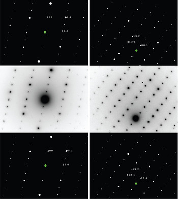
Figure 1: SAED patterns from the [0 −1 −6] (left) and [3 −1 0] (right) zone axes of silicon substituted alpha-tricalcium phosphate (Ca3 (PO4)2−x (SiO4)x, Si-α-TCP), simulated using an experimental PDF entry with ED intensities approximated using the XRD intensities (top, PDF 00-058-0897) and simulated using a calculated PDF entry for pure tricalcium phosphate with the ED intensities calculated from the atomic coordinates (bottom, PDF 04-010-4348). The observed SAED patterns (middle) were provided by Drs. Maureen MacKenzie and Michael Sayer. Using the PDF-4+ databases and included DDView+ software, SAED patterns for any zone of over 660,000 entries can be simulated.
The SAED pattern simulation window for specifying the simulation parameters is illustrated in Figure 2. These parameters, which include the zone axis, camera length (or camera constant), and voltage (or wavelength), can all be selected and edited with dynamic re-simulation of the pattern using the new values. New to the 2010 release of the PDF, real digitized SAED patterns can now be imported into the window (in JPG, GIF, and PNG formats) for comparison with the simulation. Figure 2 shows a comparison between the real and simulated [0 −1 −6] zone axis of silicon substituted alpha-tricalcium phosphate.
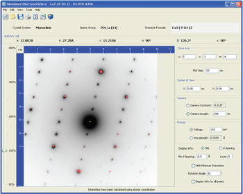
Figure 2: The simulated SAED pattern interface illustrates the user-specified parameters that can be edited for on-the-fly pattern recalculation. An actual digitized SAED pattern has been imported for comparison with the simulation. The observed SAED pattern was provided by Drs. Maureen MacKenzie and Michael Sayer.
Polycrystalline Ring Patterns
Simulation of ring patterns was a new feature in the 2009 release of the PDF-4+ database software. The ring pattern simulation provides a 2D representation of the pattern for a given polycrystalline phase as it would appear on flat 2D detectors such as photographic film, phosphor image plates, or solid-state 2D arrays. Ring patterns can be simulated for all primary beam radiation wavelengths (electron, x-ray, and neutron); however, in all cases the intensities are approximated using the values from the d-I list, usually based on x-ray intensities. The simulation assumes no preferred orientation in the specimen, axial positioning of the detector (transmission geometry with incident beam centered), and an infinite number of randomly oriented crystallites.
To simulate a ring pattern, a simulated 1D diffraction trace is created first using the d-spacings and intensities from the PDF entry. The d-spacings of the Bragg reflections are converted to diffraction angles (radians, 2θ) with the user-defined electron wave-length and the intensity profile of each individual reflection is calculated using a Gaussian function of the following form:
Here I is the intensity at position 2θ (radians), I n is the intensity of the nth reflection, 2θn is the position of maximum intensity of the nth reflection, and β is a breadth coefficient formulated from the average crystallite size (Å). The breadth coefficient of the Gaussian function is approximated using the Scherrer equation for size broadening [Reference Cullity10, Reference Guinier11], where the full width at half maximum (B) has been converted to an integral breadth (β):
Here λ is the electron wavelength (Å), t is the average crystallite size (Å), and θ is the diffraction angle. Calculation of the Gaussian profile function intensity is truncated in the peak tails when the value falls below 0.02% of the centroid intensity. The full diffraction trace is created by summing the individual intensity profiles over all reflections.
The second step in creating the ring pattern is to convert the simulated diffraction trace (not displayed) into a graphical 2D pattern consisting of rings on a simulated detector. This is done by converting each angular position (radians, 2θ) into a 2D ring of diameter, D (cm), where:
L is the user-defined sample-to-detector distance (cm).
As dictated by the Scherrer equation, smaller crystallite sizes produce broader rings. For the simulation, higher reflection profile intensities will produce brighter rings. Once the ring pattern has been graphically simulated, the user then has the option of zooming in and out or changing any of the ring pattern settings to re-simulate the pattern.
A simulated ring pattern is illustrated in Figure 3 for β-uranium oxide, UO3 (PDF 04-007-0516), with a crystallite size of 100 Å.
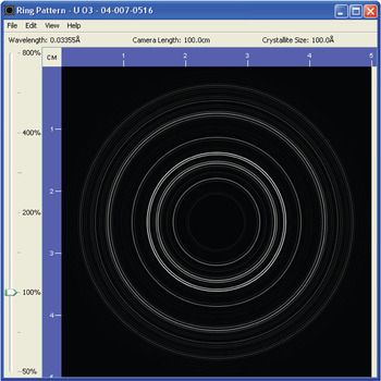
Figure 3: A simulated electron diffraction ring pattern calculated for β-uranium oxide, UO3 (PDF 04-007-0516), using an average crystallite size of 100 Å.
Electron Backscatter Diffraction (EBSD) Patterns
Electron backscatter diffraction pattern simulations were introduced to the PDF in 2006 at the same time as the SAED pattern simulations. The EBSD pattern simulations are based on programming previously described, and kindly provided, by R.P. Goehner and J.R. Michael [Reference Goehner and Michael12]. These patterns are useful in confirming phase identity, crystallite orientation, or crystalline symmetry.
New to the 2010 release of the PDF, intensity estimates have been added to the EBSD patterns. Similar to the SAED pattern simulations, the EBSD pattern intensities are either calculated on-the-fly directly from the atomic coordinates, obtained from pre-calculated structure factor tables, or approximated using the d-I list, based on the availability of atomic coordinates. The line positions are determined kinematically using unit cell parameters and space group extinction conditions associated with the PDF entry.
The EBSD simulation window is modeled on the SAED pattern simulation window. Settings such as the electron beam energy, camera length, and central zone axis can be adjusted with dynamic re-simulation of the EBSD pattern. Additional settings are provided to manipulate the orientation and size of the image, including the location of the pattern origin and rotation angle about the origin. Kikuchi line pairs can be highlighted using the cursor, with the Miller indices of the pair displayed on the pattern. A simulated EBSD pattern is illustrated in Figure 4 for copper (PDF 04-009-2090), centered on the [1 1 4] zone axis.

Figure 4: A simulated EBSD pattern for copper (PDF 04-009-2090), centered on the [1 1 4] zone axis.
Database Search Tools
To facilitate the usefulness of the PDF-4+ databases, a complete suite of search tools is available for “mining” the phases of interest from the 291,440 entries in the PDF-4+ 2009 or from the 406,773 entries in the PDF-4+/Organics 2010. Phases fitting elemental criteria, specified in either weight or atomic percentage, can be found, as can phases fitting specific crystallographic criteria, longest 1 to 10 d-spacings, common names, mineral names, etc. In fact, some 53 different fields are searchable for finding specific phases for which to simulate electron diffraction patterns.
The search tools and many of the fields in the databases were specifically developed and designed to identify unknown materials by electron diffraction techniques. Decades of work on materials identification methods by ICDD member scientists led to the developments of the Fink [Reference Smith, Beward, Berry, Post, Weissmann and Lotz13] and Matthews [Reference Smith, Beward, Berry, Post, Weissmann and Lotz14] methods for phase identification in 1963. The Fink method, specifically designed for electron diffraction, incorporated the use of long (low 2θ) interplanar spacings of high intensity as a search criterion, and the Matthews system combined interplanar spacing information with chemistry. In 1989, a team from Sandia National Laboratories, the ICDD, and the National Institute of Standards and Technology (NIST) developed the Elemental and Interplanar Spacing Index (EISI) with an electron diffraction database [Reference Himes, Mighell, Stalick, Young, Carr, Lyman, Anderson, Holomany and Jenkins15, Reference Carr, Chambers, Melgaard, Himes, Stalick and Mighell16]. The EISI allowed combined searches that incorporated elements, unit cells, space groups, chemical names, and formulas. All these search tools, developed by practicing scientists in the field, have been incorporated into the data mining capabilities of the PDF-4 databases.
To zero in on the example given in Figure 1, one could search for all entries containing only Si, Ca, P, and O and obtain a list of 12 entries from the database that meet this elemental criterion. The output list can contain any of 85 user-selectable display fields such as formula, chemical name, Pearson symbol, cell parameters, strongest 10 and longest 10 d-values, space group, etc., from which the entry of interest can be selected for electron diffraction simulation or further study.
Future Developments
Electron diffraction simulation tools in the PDF software have been evolving since the first tools were released in 2006. It is expected that new capabilities will be added in subsequent PDF releases. A number of potential new features are currently being investigated.
The ability to import real digitized data, as currently implemented for SAED patterns, may be investigated for polycrystalline ring patterns and EBSD patterns. Calculated intensities may also be investigated for polycrystalline ring patterns in cases where the atomic coordinates are available.
The potential for additional functionality beyond pattern simulation is being investigated for SAED patterns. Now that actual digitized patterns can be imported, reflection positions, angles, and intensities could also be extracted from the patterns and employed for automated indexing procedures to obtain zone axes for known phases [Reference Goehner and Rao5] or simultaneous identification of the phase and the zone axis [Reference Hart17]. Optimized search strategies specifically for electron diffraction are being considered for implementation in the PDF's SIeve+ search-match module.
Comments and suggestions from PDF users are strongly encouraged by the authors. The electron diffraction capabilities of the PDF will continue to evolve to meet the needs of the electron diffraction community.
Acknowledgments
The authors would like to thank R. P. Goehner and J. R. Michael for their contribution of programming methodology to the SAED and EBSD pattern simulations, Maureen MacKenzie and Michael Sayer for providing the SAED patterns used as examples, John Faber for important direction during the initial implementation of the SAED and EBSD simulations, the ICDD Electron Diffraction Task Team and Subcommittee for developmental guidance, and Ron Anderson for his encouragement of this undertaking.


