


Introduction
Traditional electron detectors for scanning electron microscopes (SEMs) are the Everhart-Thornley detector located on one side of the specimen and the overhead backscattered electron detector (BSED), usually mounted under the final lens. In 2011 PulseTor introduced an efficient BSED based on scintillator/silicon photomultipler technology that is small enough to be mounted on the tip of an X-ray detector [Reference Barbi, Piemonte, Lopour and Mott1, Reference Barbi, Mott and Bono2]. The scintillator converts the electron signal to light, which is in turn converted to an electrical current in the silicon photomultiplier (SiPM). Silicon photomultipliers were initially developed in Russia in the 1990s. The review article by Dolgoshein et al. [Reference Dolgoshein3] cites much of the historical development. Following the recent work of Piemonte [Reference Piemonte4] and others, the SiPM consists of an array of many identical and independent detecting elements (microcells) connected in parallel on a common Si substrate. Each microcell is an avalanche photodiode only tens of micrometers in size.
In the PulseTor detector, each intimately coupled scintillator on photomultiplier, for simplicity, is called a scintillator on multiplier (SoM). The advantages of SoM technology include the following: (1) very small size of each individual sensing segment, (2) elimination of light guides and photomultiplier tubes (PMTs), (3) efficient face-to-face scintillator–multiplier coupling, (4) low operating voltage (30–45 volts), and (5) ability to be placed almost anywhere within the specimen chamber, even on an X-ray detector.
Locating the SoM electron detector on an X-ray detector, such as a silicon drift detector (SDD), permits a new and unique form of electron imaging, called take-off angle (TOA) imaging. TOA imaging provides an image of the sample with the same viewpoint as the X-ray signal. The advantage of this configuration is that an image along the same line-of-sight as the X-ray detector provides the best possible correlation between electron and X-ray images, matching shadowing and parallax effects. The SoM imaging device integrated with an SDD is called the PulseTor ON-X™ detector (patent pending). The ON-X™ uses a pair of SoM detectors mounted in front of the SDD, on either side of the X-ray entry region through the magnetic electron trap.
Methods and Materials
Working principle. When an electron backscattered from the sample hits the scintillator of the SoM assembly, multiple light photons are generated. When one of these photons strikes a microcell in the underlying SiPM, an avalanche multiplies the single carrier generated by the photon by a factor of one million, giving rise to a signal from the firing of one microcell. When multiple photons hit the SiPM, the avalanche takes place in each of n microcells excited by a photon. The charge delivered by the sensor is now n times that of a single microcell. The integrated charge from all fired cells is the detector current signal, which retains a direct relationship over a wide dynamic range to the number of electrons striking the scintillator. This process is shown schematically in Figure 1.
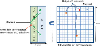
Figure 1: Diagram showing the SoM mechanism: A backscattered electron from the sample hits the YAG scintillator and emits a number of photons depending on its energy. Because YAG is transparent to light, some of the photons land on the microcells of the SiPM. Each microcell is an avalanche photodiode, which outputs a single quantum of current when it fires. If 3 microcells fire (red arrows), as in the figure, then the total device output current is 3× the current of a single microcell.
Scintillator material for the SiPM. The most common scintillator used in electron microscopy, and indeed the one selected for the ON-X™, is yttrium aluminum garnet (YAG), which emits photons in the range of 550 nm (green light). The SiPMs exhibit a broad plateau of high efficiency in the visible region of the spectrum, nearly centered at the desired 550 nm value.
SiPM and detector dimensions. Silicon photomultipliers can be made with external dimensions as small as 1 × 1 mm2 or as large as 1 × 1 cm2; however the best balance of size and performance for the ON-X™ is afforded by a device 3 mm on a side. The width dimension of each microcell within the SiPM is typically 50 microns, giving thousands of microcells within a single device. Individual SiPMs can be arrayed together to build detectors of larger size. The current SiPM comprises 3600 microcells, each 50 × 50 micron2 in size.
Figure 2 is a drawing of a detector assembly designed to fit on the collimator of an X-ray detector. The figure shows two 3 × 3 mm2 SoMs engineered to fit within the width of the electron trap/collimator, one on each side of the X-ray detector entrance. Figure 3 shows the PulseTor ON-X™ electron detector assembly mounted on an SDD detector.

Figure 2: The SoM assembly for the ON-X™ detector. Each of the sensors, marked SoM 1 and SoM 2, are square devices approximately 3 mm on a side.

Figure 3: The ON-X™ BSED mounted on an SDD X-ray detector. Inset shows a protection shroud around the two SoM assemblies.
Output signal. The out-put signal of an SiPM is a current that ultimately depends on the initial intensity of electrons hitting the scintillator. The output current is then converted to a voltage in a high-bandwidth trans-impedance amplifier, contained within the ON-X™ Video Controller (VC). The VC includes outputs for two channels, each with its own contrast and brightness controls, to enable simultaneous output of the TOA image and an annular BSED or secondary electron detector (SED) image, for example (or operation of the two ON-X™ SoMs separately). To complete the system, the output of the VC can be fed back into the SEM or into an external third-party digital image collection system, such as the Quartz XOne™ image collection system used here and offered by PulseTor.
Because the signal from the SiPM is proportional to the number of microcells that fire, the greater the number of microcells in the device, the higher the dynamic range. Ongoing development is achieving chips of the same external dimensions (3 mm × 3 mm) having more than 10,000 microcells. Because high electron intensities can produce saturation in the SiPM (the point at which all the microcells are firing), the bias applied to the SiPM can be reduced to counter saturation before it is reached. Therefore, automatic bias control is a central feature in the ON-X™ Video Controller, which can be selected to operate with fast or slow scan rates, or switched off altogether for certain experiments requiring constant bias.
Concept of Take-off Angle Imaging
Perhaps the most easily recognized example of discrepancy between X-ray maps and secondary electron (SE) images or traditional backscattered electron (BSE) images (using annular BSE detectors) can be found in an image of a simple transmission electron microscope (TEM) grid with a square mesh. If the grid is untilted (horizontal) on the specimen stage and viewed in either SE or BSE mode, it will appear with a proper square mesh. However, the X-ray detector is normally situated at an angle of 30–45 degrees to the plane of the sample, viewing the sample obliquely. The angle made by the X-ray detector centerline with respect to the plane of the sample is called the take-off angle (TOA). If the centerline of a BSE detector is made to be co-linear with the centerline of the SDD, as in the ON-X™, the electron image created is called a TOA image. Both X rays and BSEs are detected along a line-of-sight from the beam impact position to the respective detectors. When a line-of-sight BSE detector sees what the SDD sees, the BSE image looks quite different from conventional electron detector images.
Figure 4 illustrates the TOA image concept. The X-ray map is of a Cu grid on an aluminum stub. Because of the TOA viewpoint, the Al stub (blue) is partially shadowed by the Cu grid (green). The figure in the center is the TOA BSE image showing the same view as the X-ray detector. The figure on the right is the SE image showing a completely un-shadowed view from directly overhead of the specimen. It is clear from the shadowing present in the TOA image that the viewpoint of the SDD is from the bottom of the image, indicating the location of the X-ray detector with respect to the specimen.

Figure 4: X-ray map and corresponding electron images of a Cu grid on an Al specimen stub. (a) X-ray map showing that the Cu grid (green) shadows the Al (blue) specimen holder. (b) TOA image presenting the same viewpoint as the X-ray map. (c) Secondary electron image acquired with a conventional Everhart-Thornley.
The X-ray map correlates much better with the TOA image than with the SED image. This is why we describe the ON-X™/X-ray detector combination as “the SDD with Vision.” It allows the user to see what the SDD sees.
All the images shown here were acquired with a PulseTor ON-X™ SDD or a Quartz PCI XOne™ EDS system. The SEM platform was a Hitachi S3400N. All the SoM devices were made by PulseTor LLC.
Applications
Particles in a Si solar cell material.Figure 5 shows Ag-rich particles distributed in a semiconductor (solar cell) material. Figure 5a shows a 1 kV enhanced topographic image of the surface showing a prominent “pyramid” structure. Figure 5b is an overhead annular BSED image taken at 25 kV and higher magnification to show the Ag-rich particles near a pyramid. In this annular BSE image, the particles in the lower-right part of the region (within the red ellipse) appear equally prominent to those located in the upper-left part of that region. However, the lower particles are missing in both the TOA image (Figure 5c) and the Ag X-ray map (Figure 5d). The TOA image indicates that the “missing” particles are actually on the back side of a pyramid, hidden (shadowed) from the SDD perspective.

Figure 5: Ag-rich particles in a commercial solar cell material. (a) Low-magnification topographic image at 1 kV. (b) Annular BSED image at 25 kV. (c) TOA image. (d) X-ray map showing correlation of Ag (yellow) particles with the TOA image. The TOA image shows the detector perspective is from the top of the figure.
Rough metal surface.Figure 6 shows an X-ray map acquired for the Fe L line in sintered stainless steel. The TOA image correlation with the X-ray map is significantly better than the correlation between the map and the SE image. Note that the shadowed region in the upper-right of the map and the TOA image is actually a bright region in the SE image. The bright sides of certain features show that the X-ray detector, the TOA detector, and the E-T detector are all located at the top of the image.

Figure 6: Image comparison on a rough surface of sintered stainless steel. (a) Fe L line X-ray map, (b) TOA image, and (c) conventional Everhart-Thornley SE image.
Discussion
Because SoM BSED detectors require only a vacuum feed-through, several SoM detectors may be used within a single instrument, while retaining the availability of access ports for use by other detectors or devices. The ON-X™ BSED uses a feed-through built in to the SDD interface, such that no additional port is required. TOA imaging improves the correlation between electron imaging and X-ray maps, providing a complementary image mode that does not replace or preclude traditional SE or annular BSE detectors. In addition, PulseTor, in cooperation with Hitachi High-Technologies Canada, demonstrated that the SoM detector can be mounted on a micromanipulator [Reference Barbi, Piemonte, Lopour and Mott1], enabling the electron detector to be moved relative to the sample. In the cited case, sequential acquisition of backscattered electron images in reflection and in forward-scattered collection was demonstrated using the same detector.
PulseTor also has introduced a 4-segment annular detector, called the TOPaZ™, using four 4 × 4 mm2 SoMs. The name derives from the contrast mechanisms for topography and atomic number that are inherent in this type of segmented assembly. Because the four segments are controlled and processed independently, 3D imaging on any SEM is enabled using TOPaZ™ coupled with appropriate software. In a subsequent Microscopy Today article, the authors will describe the implementation of SoM technology in this more conventional configuration.
Conclusion
Silicon photomultipliers and SoM technology enable a new electron imaging mode in scanning electron microscopes. Their small size, simplicity, and high efficiency permit these BSEDs to be placed in unconventional locations in the specimen chamber: on the stage, on other detectors, on micromanipulators, or within the column itself. The specific application discussed in this article, namely integration of SoM technology with an SDD X-ray detector, enables TOA imaging with PulseTor's ON-X™ detector. The TOA imaging mode provides improved correlation between X-ray maps and SEM electron images and simplifies the interpretation of X-ray maps.
Acknowledgments
The authors wish to express their appreciation to David Bono of MIT for his contribution to product development and to Atsushi Muto of Hitachi HTA for his assistance in acquiring the results included here.


