


Introduction
The global consumer market wants smaller, faster, more reliable, lower-cost products. The semiconductor industry has responded by the doubling of chip transistor density every two years, closely following Moore's Law. To meet their goals, the industry has made huge investments in R&D and manufacturing to miniaturize components, increase the size of substrates (wafers), improve the productivity of factories, and invent new packaging technology [1].
Equipment suppliers have responded with new production and metrology tools that synthesize novel materials and measure their critical dimensions. To support this rapid development, characterization laboratories are adapting by improving capabilities and turnaround time.
As mundane as it might sound, sample preparation for analysis in the scanning electron microscope (SEM) often can be in the critical path between development engineers and the essential data they need. Given the range of sample types in silicon device technology, no single technique or laboratory tool can provide the answer for all demands, when considering accuracy, quality, throughput, ease of use, and cost. The sample preparation engineer in the laboratory must develop a process from available tools or add to the toolbox. Much effort is expended to make sure that the sample preparation process delivers data that does not alter the sample structure or material properties.
This article discusses the role of cleaving in the semiconductor sample preparation workflow for imaging or chemically analyzing bulk samples and introduces a new tool, the LatticeAx™ cleaver. Two case studies show the effectiveness of the technique.
Materials and Methods
Semiconductor sample preparation workflow. Characterization of semiconductor structures commonly begins with sample preparation. The starting sample may be a wafer, up to 300 mm in diameter (soon to be 450 mm), or a discrete chip from a packaged device. The objective is to inspect features that are on or below the surface. With single crystal ⟨100⟩ substrates, manual cleaving using diamond scribers and glass cutting pliers has been the method of choice to downsize the sample or make cross sections.
In the mid- to late-1990s, as the industry scaled the transistor to smaller and smaller feature sizes, new sample preparation methods were developed to improve targeting accuracy and sample quality needed for high-resolution SEM imaging. Manual cleaving did not disappear, but new methods including focused ion beam (FIB) milling, automated polishing, and cleaving were added to the capabilities found in many laboratories as the industry moved to larger wafer and smaller technology nodes.
Figure 1 shows the typical workflow of a sample as it is prepared from a wafer or chip for analysis. The analytical tools used as examples have a wide range of size and quality requirements.
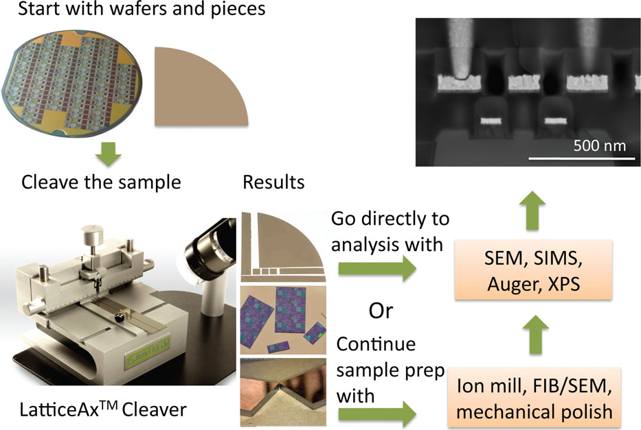
Figure 1: The workflow starts with a wafer or wafer piece that is cleaved using the LatticeAx™ cleaver. The sample can then go directly to the analytical tool or continue to the next sample preparation step.
Role of cleaving in the sample preparation workflow. Semiconductor samples are inspected either as a cross section or “top down.” Cross-section samples are needed to inspect subsurface features. As shown in Figure 1, if the original sample is a wafer or a die and a cross-section view is required, cleaving is typically the first step in the sample preparation procedure. In Figure 1, the LatticeAx cleaver was used to produce a cleaved sample for SEM and surface analysis. With sufficient targeting accuracy and quality, the sample can go directly into the analytical tool. The example results in Figure 1 show the clean cleaved edges. For critical dimension measurements, cleaved cross sections are preferred because they allow the image surface to be normal to the SEM electron beam. A SEM image of this type of sample is shown in Figure 1 (upper right) and is called a 90-degree cross section.
In the case where the top surface of the sample is of interest, sample preparation is straightforward. If a large-stage analytical instrument is available, the entire wafer can be analyzed without processing, or the wafer can be cleaved into smaller pieces for analytical tools with limited stage travel.
Advanced techniques such as FIB, automated polishing, and automated cleaving have benefits in terms of submicron—or in the case of FIB, nanometer—targeting accuracy, but the tradeoff is high cost, long cycle time, the need for skilled operators, and, in some cases, the presence of sample preparation artifacts [Reference Minor2]. When analyzing the sample preparation workflow, it often makes sense to insert a cleaving step that is fast and provides the accuracy and quality needed to either go directly to the analytical tool or to reduce the time using the tool for final preparation of the target.
Streamlining the workflow. The LatticeAx cleaver was developed to complement the existing tool set in the laboratory by streamlining the workflow. As shown in Figure 1, the LatticeAx can be inserted into the workflow in two key areas: (1) preparation of a sample for direct analysis, where it is essential to preserve the sample “as-is” without material loss, contamination, or modification, and (2) preparation of a sample for another preparation tool, where the most important requirement is to offer a fast step that improves the total cycle time and delivers better quality.
This LatticeAx process optimizes the very basic elements of the manual cleaving technique and overcomes manual cleaving disadvantages, such as lack of accuracy and repeatability. LatticeAx does this by integrating a high-magnification digital microscope and a fine-positioning mechanism to control the indent location and depth, as well as the cleaving operation. This machine-assisted hybrid cleaving tool bridges the gap between manual scribing and fully automated cleaving. It also increases success rates by any user while keeping costs down.
LatticeAx is fundamentally different from manual cleaving because it: (a) replaces human vision with a high-magnification USB digital microscope to precisely select the target at magnifications up to 80×, (b) replaces hand coordination with precision positioning knobs, resulting in a repeatable process that is not user-dependent, (c) produces an indent on the surface <1 mm in length, ~10 μm in width at a very shallow depth, (d) employs a controlled “slow cleave” that follows the crystal plane, rather than a breaking along a manually scribed line.
LatticeAx operation.Figure 2 shows the microscope and LatticeAx and the key components of the device. Figure 3 shows the digital microscope image and a selected target location (in black).
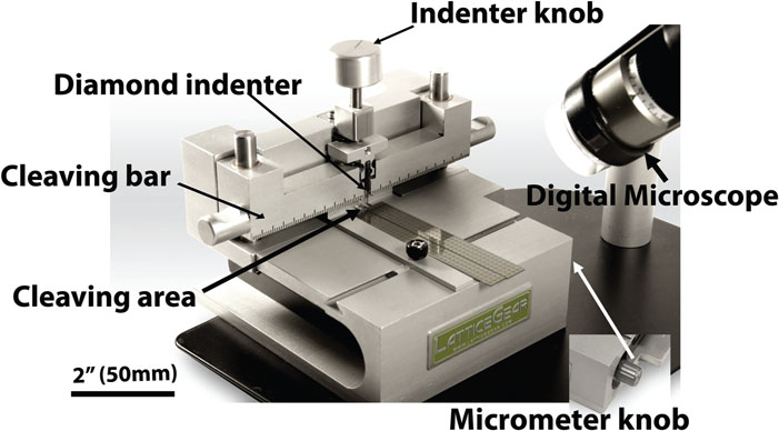
Figure 2: Key components of the LatticeAx.
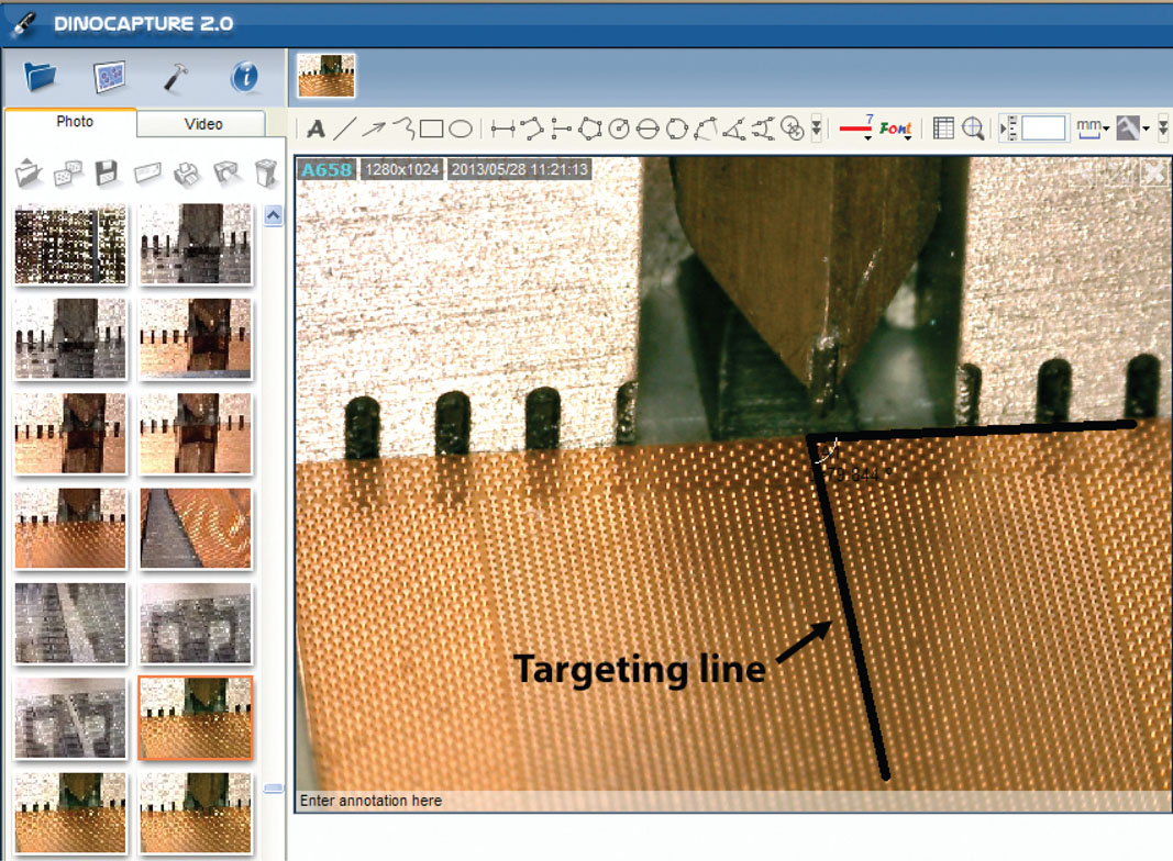
Figure 3: The LatticeAx software interface provides real-time video of the sample and cleaving area and graphical tools to align the indent to the target.
When cleaving with the LatticeAx, the workflow follows three simple steps: Set–Indent–Cleave (see Figure 4). Set: Set the sample on the plate and select the target; use the micrometer for fine positioning. Indent: Lower the diamond indenter with the indenter knob to make a fine indent at the edge of the sample. Cleave: Use the cleaving bar to apply uniform pressure over the fixed cleaving pin to achieve a controlled cleave along the crystal plane defined by the indent.
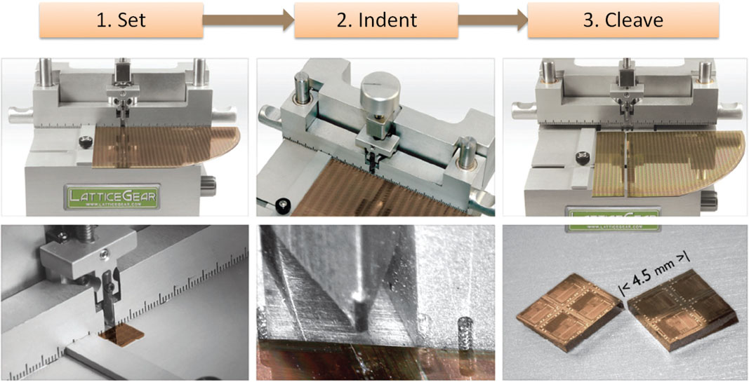
Figure 4: The LatticeAx process steps. Set: the target is selected using the digital microscope and the diamond indenter positioned. Indent: the precision control knob makes an indent at the edge of the sample. Cleave: this is performed by positioning the sample over the cleaving pin and applying uniform pressure with the cleaving bar.
Targeting is performed during the Set step. Using the software provided, the user draws a line that begins at the sample edge and extends through the target (Figure 3). The indenter is then positioned over the line using the micrometer (step size = 5 μm). Targeting accuracy to within 20 μm is achievable using a microscope magnification of 80×.
The best results are achieved when the indent is shallow, just penetrating the device structures. This very shallow indent makes an effective weak point in the silicon and results in a high-quality cross section when combined with the slow, 3-point cleaving. The slow cleave allows the time for the cleave to propagate along the crystal plane defined by the indent on the sample surface. In general, the larger the sample, the longer it will take to cleave.
Results
Case study 1: site-specific cleaving of etched TSVs. Through-Silicon-Vias (TSVs) bring connections from the front side of a wafer to the back side, where connections can be made to another 3D stack or to the package. One key step in TSV production is measurement of the TSV etch profile and the critical dimensions for process development and process control [Reference Teh, Caramto, Chidambaram, Wang, Arkalgud, Saito, Maruyama and Maekawa3]. Because TSVs can be up to 100 microns deep with aspect ratios of up to 1:20 or greater, cross-sectional examination in the SEM is the analysis method of choice.
The LatticeAx cleaver, now part of the SEM inspection workflow, provides the speed and accuracy needed for rapid development cycles. For this case study, SEMATECH 5 × 50 and 2 × 40 (diameter × depth, in microns) test structures were cleaved and inspected on the SEM.
Cross-section samples were prepared by cleaving the whole wafer into strips or pieces containing the area of interest, often a structure specifically included in the mask for the SEM (Figure 5a). The specific site was then cleaved using the LatticeAx, which has a targeting accuracy of 20 microns (Figure 5b).
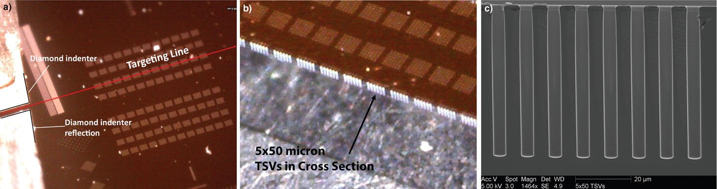
Figure 5: (a) During the Set step, the target is marked using the software's line function. (b) Optical image showing the cleaved edge of a 5 × 50 μm TSV test structure targeted in (b). (c) SEM image of a cluster of 5 × 50 μm test structures.
The process yields high-quality cross sections from the top to the bottom of the TSV (Figure 5c). The entire feature targeting and cleaving process was completed in 5 minutes. Once the cross section was prepared, it could be inserted in the SEM without further preparation.
Case study 2: flip chip solder bumps. Semiconductor manufacturers inspect solder bump reliability prior to dicing and packaging. The objective is to identify interconnect problems early in development or for the purpose of detecting electromigration failure. Fault isolation and physical failure analysis after packaging are time-consuming, require a high level of expertise, and can be costly, especially if the electronic devices have made it into the consumer market.
One method of inspection is performed by creating a cross section of the solder bumps and inspecting it for voids, cracks, intermetallics, or other abnormalities that could cause the device to be susceptible to failure immediately or after aging [Reference Oppert, Dohle, Franke and Haerter4].
The sample preparation procedure employed the LatticeAx and broad ion-beam milling to achieve high-quality SEM imaging for the analysis of failed devices and product reliability. The solder bumps were prepared for the SEM in a two-step process. In step 1, the LatticeAx cleaver was used to cleanly cross-section close to and parallel to a specific row of copper bumps. The copper bumps had a diameter of 85 μm and were cleaved 30 μm from the center of a bump. The time to cleave was 5 minutes and yielded the result shown in Figures 6a and 6b. In step 2, a broad, argon, ion-beam instrument, the Hitachi IM4000, was used to prepare the final imaging surface. The sample shown in Figure 6a was mounted topside down on a sample block to perform backside milling. Backside milling was used to prevent artifacts of ion beam milling that can occur as a result of sample topography [Reference Teh, Caramto, Chidambaram, Wang, Arkalgud, Saito, Maruyama and Maekawa3]. The ion milling process was performed at an acceleration voltage of 6 kV for 2 hours. By cleaving close to the center of the copper bumps, the time on the ion mill was minimized. No further preparation was performed.

Figure 6: (a) Before ion milling. As cleaved through a row of flip chip solder bumps (optical image). (b) SEM image before ion milling after cleaving with the LatticeAx to within 30 μm of the bump center. (c) SEM image after backside ion milling showing the milled trench and copper bumps. (d) SEM image after ion milling using the IM4000, showing all bumps intact and milled to the center of the bump. (e) Grain structure of copper bump and clear view of interface to copper interconnect and silicon. (f) Zoomed-in view of left edge of bump showing interface to copper and dielectric.
Figure 6c shows the direction of the ion beam during milling and the trench milled by the ion beam. Figures 6b and 6d show the solder bump cross section produced by the LatticeAx cleaver at the site of interest and after ion milling, respectively. Figures 6e and 6f, taken after ion milling, clearly show the copper grain structures and the fine details at the interface between the bump and adjacent structures.
This two-step sample preparation process creates artifact-free cross sections of copper solder bumps and the underlying interfaces and thin films.
Discussion
The LatticeAx can produce specimens directly for SEM analysis or it can be used as a first step in a multi-step preparation process. Applications for the LatticeAx, introduced to the market in November 2012, are still emerging. Interest is developing in the use of the LatticeAx to prepare samples for surface analysis tools such as SIMS, XPS, and Auger. Surface analysis requires ultra-high vacuum, and sample size is often limited to small x-y travel (1″), so it would be an advantage to be able to prepare samples of uniform size, with the target centered and without the creation of silicon dust or contamination.
Conclusion
Sample preparation is an important step in the characterization of semiconductor devices. This article presented the LatticeAx cleaver as a new addition to the sample preparation tool suite. It either stands alone as a preparation tool for the SEM or other analytical tool (case study 1) or can be introduced as the first step of the preparation process (case study 2). In both cases, this fills the need for a high-throughput, high-accuracy cleaving system that is cost-effective.
Acknowledgments
The authors would like to thank the support of SEMATECH's 3D Interconnect program for providing TSV samples and guidance on the analysis and interpretation of data.


