

Angstrom Science, Inc
Tel +1-805-845-7446
Email: info@angsci.com

Access™ Atomic Force Microscope (AFM)
APPLICATIONS: Combine AFM + Light Microscope • Fits on sample stage• All AFM techniques
FEATURES: Low Cost• Highest Sensitivity• Lowest noise of any AFM• Compact Design• Easy to use.

Bruker Nano Surfaces
Tel: 520-741-1044, ext. 1075
Email: Productinfo@bruker.com

Hysitron PI 88 SEM PicoIndenter
APPLICATIONS: In-Situ Mechanical Experiments for SEM • Targeted Nanoindentation with EBSD • Heating up to 800°C • Nanoscratch • Data-Video Correlation
FEATURES: Hysitron PI 88 is Bruker's comprehensive in-situ nanomechanical test instrument for SEM and FIB-SEM, enabling in-situ SPM imaging, nanoindentation, XPM accelerated property mapping, compression, tension, bending, and scratch tests in your SEM.
www.bruker.com/nanomechanical-testing

Hysitron PI 95 TEM PicoIndenter
APPLICATIONS: In-Situ Mechanical Experiments for TEM • Tensile Testing of Nanowires, Films, 2D Materials • Nanoscratch, Fatigue, Electrical, Heating • Data-Video Correlation
FEATURES: The only quantitative nanomechanical testing holder for TEM, enabling compression, tension, bending, scratch, and fatigue testing with simultaneous TEM observation of deformation behavior.
www.bruker.com/nanomechanical-testing

JPK NanoWizard 4 BioScience AFM
APPLICATIONS: BioAFM • Cell and Tissue Dynamics • Time-Lapse Studies on Molecules or Cells • Correlation with Optical Microscopy
FEATURES: NanoWizard 4 combines atomic resolution and fast scanning with rates up to 100 lines/sec and a large scan range of 100μm, all in one system.

Vutara 352 Super-Resolution Microscope
APPLICATIONS: Video-Rate, Single-Molecule Localization • Quantitative Super-Resolution Analysis • Correlative, High-Speed Confocal Imaging • Developmental Biology • Cardiology
FEATURES: Vutara 352's speed, imaging depth, and resolution deliver significant advantages over competing approaches, adding real-time quantitative analyses and including pair-correlation, co-location, cluster, and live-cell analysis.

Dimension XR SPM
APPLICATIONS: Quantitative Nanomechanical Analysis • Multi-Dimensional Nanoelectrical Characterization • Highest Resolution Scanning Electrochemical Imaging • Nanoscale Viscoelastic Analysis of Polymers
FEATURES: Packaged solutions for advanced, quantitative nanomechanical, nanoelectrical, and nanoelectrochemical research of materials and active nanoscale systems in air, fluid, electrical or chemically reactive environments.

Anasys nanoIR3 Spectrometer
APPLICATIONS: Hyperspectral NanoIR Spectroscopy Correlated to FTIR • Nanoscale Chemical Imaging • Complementary Tapping AFM-IR and s-SNOM 2D Materials Characterization • Semiconductor Failure Analysis
FEATURES: The nanoIR3 provides IR-based chemical imaging and mapping of chemical variations of sample. Point spectroscopy capabilities enable both spectroscopy and chemical imaging with a single source.

Ultima 2Pplus Multiphoton Microscope
APPLICATIONS: Neuroscience • Intravital Imaging • Optogenetics • Photoactivation and Photostimulation Experiments • In Vivo Imaging
FEATURES: Ultima 2Pplus delivers an ideal combination of flexibility, resolution, imaging depth and speed, allowing simultaneous imaging, stimulation and electrophysiology protocols with greater efficiency and effectivity.

ContourGT 3D Optical Microscope
APPLICATIONS: MEMS Characterization • Precision Machined Component Metrology • Tribology and Corrosion Analysis • High-Brightness LED Measurements • Opthalmic Characterization
FEATURES: The ContourGT utilizes over three decades of white light interferometric (WLI) innovation to deliver production-ready automation, measurement-angle flexibility, outstanding imaging, and proven gauge-capable surface metrology.

Bruker Nano Analytics
Tel: 1-800-234-9729
Email: info.bna@bruker.com

Electron Microscope Analyzers
APPLICATIONS: Energy-Dispersive X-ray Spectrometry (EDS) • Wavelength Dispersive X-ray Spectrometry (WDS) • Electron Backscatter Diffraction (EBSD) • Micro X-ray Fluorescence (Micro-XRF) on SEM • XFlash® Silicon Drift Detectors (SDD) for SEM and TEM
FEATURES: Bruker Nano Analytic's electron microscope analyzers QUANTAX EDS, QUANTAX WDS, QUANTAX EBSD and QUANTAX Micro-XRF on SEM offer unmatched comprehensive compositional and structural materials analysis.

Bruker Optics
Tel: (978) 439-9899
Email: info.bopt.us@bruker.com

LUMOS II FTIR Microscope
APPLICATIONS: Polymer Investigation • Surface Analysis • Particle Analysis • Pharmaceuticals • Life-Science • Forensics • Electronics • Automotive • Environmental

FEATURES: Incredibly fast FTIR imaging, where each pixel is composed of an entire FTIR spectrum. This results in superb spatial resolution and peak sensitivity in all measurement modes. Delivers the best performance in transmission, reflection and attenuated total reflection (ATR) measurements. Detect and immediately characterize tiny particles, product defects or tissue anomalies. Easily analyze any sample type of any origin.
Deben
Tel: +44 (0) 1359 244 970 & +1 (201) 962 7222
Email: paulg@deben.co.uk

In-situ testing for microscopy
APPLICATIONS: • Microtest tensile and compression stages • Micro CT tensile, compression and torsion stages • STEM & BSE detectors for SEM • Centaurus scintillator CL and backscattered electron (BSE) detectors • SEM heating and cooling Peltier stages

FEATURES: Deben manufactures in-situ testing stages as well as innovative accessories for SEM, Optical, AFM, XRD and X-ray tomography.
DECTRIS USA Inc.
Phone: +1.215.384.3479

DECTRIS QUADRO
APPLICATIONS: • Nanobeam electron diffraction • 3D precession electron crystallography • Strain mapping • STEM, 4D-STEM, Ptychography • In-situ imaging

FEATURES: The QUADRO detector is designed to deliver outstanding performances to materials science TEM without compromise on accuracy, speed, or sensitivity. Fully integrated into NanoMegas Topspin.
DECTRIS ELA
APPLICATIONS: Electron Energy Loss Spectroscopy • Elemental/chemical mapping • Atomic resolution STEM-EELS • Materials characterization

FEATURES: The ELA operates at 9000 spectra/sec in continuous readout mode. Elemental mapping runs in real time and momentum-resolved EELS can be done within minutes.
DiATOME U.S.
Tel: 215-412-8390
Email: info@emsdiasum.com; stacie@ems-secure.com

Cryo Immuno
APPLICATIONS: The first cryo knife with a diamond platform, guarantees the best possible sectioning for sucrose infiltrated samples (Tokuyasu).

FEATURES: The diamond platform guarantees an easy and gentle section pick-up. The sections are collected directly from the diamond surface using a loop and a sucrose/methyl-cellulose droplet.
EDAX Inc.
Tel: (201) 529-4880
Email: info.edax@ametek.com

Velocity™ EBSD Camera Series
APPLICATIONS: Scanning Electron Microscopes (SEMs) • Electron Backscatter Diffraction (EBSD) • Simultaneous Energy Dispersive Spectroscopy (EDS)-EBSD Collection • Lower Symmetry, Multi-Phase, or Deformed Structures • In-situ and 3D EBSD Applications

FEATURES: Powered by a CMOS sensor, the world's fastest EBSD camera combines high-speed acquisition with high sensitivity, low noise performance for optimal collection and data quality.
Electron Microscopy Sciences
Tel: 215-412-8400
E-mail: stacie@ems-secure.com

EMS-002 Cryo Workstation
The EMS-002 Cryo Workstation is a complete ultra rapid freezing system that captures rapid events and labile structures that are not seen in chemically fixed materials.

EMSIS GmbH
Tel: +49 251 297962-0 or -12
Email: info@emsis.eu

XAROSA 20 MP CMOS TEM Camera
APPLICATIONS: • All Life and Materials Sciences TEM imaging task • HR-TEM with speed and in-situ requirements • Diffraction imaging - no blooming to the CMOS sensor • Drift correction of drifting samples with no limitations • Capable of Low-dose and Cryo due to a perfect DQE
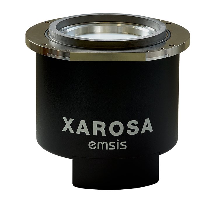
FEATURES: The XAROSA TEM camera features a 20 megapixel (MP) CMOS sensor with at least 30 frames per second (fps) in full 20 MP. A tapered fiber optics additionally provides a large field of view of 67 mm x 50 mm. In combination with its software RADIUS, the XAROSA offers drift correction, HDR imaging, smart averaging, “click-to-center” and many more features.
Evactron by XEI Scientific, Inc.
Tel: 650-369-0133
Email: sales@evactron.com

Evactron® E50 E-TC Plasma De-Contaminator
APPLICATIONS: In-situ hydrocarbon removal • SEM/FIB large chamber cleaning • TKD/EBSD sample optimization • SEM sample and TEM holder cleaning • Accurate nanostructure characterization

FEATURES: External hollow cathode 50 watt plasma source with touchpad control, fast cleaning/pumpdown of large chambers, “POP” ignition at high vacuum - no venting needed.
Evactron® TEM Wand
APPLICATIONS: Atomically thin 2-D materials • Nanoparticles and 1D materials • Atomic resolution imaging and chemical mapping • In-situ microscopy • Microstructure and mechanics deformation

FEATURES: Remove hydrocarbon contamination from JEOL TEM/STEM columns, 12 watt maximum power to clean sensitive objective lens surfaces, uses air to generate energy-efficient plasma.
https://evactron.com/evactron-tem-wand-plasma-de-contaminator/
Excelitas Technologies®
Tel: (+1) 800-775-6786
Email: generalinquiries.na@excelitas.com

X-Cite® Fluorescence Illumination Solutions
Email: x-cite@excelitas.com
APPLICATIONS: Digital Pathology or Virtual Microscopy • Fluorescence in Situ Hybridization (FISH) • Fluorescence Resonance Energy Transfer (FRET) • Live Cell Imaging • Optogenetics • Photoactivation

FEATURES: X-Cite offers innovative and reliable fluorescence illumination solutions for researchers and OEM integrators, with high power, control and stability required for their applications.
https://www.excelitas.com/product-category/x-cite-illuminators
Optem® FUSION Micro-Imaging System
Email: generalinquiries.na@excelitas.com
APPLICATIONS: Machine vision • Variable magnification imaging • Non-contact optical dimensional metrology • OEM integrated microscopy • Automated Optical Inspection

FEATURES: Optem Lenses feature interchangeable Mounting, Camera Tube, Optomechanical Function and Lower Magnification modules to enable users to configure their exact form, function and performance requirements.
https://www.excelitas.com/product/optem-fusion-micro-imaging-system
Mag.x System 125
Email: generalinquiries.na@excelitas.com
APPLICATIONS: Technical microscopy • Flat-panel display inspection • Semiconductor inspection & processing • Widefield biomedical imaging • Micro measurement & metrology • Scientifc R&D

FEATURES: The Mag.x System 125 represents a new class of optical systems that enables microscope-like resolution with wide fields-of-view supporting modern high resolution sensors up to 57 mm diameter.
https://www.excelitas.com/product-category/x-cite-illuminators
iFLEX Diode Lasers
Email: generalinquiries.na@excelitas.com
APPLICATIONS: Confocal microscopy • Optogenetics • Flow cytometry • Test & measurement • Biomedical imaging & instrumentation

FEATURES: iFLEX Lasers deliver exceptional power stability with low amplitude noise. kineFLEX™ fiber delivery options ensure stable intensity with sub-micron positional accuracy and streamlined system integration.
EXpressLO LLC
Tel: +1-321-663-3806
Email: info@EXpressLO.com

Nicola G2/G2F ex situ lift out and micromanipulator system
APPLICATIONS: • ex situ lift out • micromanipulation • particles, fibers, thin films • backside or plan view manipulation • FIB/SEM/TEM specimen preparation

FEATURES: EXpressLO™ grids and methods allow fast, easy, and flexible manipulation of FIB lift out specimens, fibers, particles, thin films, CNTs, and more.
Praxis™ 3D Printed Samples
APPLICATIONS • ex situ lift out • in situ lift out • manipulation practice and training • reduce FIB costs for sample preparation • access to many samples • easier and faster for more repetition

FEATURES: The patented Praxis™ 3D Printed specimens can be used for EXLO, EXpressLO™ or INLO methods, for training, practice, and educational purposes.
Gamma Scientific
Tel: +1 858-279-8034

APPLICATIONS: • Fluorescence Excitation • Spectrum/Illuminant Simulation • Camera and Image Sensor Calibration • Photodiode Detector Responsivity • Diagnostic Medical Imaging

FEATURES: The latest in tunable LED light sources, SpectralLED® products incorporate up to 35 discrete wavelengths for synthesis of unlimited spectral profiles from 380-1000 nm.
ibss Group, Inc.
Tel: +1-650-513-1488
Email: admin@ibssgroup.com

GV10x Downstream Asher
APPLICATIONS: • In-situ contamination control • Long MFP plasma cleaning • FIB/SEM, SIMS, XPS, TEM, CDSEMs, Review SEMs

FEATURES: High to low power pressure (<5e−3 Torr, 6.7e−3 mBar, 6.7e−1 Pascal), long mean free path plasma for cleaning chambers and specimens in-situ. User operation via ibss Controller and/or Windows PC
Mobile Cubic Asher
APPLICATIONS: In-situ & Ex-situ contamination control • SEM/FIB/TEM/SIMS/XPS • Sample Cleaning • Storage

FEATURES: Mobile downstream plasma cleaning center for specimen & in-situ EM cleaning, employs ibss signature GV10x Qwk-Switch source operated via touchscreen panel, fitted into one convenient enclosure.
Chiaro
APPLICATIONS: In-situ & Ex-situ contamination control • SEM/FIB/TEM/SIMS/XPS • Sample Cleaning • TEM holder view & storage

FEATURES: View / store TEM holders using gas and liquid samples, the Chiaro performs functions of leak check, E-Chips, hydrophilize sample surfaces and plasma cleaning.
International Centre for Diffraction Data
Tel: 610-325-9814
Email: info@icdd.com

Powder Diffraction File
APPLICATIONS: X-ray Powder Diffraction • Database • Software • Electron Diffraction • Education

FEATURES: The Powder Diffraction File™ (PDF®) is a collection of single-phase X-ray powder diffraction patterns for rapid phase identification designed to support automated quantitative analyses.
IXRF Systems
Tel: 512-386-6100
Email: info@ixrfsystems.com

EDS System
APPLICATIONS: SEM • Microanalysis • Trace Elements • Feature Analysis • EDS/XRF

FEATURES: Our EDS Microanalysis for the SEM is the most flexible EDS system you will ever use. Iridium Ultra will change the way you analyze data.
ATLAS Micro-XRF
APPLICATIONS: Microanalysis • Trace Elements • Thin Film • Large Area Stage Mapping • Micro-XRF

FEATURES: The ATLAS Micro-XRF spectrometer boasts the largest chamber volume and SDD detection area as well as the smallest XRF spot size available on the market.
LatticeGear LLC

“Dry Dicing” Surface Touchless Cleaving Tools
APPLICATIONS: Substrate downsizing • Device Singulation • Cross-sectioning

FEATURES: Our cleaving tools are cleanroom compatible and can be used for substrate material of any thickness and size, including glass, sapphire, III-V, SiC, and silicon.
Kammrath and Weiss
Tel: (516) 313-9742
Email: Sales@kammrathandweiss.com
https://www.kammrath-weiss.com/en/

In-Situ Tensile/Compression module
APPLICATIONS: Materials Science, Mechanical Engineering, Failure Analysis, Product Development

FEATURES: Vacuum and Benchtop compatible, compact for In-Situ SEM/FIB operation, Micro Newton to 10k Newton range with exchangeable load cells, single-axis or Bi-axial models
https://www.kammrath-weiss.com/en/products/materials/tensile-compression.html
Transfer module
APPLICATIONS: Materials Science, Mechanical Engineering, Failure Analysis, Product Development

FEATURES: Transfer sensitive samples from glovebox to vacuum chamber, Vacuum compatible, SEM/FIB compatible, Heating and cooling options
https://www.kammrath-weiss.com/en/products/materials/transfer-module.html
Linkam Scientific Instruments
Tel: +44 (0) 1737 363 476
Email: duncanstacey@linkam.co.uk

MFS Modular Force Stage
APPLICATIONS: Ideal for tensile and compression testing of polymers, rubbers, composites and other materials • Optional temperature control from -195°C to + 350 °C • Versions available that are compatible with FT-IR and Raman microscopes and spectrometers as well as X-ray systems. • Optional liquid cell for bio samples • Tensile, compression and 3-point bending testing – ranges from 0 to 2N up to 200N and higher

FEATURES: The new MFS has a modular design which can be configured to meet the needs of many tensile, compression or bending applications.
CMS196V3 Cryo CLEM Stage
APPLICATIONS: • Self-contained cryo correlative system avoiding contamination with automated liquid nitrogen refilling • High precision encoded motorized XY with high speed automated mapping • Short start up time with high long-term stability and low drift • Self-aligning magnetic sample cassette system for up to three EM grids • Integrated condenser optics for transmitted light

FEATURES: The Linkam Cryo-CLEM stage allows vitrified samples to be imaged in brightfield and fluorescence without contamination. Grids can be mapped to provide correlative information.
Optical DSC450 Stage
APPLICATIONS: • Differential Scanning Calorimetry from -150°C to + 450 with liquid nitrogen cooling • Optimized for simultaneous high-quality image capture and recording • Heating and cooling rates from 0.1°C/min to 30°C/min • Ideal for measuring glass transitions and melting peaks • Highly sensitive at low heating rates and small samples

FEATURES: The Optical DSC450 system is optimized to measure transition temperatures and enthalpy changes, while simultaneously being able to image the sample providing correlative information of physical changes such as morphology and colour.
RH95 Humidity Generator
APPLICATIONS: • Fully self-contained humidity control from 5% to 90%RH, no dry air supply required • Highly stable +/-0.5% making it ideal for long term material testing • Compatible with a range of Linkam stages and other sealed chambers up to 2 liters • Optional accessory for use of Nitrogen carrier gas • Optional calibration kit including chamber and salt ampoules

FEATURES: The RH95 Humidity Generator provides precise control of RH% for a range of Linkam stages. Ideal for sample characterization under changing environmental conditions.
THMS600 Heating and Cooling Stage
APPLICATIONS: • -195°C to + 600°C temperature range with optional liquid nitrogen controller • Heating rates up to 150°C/min; cooling rates to 100°C/min • Better than 0.01°C temperature accuracy and resolution • Options for gas control, humidity, pressure, vacuum and electrical measurements • Versions available that are compatible with FT-IR and Raman microscopes and spectrometers as well as X-ray systems.

FEATURES: The most versatile heating and cooling stage available. Precise and accurate temperature control ideal for use with light microscopy, FT-IR, UV, Raman, X-Ray, SAXS/WAXS and Synchrotrons.
Mad City Labs Inc.
Tel: +1 608 298-0855
Email: sales@madcitylabs.com

Nanopositioners, AFM, NSOM, Single Molecule Microscopes, Modular Microscopy
APPLICATIONS: Piezo nanopositioners for sample scanning and objective lens movement • Atomic Force Microscopy (AFM) • Near Field Scanning Optical Microscopy (NSOM) • Single Molecule Fluorescence Microscopy • MicroMirror TIRF and Super Resolution Microscopy

FEATURES: Closed loop nanopositioners with proprietary high stability PicoQ® sensors. Designed for nanoscopy and microscopy applications. Unique MicroMirror TIRF single molecule microscope. Low cost AFM and NSOM with flexible configurations.
Microscopy Innovations
Tel: (715) 384-3292
Email: Info@microscopyinnovations.com

ASP-1000 Automated Specimen Processor
APPLICATIONS: Biological TEM specimen prep • Serial block-face EM (3DEM) • Immunogold labeling (pre- or post-embedding) • Automated tissue processing • Customized workflows

FEATURES: ASP-1000 provides load-and-go convenience, one-touch specimen handling through resin-infiltration, batch-to-batch consistency/reproducibility, simple set-up/clean-up, and accelerated processing (e.g., 46-minute kidney prep) for increased throughput.
Microtome Service Company
Tel: 315-451-1404
Email: Microtome.Svc.Co@verizon.net
http://www.microtomeserviceco.com

Microtome Sales, Service and Parts
APPLICATIONS: • Sorvall Microtomes and Ultramicrotomes • Rotory Microtome Repair • KnifeMaker Repairs • AO 820 & AO 860 Repairs • Fabricate & Modify Lab Equipment

FEATURES: Sales & Service of Sorvall, RMC, AO:820, 860 and Rotary Microtomes and GKM Knife Makers. Microtome & Lab accessories, fabrication and modifications to meet your specific needs. Microtome Rentals.
http://microtomeserviceco.com/index.php?route=information/information&information_id=7
Minitool Inc.
Tel: (408) 395-1585
Email: rschaller@minitoolinc.com

Microtools and Instruments
APPLICATIONS: • Microscopy • Microbiology • Specimen Manipulation & Placement • Medical Research • Spectroscopy

FEATURES: Efficient, precise and realistically proportioned instruments in tip diameters from .025mm (.001″) to 1.0mm (.040″) are ideal for microscopists. Our line of micro-tools includes needles, gravers, chisels, knives, mirrors, probers, spatulas, hooks, scribes and microrulers. Also featured are micromanipulators, micro-sharpeners and micro-forceps. Tools are offered singly or in sets of eight tools with one handle to 32 tools with six handles.
Navitar
Tel: 585-359-4000
Email: info@navitar.com

Zoom 6000 Gen 2.0
APPLICATIONS: Vision • Medical Imaging • Microscopy • Inspection • Metrology
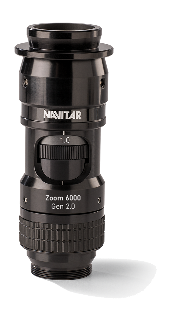
FEATURES: Navitar's Zoom 6000 Gen 2.0 is optically redesigned and an improved upgrade to our legacy Zoom 6000 with same quality, life cycle performance and attention to detail. The system is both backwards compatible and future proof.
https://navitar.com/products/imaging-optics/high-magnification-imaging/
Olympus Scientific Solutions
Tel: (281) 922-9300
Email: info@olympus-ossa.com

LEXT® OLS5000 3D Laser Confocal Scanning Microscope
APPLICATIONS: • Non-contact 3D surface metrology • 3D Imaging • Nanofabrication • MEMS • Failure Analysis

FEATURES: Olympus’ LEXT OLS5000 laser scanning confocal microscope features 4K scanning and dedicated objectives for measurements on 210 mm samples and concavities up to 25 mm.
Oregon Physics
Tel: +1 503 601 0041
Email: info@oregon-physics.com

Hyperion II Dual Polarity Ion Source
APPLICATIONS: Negative and positive ion extraction • Bolt-on to existing optical system • Utilize variety of gas species • Supports surface analysis (SIMS) applications • Supports high current micromachining (PFIB) applications

FEATURES: Integrates on existing ion optical systems to deliver the highest brightness, best imaging resolution and longest source lifetime for SIMS applications or high current FIB.
FIB Consumable Parts
APPLICATIONS: For FEI FIB columns • Suppressors • Extractors • Custom aperture strips • Standard aperture strips

FEATURES: High quality FIB replacement parts for FEI brand DualBeam and FIB systems at substantial cost savings. We offer fast delivery and discounts for volume orders.
Park Systems
Tel: 408-986-1110
Email: inquiry@parksystems.com

Park NX 12- Park NX12 features a versatile Inverted Optical Microscope (IOM) based SPM platform for SICM, SECM, and SECCM, in addition to Atomic Force Microscopy for research on a broad range of materials from organic to inorganic, transparent to opaque, soft to hard.
FEATURES: • Atomic Force Microscopy (AFM) for nanometer resolution imaging with electrical, magnetic, thermal, and mechanical property measurement capabilities • Pipette-based scanning system for high resolution Scanning Ion Conductance Microscopy (SICM), Scanning Electrochemical Microscopy (SECM), and Scanning Electrochemical Cell Microscopy (SECCM) • Inverted Optical Microscopy (IOM) for transparent material research and fluorescence microscopy integration
APPLICATIONS: Park NX12- Park NX12 was built from the ground up to accommodate the needs of multi-user facilities. Other AFM solutions lack the required versatility to address the diverse needs of users in these facilities, making it difficult to justify the equipment cost. The Park NX12, however, is built to accommodate standard ambient AFM, in-liquid SPM and optical imaging making it one of the most flexible AFMs available.
https://www.parksystems.com/index.php/products/small-sample-afm/park-nx12/technical-info
PI (Physik Instrumente) LP
Tel: 508-832-3456
Email: info@pi-usa.us

PInano® Nanopositioning Solutions for Light-Sheet & Super-Resolution Microscopy
APPLICATIONS: Super Resolution Microscopy • Microscopy Stages • Atomic Force Microscopes (AFMs) • Positioning Stages & Controllers • Nanopositioners & Stages

FEATURES: 2nd Gen System • Two Versions: High Precision / High Precision and Stability • Cost-effective Piezoresistive Feedback Version Available • Extremely Fast Step & Settle, From 5msec • Low Profile: 20mm (0.8″) • 200μm Travel Ranges
SCHOTT North America, Inc. – Lighting and Imaging
Tel: +1-508-765-9744
Email: lightingimaging@us.schott.com

Fiber optic & direct LED illumination for microscopy applications
APPLICATIONS: Stereo Microscopy • Laboratory Equipment • Industrial Applications • Life Science Applications • Microscopy Applications

FEATURES: We offer a complete portfolio in Fiber Optic and direct LED illumination for stereo microscopy to provide the most suitable contrasting solution for a variety of applications.
https://www.us.schott.com/lightingimaging/english/microscopy/products.html#block380557
Cold Vision Series – Ruggedized Halogen and LED Light Sources & Accessories
APPLICATIONS: • Stereo Microscopy • Laboratory Equipment • Industrial Applications • Machine Vision Applications • Microscopy Applications

FEATURES: Built also for heavy duty environments, the Cold Vision series offers in a ruggedized housing modular fiber optic illumination with an extensive range of light guides and accessories.
https://www.us.schott.com/lightingimaging/english/microscopy/products.html#block362623
Pixelink
Tel: 1-833-247-1211
Email: sales@pixelink.com

Industrial 10 GigE Cameras
APPLICATIONS: Automated inspection • sports analysis • 3D mapping • research • VT and AR applications

FEATURES: Pixelink's new high performing PL-X machine vision camera series with 10 GigE interface gives you speed, accuracy and reliability in a quick and easy set-up.
https://pixelink.com/products/industrial-cameras/10-gige-cameras/
Special Optics
Tel: 973.366.7289
Email: sales@specialoptics.com

Custom Microscope Objectives
APPLICATIONS: Lifesciences, Defense and Security, Metrology, Medical Diagnostics, Laser Eye Surgery

FEATURES: We specialize in the design and manufacture of custom microscope objective lenses for researchers and OEMs who require a solution to a complex application that cannot be solved by off-the-shelf microscope objective lenses.
https://specialoptics.com/products/microscope-objectives/objectives/
SPI Supplies
Tel: 610-436-5400
Email: sales@2spi.com
URL: www.2spi.com
UV Prep
APPLICATIONS: Materials Science • Life Science • Semiconductor • Low Voltage Imaging • High Resolution SEM

FEATURES: The UV Prep is designed to remove hydrocarbon contamination from a sample surface prior to FE-SEM examination. The result is enhanced imaging and resolution at low accelerating voltages.
Plasma Prep™ III
APPLICATION: •Materials Science •Life Science •Semiconductor •Asbestos •Failure Analysis

FEATURE: Solid state RF generator capable of 1 to 100W operations; Low Temperature asher/etcher; small footprint; 4″ diameter x 6″ depth Pyrex or Quartz Chamber; Optional Process Controller; Optional system for cleaning TEM Specimen Holders.
Wet Cell II
APPLICATIONS: •Materials Science •Life Science •Microfluidic Analytical Techniques •Self-contained Interface • SEM

FEATURES: The next generation device for the examination of liquids in SEM/EDS and TOF-SIMS instruments. The self-contained high vacuum compatible device enables the analyst to characterize a fluid in its natural state.
Sputter/Carbon Coaters for SEM
APPLICATIONS: •Materials Science •Semiconductor • Imaging •Failure Analysis

FEATURES: The SPI-Module line of modular sputter coaters and carbon coaters are optimized for precious metal coating and/or carbon coating for all SEM/EDS applications.

BOB - Open-Design Upright Microscope
APPLICATIONS: Fluorescence microscope • In vivo and in vitro microscopy • Life and Material Sciences • Photostimulation

FEATURES: The BOB is a compact, height-adjustable microscope that can be easily configured to different types of experiments, methods of illumination and means of signal detection.
Ted Pella, Inc.
Tel: 800-237-3526
Email: sales@tedpella.com

High Resolution FE-SEM Sputter and Carbon Coaters
APPLICATIONS: • Life Sciences • Materials Science • Semiconductors • SEM

FEATURES: • Fine-grained, ultra-thin uniform and conformal coating • Wide choice of operating parameters to accommodate all sample types • Purpose designed with optimized vacuum pumping system • Rotary-Planetary-Tilting stage and high resolution thickness controller • Easy to operate with fast cycle times
NEW PELCO BioWave® Pro+
APPLICATIONS: • Microwave Tissue Processing for EM • Light Microscopy • Immunolabeling and Decalcification

FEATURES: User-friendly run screens with live run-time graph • Simplified protocol selection • Report Protocol Manager App and two USB ports for simplified data transfer and custom protocol upload
www.tedpella.com/microwave_html/pelco-biowave-pro-plus-microwave-system.htm
PELCO® Dimpler™
APPLICATIONS: Materials Science • Semiconductor Failure Analysis • TEM

FEATURES: Precision specimen thinning to near electron transparency at the exact region of interest, increased productivity for thinning compared to ion milling alone, automated operation for ease of use
PELCO® Tripod Polisher™
APPLICATIONS: Materials Science • Semiconductor Failure Analysis • TEM • SEM

FEATURES: Simple hand-held precision specimen preparation tool for thinning parallel to plane or angled to plane (wedge polishing) for thinning down to a region of interest or for electron transparency at the wedge tip, is easily used on any rotating metallographic grinder/polisher that has clear access to the platen surface.
www.tedpella.com/Material-Sciences_html/PELCO-Tripod-Polisher-590.htm
PELCO® Precision Lapping Fixtures
APPLICATIONS: Precision low deformation cutting of a wide variety of specimen types

FEATURES: PELCO® Lapping Fixtures allow for lapping of samples from <1/8” (3mm) to 1” (25mm) in diameter, and up to 1/2” (13 mm) thick. Micrometer and shim-controlled versions are available. Fixtures are equipped with tungsten carbide feet, which are highly resistant to wear from the lapping process.
www.tedpella.com/Material-Sciences_html/PELCO-Precision-Lapping-Fixtures.htm
PELCO® Precision Low Speed Saw
APPLICATIONS: Compact • multipurpose • low-damage cutting for all specimen types

FEATURES: Its low speed makes it possible to cut fragile materials that would otherwise fracture as well as soft materials that would load the diamond wheel on a higher speed saw. A variety of sample holders are available, providing a means for mounting any shape of sample.
www.tedpella.com/Material-Sciences_html/PELCO-Precision-Lapping-Fixtures.htm
Metallographic Consumables
APPLICATIONS: Materials Science, Metallography, Petrography, Semiconductor Failure Analysis

FEATURES: Wide selection, good quality, affordable prices.
www.tedpella.com/Material-Sciences_html/metallography-overview.htm
PELCO easiGlow™
APPLICATIONS: • Life Sciences • Materials Science • TEM • Tomography

FEATURES: Precise and easy vacuum settings • Short cycle times • Consistent results • Intuitive touch screen for control and display • Supports hydrophilic/hydrophobic and negative/positive modes
PELCO® Silicon Nitride Support Films and TEM Supplies
APPLICATIONS: • TEM • STEM • Thin Film Research • Life Sciences • Materials Science

FEATURES: Holey SiN films down to 100nm • Solid membrane thickness of 8, 15, 35, 50 and 200nm • 3mm diameter frame fits standard TEM holders • EasyGrip™ edges for improved handling • Variety of window shapes and sizes
PELCO® Modular SEM/FIB Sample Holders and Supplies
APPLICATIONS: • SEM • FE-SEM • FIB • FIB/SEM • CLEM

FEATURES: Stage adapters for all major SEM brands • Large selection of effective and practical sample holders • Correlative microscopy sample holders • Conductive adhesives • Carbon tabs • Conductive tape
Optical Light Microscopy & SEM Calibration Standards
APPLICATIONS: Calibration Specimens for SEM, TEM, AFM • SPM, FIB, EDS • WDS and Optical Microscopes


FEATURES: X-Ray References Calibration for SEM: PELCO X-CHECKER™ • Pelcotec™ CDMS-XY: Critical Dimension Magnification Standards • AFM Gold Calibration Kit • AFM TipChecker • Magnification Calibration Calculators • Pelcotec™ LMS-20 G Magnification Calibration Standard • Stage Micrometers • Fluorescence Reference Slides
TESCAN USA Inc.
Tel: 724-772-7433
Email: info@tescan-usa.com

TESCAN CLARA
APPLICATIONS: Routine study and industrial inspection of metal samples at the nanoscale • Routine imaging of nanoparticles and agglomerates of all kinds • Analysis of beam sensitive and non-conductive materials • Analysis of plants, micro-organisms and other biological specimens • Morphological and elemental characterization of geological samples

FEATURES: Unique In-Beam BSE detector designs allow filtering of signal based on energy and take off angle • Excellent for imaging of beam-sensitive and non-conductive samples • Fast setup of electron beam – optimal imaging and analytical conditions guaranteed • UHR Field-free characterization of materials at low beam energies for maximum topography • Intuitive and precise live SEM navigation on the sample at low magnification without the need of optical navigation camera • Intuitive Essence™ software modular platform designed for effortless operation regardless of the user's skill level
https://www.tescan.com/product/sem-for-materials-science-tescan-clara/
TESCAN SOLARIS
APPLICATIONS: TESCAN SOLARIS is a turn-key FIB-SEM solution for the fabrication of nanostructures and nanotechnology-inspired microscale functional devices. TESCAN SOLARIS combines the most precise Focused Ion Beam with UHR-SEM featuring TriLens™ immersion optics, to ensure the best possible connection between ion beam milling and ultra-high-resolution SEM imaging

FEATURES: Best-in-class ion beam performance • Crossover-free ultra-high resolution SEM imaging • High precision nanopatterning engine for electron and ion beams • Multiple gas injection system options with a variety of precursor gases • Chamber extension options for up to 12” wafer inspection • Easy-to-use modular software user interface • Python scripting interface for advanced user-defined experiments
https://www.tescan.com/product/fib-sem-for-semiconductors-tescan-solaris/
TESCAN AMBER
APPLICATIONS: A field-free UHR-SEM combined with the most precise FIB for sample preparation, sub-surface and 3D analysis capabilities to take your materials nanocharacterization further

FEATURES: Ultra-high resolution field-free SEM imaging and nanoanalysis • The highest precision micro sample preparation • Excellent low-keV ion beam performance • Multi-site FIB process automation • Multimodal FIB-SEM nanotomography • Extended field of view and easy navigation • Easy-to-use modular software interface
https://www.tescan.com/product/fib-sem-for-materials-science-tescan-amber/
TESCAN AMBER X
APPLICATIONS: A unique combination of Plasma FIB and field-free UHR FE-SEM for multiscale materials characterization • Optimized plasma FIB-SEM platform for high-quality deprocessing of the most modern semiconductor devices with proprietary chemistries • Milling and polishing of large cross sections • Multiscale, multi-modal FIB-SEM tomography •

FEATURES: High throughput large area FIB processing • Ga-free microsample preparation • Field-free ultra high resolution low energy electron beam imaging • In-beam SE and BSE detection • Optimized e-beam performance for high-throughput, multi-modal FIB-SEM tomography • Superior field of view for easy navigation
https://www.tescan.com/product/fib-sem-for-semiconductors-tescan-amber-x/
TESCAN DynaTOM
APPLICATIONS: The world‘s first dedicated dynamic micro-CT for your in-situ experimental needs • Multi-phase fluid flow in porous media • Tensile failure studies of structural alloys and composite materials • Crack propagation and fracture mechanics in engineered materials, geological samples and more • Hydration studies in porous materials from geoscience to consumer products • Crystal growth and mineralization in geo materials and construction materials • Plant germination, growth and decay • Freezing, melting and heating cycles in food science applications

FEATURES: Imaging of Delicate Samples • Gantry-based Design • Continuous Scanning • High Throughput • Unique Software Tools for 4D • Dynamic Screening for Synchrotron Beamtime • Acquila, a modular software architecture for tomographic acquisition and 3D reconstruction
https://www.tescan.com/product/micro-ct-for-materials-science-tescan-dynatom/
Thermo Fisher Scientific
Email: info.spectroscopy@thermofisher.com
thermofisher.com/microanalysis

Pathfinder Microanalysis Platform
APPLICATIONS: • Energy-dispersive X-Ray spectroscopy (EDS) • Wavelength-dispersive X-ray spectroscopy (WDS) • Electron Backscatter Diffraction (EBSD) • Silicon Drift Detectors (SDD) • High throughput, accurate elemental analysis

FEATURES: Pathfinder provides highly accurate EDS & WDS quantification with high sensitivity EBSD for both routine and advanced analysis of the most challenging samples.
UQG (Optics) Ltd
Tel: +44(0)1223 420329
Email: Sales@uqgoptics.com

Microscope slides, Coverslips & Optical Components
APPLICATIONS: Microscopes • UV-VIS Spectroscopy • Camera Windows • OEM Instrumentation • Viewing Windows

FEATURES: Fused Quartz and UV Fused Silica laboratory glasses, Technical glasses and OEM optics for instrumentation for the UV-Vis-IR for UV confocal, microscopy and research instruments.
