Introduction
Low-loss electron (LLE) imaging in the scanning electron microscope (SEM) is based on the collection of energy-filtered backscattered electrons (BSE) that have undergone minimal elastic interactions within a sample and therefore can carry high-resolution, surface-specific information. The earliest known record of the LLE technique was its introduction in a 1971 Applied Physics Letters communication authored by Oliver C. Wells [Reference Wells3]. That LLE paper followed a communication the previous year [Reference Wells4] describing the contrast mechanisms of BSEs collected at various take-off angles. Wells put the concepts presented in the 1970 paper together with a statement he credited to McMullan from 1953, that the signal collected in the SEM could be “…..restricted to the electrons which have lost only small amounts of energy and which have therefore travelled only short distances through the specimen” [Reference McMullan5]. Therefore, LLE collection likely evolved from those two concepts. Wells and his co-workers carried LLE forward to become a viable imaging technique; they developed the theory and fabricated a working LLE detector capable of demonstrating that concept. For many years, Wells researched and refined the LLE technique to fulfil his vision of collecting the highest-resolution surface information possible from the SEM. He also promoted LLE imaging to the scientific community and many of the instrument manufacturers (Figure 1).

Figure 1 Oliver C. Wells presenting a talk on the backscattered electron image.
Discussion
Image resolution
Oliver Wells described the LLE technique extensively in a number of publications [Reference Wells6–Reference Wells11]. During this work, Wells not only successfully imaged many conducting materials, but also non-conducting samples such as uncoated photoresist at high and low electron landing energies/accelerating voltages [Reference Wells and Richton12–Reference Wells16]. This work not only demonstrated that the LLE imaging revealed excellent surface detail, but also demonstrated that the effects of specimen charging could be mitigated (but not eliminated) when working with the conventional BSE or LLE imaging modes (Figure 2). In addition, Wells calculated the depth of signal generation, which is critical to understanding the origin of the collected signal. His calculations revealed that under the operating conditions they were using, while observing an uncoated magnetic recording head, the 500 eV energy window, resulted in about a 7 nm information depth. It was stated, in that paper, that the depth could be reduced to ~1 nm if the energy window were reduced to ~20 eV [Reference Wells13].
Figure 2 Comparison of the secondary (left) and LLE images (right). Reproduced with permission from the Microbeam Analysis Society, 1987 [Reference Wells15].
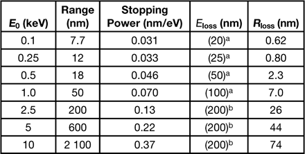
LLE detector
A diagrammatic representation of the LLE detector is shown in Figure 3. The heart of the detector is a retarding field energy filter, which is used to obtain the required energy resolution while subtending an adequate solid angle to the surface of the specimen. Wells stated [Reference Wells13] that an Eloss = 0.1xEinitial or 20 eV whichever is larger (at low landing energies) is a limit for this imaging. In practice the low-loss image works best if Eloss is no greater than ~ 200–300 eV as shown in Table 1, reproduced from that 1986 paper [Reference Wells13].
Figure 3 Schematic of the original design for the LLE detector. Reproduced with permission from AIP Publishing LLC, copyright 1971 [Reference Wells3].
Table 1 Calculated values for the average penetration distance Rloss needed to lose the stated energy loss Eloss Reproduced with permission from AIP Publishing LLC, copyright 1986 [13].
a E loss = 0.1 xE 0 or 20 eV, whichever is larger.
b In practice, the low-loss image works best if E loss is no greater than ~200-300 eV.
In-Line critical dimension metrology
The early LLE work only touched on the advantages afforded by LLE as applied to non-destructive low electron landing energy applications [Reference Wells and Richton12–Reference Wells16]. This early work did not fully explore the low landing energy techniques then just beginning to be employed in semiconductor metrology for process control nor its potential for non-destructive in-line metrology. Poor signal-to-noise and instrument limitations were significant issues, which were difficult to overcome with the class of instrumentation available at that time. However, the results were extraordinary. As shown in Figure 2, there is a significant improvement in the information content available in the LLE images relative to the conventional secondary electron (SE) images for the materials observed and under the instrument conditions used. However, today high-resolution field emission instrumentation coupled with charge balance techniques can generally permit successful imaging by varying instrument conditions beyond those available at that time.
Typically, on-line semiconductor metrology instruments used (and still use) the SE image for metrology because that signal mode is much stronger and typically provides a much better signal-to-noise ratio than either conventional BSE or LLE signals. In the throughput-driven world of semiconductor manufacturing, these decisions, and the choice of signal, were mediated by the available instrument designs based on, in part, the tungsten and lanthanum hexaboride electron source instruments available and the conventional flat final lens and early conical lens designs. At that time, field emission and digital frame storage were just in their infancy, and in-lens detectors had not been fully developed. Hence, the LLE signal-to-noise ratio was typically poor at the low landing energies, and the SE signal was deemed a much better signal choice. LLE was relegated to the microscopy “back burner.”
Somewhat later, work at the National Institute of Standards and Technology (NIST) began to explore the possibility of using BSEs for dimensional metrology and standards development [Reference Postek17]. Electron beam interaction modeling was in its infancy by comparison with today’s capabilities. Even so, the BSE image presented the distinct advantage that it was able to be modeled with the computer code developed at that time by Joy [Reference Joy18–Reference Joy20] and others [Reference Radzimksi and Russ21–Reference Lowney23]. In that preliminary work, the conventional BSE signal was shown to be potentially useful at low landing energies using the Healey and Moll converted backscattered secondary electron (CBSE) detection technique [Reference Moll24, Reference Moll25, Reference Postek17] and later using a microchannel-plate electron detector [Reference Postek26]. The microchannel plate detector was useful because it could be used to collect both SEs and BSEs with the same detector geometry. Optimizing operating conditions in experiments comparing SE imaging versus BSE imaging showed that measurements done under similar conditions with BSEs report typically smaller (closer to reality) dimensions than the same structures measured with the SE image [Reference Postek27]. This difference was documented for semiconductor production, and depending on the sample and instrument conditions it could be significant. Additionally, collection and measurement of the BSE signal demonstrated higher overall measurement precision. The BSE mode of electron collection was successfully adopted for semiconductor production applications by one critical dimension scanning electron microscope (CD-SEM) manufacturer, until throughput issues became a limiting factor. The LLE image, in theory, was thought to be a highly advantageous route to take because the electron beam-interactions could be controlled, and the sample-to-detector geometries were able to be measured with a high degree of confidence.
NIST collaboration
In order to investigate the potential of the application of LLE imaging to semiconductor metrology, Oliver Wells initiated collaborative work between the NIST and IBM Corp to explore LLE for accurate dimensional standards development and semiconductor process control (Figure 4) [Reference Postek28, Reference Wells29]. The work undertaken at NIST sought to reduce some of the geometrical limitations by using an instrument with the (then) new in-lens detector designs. It also sought to improve the signal-to-noise ratio problems through the use of frame storage and a high-brightness field-emission electron gun. A major goal was to assess the capabilities for LLE imaging for accurate metrology at low accelerating voltages.
Figure 4 Samuel N. Jones of NIST and Oliver C. Wells preparing a sample for viewing on the modified specimen stage of the NIST high-resolution field emission SEM. The modified stage held both the LLE detector and the sample.
Success, but with a caveat
Overall, the collaborative metrology work successfully demonstrated that, given the proper geometries, the LLE signal does provide more surface-specific information, especially at low landing energies than the SE image, and that the LLE image may be able to be more readily modeled. LLE detection is possibly the best signal for accurate SEM–based dimensional metrology and 3-D surface imaging. However, it presents huge technical challenges. As implemented by Wells in the NIST instrument, the signal-to-noise ratio and geometric considerations remained less favorable than with the standard SE imaging method. Therefore, it was concluded that if accurate SEM metrology was desired utilizing this methodology, a properly designed, dedicated metrology tool based on LLE optimization would be necessary.
Proposed improvements
Wells foresaw the need for a dedicated instrument. He and his colleagues developed a magnetically filtered low-loss detector [Reference Wells10, Reference Hodgson30] located within the magnetic field of the condenser lens. Today, we are closer than ever to this goal. New SEM column designs with efficient in-lens electron detectors have facilitated the potential for a resurgence of the use of energy-filtered electron collection.
Conclusion
The value of LLE has not been fully exploited but has not been forgotten. Some of these early results coupled with further experimental and modeling work can continue the exploration into the possibilities that LLE affords to accurate metrology. Determination of information related to geometric and design parameters necessary for full implementation of this technique should fulfil Oliver Wells’s vision of collecting the highest-resolution surface information possible from the SEM.