


1. Introduction
With a wide direct band gap of 3.39 eV and excellent physical properties gallium nitride (GaN) is a very promising material for fabricating blue light emitting devices. A few possible applications are high density optical data storage, full colour video-screens and even traffic lights. Significant progress in epitaxial growth of GaN has already led to commercially available nitride-based high brightness light emitting diodes Reference Akasaki and Amano[1] Reference Nakamura, Senoh, Iwasa, Nagahama, Yamada and Mukai[2] and very recently the first GaN blue laser was announced Reference Nakamura, Senoh, Nagahama, Iwasa, Yamada, Matsushita, Kiyoku and Sugimoto[3]. In spite of this recent success the growth of GaN and its alloys remains a challenge.
High quality GaN has been grown by several epitaxial techniques, such as MOCVD and MBE. At the moment MOCVD seems to be the most successful and certainly the most promising for large scale production. Nakamura attributes his success in nitride research to the two flow reactor, which was designed especially for nitride growth Reference Nakamura, Harada and Seno[4]. However several reactor designs have been suggested to tackle the specific problems associated with GaN growth. In this paper the achievements in GaN deposition in a novel type of vertical rotating disk MOCVD reactor are demonstrated. The optimisation of growth parameters and the characterisation of GaN films is discussed.
2. Experiment
2.1 The MOCVD-reactor
GaN films were grown by metalorganic chemical vapour deposition on two inch sapphire (0001) substrates with a H2 and mixed H2/N2 carrier gas. Ammonia (NH3) and trimethylgallium (TMG) were used as source materials. The growth was conducted in a vertical rotating disk reactor, manufactured by Thomas Swan & Co (see Figure 1). The group III and group V elements are injected separately into the reactor through a water cooled “showerhead” to avoid undesired upstream pre-reactions. Because the “showerhead” consists of several hundred fine tubes, the gasses are introduced uniformly into the reactor. A graphite resistance heater is used to raise the temperature of a graphite susceptor up to 1200 °C. The temperature is measured with an optical pyrometer looking directly at the substrate or the susceptor (three positions are available to monitor the temperature profile during growth). The substrate is placed on a rotating susceptor to achieve an improved uniformity and lateral flow regime across the substrate surface. The rotation speed of the susceptor can be varied between 0 and 1500 rpm (typically 800 rpm). Deposition was performed under atmospheric pressure (700 Torr) and low pressure (70 Torr).

Figure 1. Novel type of vertical rotating disk reactor.
2.2 Growth procedure
The substrates were degreased in organic solvents (Trichlorethane, Acetone, IsoPropyl Alcohol) and etched in a hot (180 °C) solution of H2SO4:H3PO4(3:1). Before growth the substrates were baked out at 1060 °C in a hydrogen atmosphere. After the bakeout the substrate is flushed with NH3 to nitride the surface. The growth of GaN is performed as a two step process. In the first step a nucleation layer is grown at a low temperature in between 450 and 550 °C. Then the temperature of the substrate is raised to between 950 and 1100 °C and kept constant for several minutes. During the annealing the nucleation layer recrystallizes and on this improved nucleation surface the GaN epilayer is deposited. Standard flow rates for carrier, NH3and TMG were 4 l/min, 2.5 l/min and 29 μmol/min respectively. For n-type doping SiH4 (5 ppm in hydrogen) was used as a precursor, with flows varying between 1 and 4.5 nmol/min.
2.3 Characterisation
Several parameters were varied to optimise the growth process. GaN films were characterised by X-ray measurements to examine the crystal quality. For this a double crystal (DC) diffractometer set-up was used. The variation of surface morphology under various growth conditions was also investigated. Optical characterisation was performed by photoluminescence (PL) measurements at room temperature, where the 325 nm line of a HeCd-laser was used to excite the samples. The transport properties of GaN layers were determined by Hall measurements, using AuGe/Ni contacts.
3. Results
3.1 GaN growth and characterisation
GaN films were grown mainly with hydrogen carrier at atmospheric pressure. This seemed to be the best growth conditions to achieve high quality GaN films with a smooth surface. The optimisation of growth temperature of nucleation layer and epilayer was discussed earlier [5]. High quality GaN layers could be grown on a 25 nm thick nucleation layer, which was deposited at 475 °C. The epilayer growth temperature was typically 1050 °C. A DC X-ray curve and PL-curve of a typical GaN layer are shown in Figure 2.
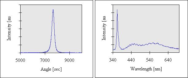
Figure 2. Typical DC X-ray diffraction curve and PL spectrum of GaN layer.
The FWHM of the DC X-ray curve is typically between 100 and 300 arcsec, but the narrowest curve measured up to now had a FWHM of 67 arcsec (thickness 0.75 μm). The room temperature PL-curve shows a band edge emission around 365 nm (FWHM = 65 meV) and a low intensity deep level emission in the yellow band. Occasionally a low intensity peak appears in the blue band, but the origin of this emission is not completely clear. The fringes which are visible in the blue to yellow band indicate an optically smooth surface. We found that by increasing the growth temperature of the epilayer the deep level emission becomes negligible. For layers grown at 950 °C the ratio band edge emission to deep level emission was very low, so that the emission spectrum was dominated by the deep level emission. By increasing the growth temperature to 1050 °C the yellow emission decreased significantly . When the growth was conducted with mixed hydrogen/nitrogen carrier gas at 1070 °C the yellow emission band disappeared (see Figure 3). The growth temperature of the nucleation layer also had a strong influence on the band edge to deep level emission ratio. The highest ratio was measured on layers with a nucleation layer growth temperature of 475 °C [5]. Most of the 1 μm thick undoped GaN films showed an n-type background carrier concentration of approximately 51017 /cm3 and a Hall mobility of 150 cm2/Vs. For 2.5 μm thick films the mobility increased to 245 cm2/Vs. The growth speed was typically 0.75 to 1 μm/hour. To overcome the problem of low growth speed, growing at low pressure (70 Torr) and with H2/N2 mixed carrier gasses was tried. This resulted in higher growth speeds (2 to 3 μm/hour), but the surface of the layers was covered with hexagonal pyramids. Under these growth conditions it was more difficult to achieve a mirror like surface. This can be explained by the fact that the growth rate increases relatively more in the Reference Akasaki and Amano[1] direction then the lateral [01

Figure 3. PL spectrum for GaN layers deposited a different temperatures.
3.2 N-type doped GaN
Doping GaN with SiH4 is very efficient, since Si seems to incorporate very well in GaN. Consequently high doping levels can be achieved with low SiH4 flows. Figure 4a shows the variation of doping level with varying dopant flow. It is clear that the required flow to achieve a certain doping level is very critical. This non-linear curve is very similar to a previous report of J.D. Guo Reference Guo, Lin, Feng, Pan, Chi and Lee[6], although he used much higher flow rates ( 0 to 10 sccm of 100 ppm SiH4). In our case very high flow rates (4.5 nmol/min) led to a deterioration of the GaN layer; the surface of the sample became very rough and many pits appeared. This overdoping effect is not uncommon Reference Guo, Lin, Feng, Pan, Chi and Lee[6] Reference Nakamura, Mukai and Senoh[7]. At flows in the range of 1 to 2.8 nmol/min the morphology was smooth. The quality of the doped GaN layers, as judged by DC X-ray measurements, was very good (FWHM = 150 to 300 arcsec) . The carrier concentration was determined using Hall measurements. The mobility of the layers was quite low compared to other reports, but it changed accordingly for different doping levels Reference Gaskill, Wickenden, Doverspike, Tadayon and Rowland[8] Reference Keller, Keller, Kapolnek, Jiang, Wu, Masui, Wu, Heying, Speck, Mishra and Denbaars[9]. Similarly the mobility decreased for higher carrier concentrations. Figure 4b illustrates the dependence of Hall mobility on the carrier concentration. The PL intensity increased with increasing doping level, but the peak also broadened (FWHM = 120 meV). In Figure 5 two PL-curves are compared: the low intensity peak is measured on undoped GaN, the high intensity peak is measured on a n-type doped GaN layer with a carrier concentration of 2.2 1019 /cm3.

Figure 4a. Doping level versus SiH4 flow.
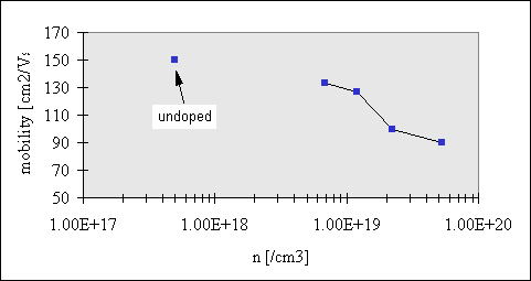
Figure 4b. Hall mobility versus carrier concentration.

Figure 5. PL-curve of undoped and highly n-type doped GaN layer.
4. Conclusion
GaN and n-type doped GaN films were grown on (0001) sapphire in a vertical rotating disk MOCVD reactor. Because of the variety of growth parameters which can be altered, the growth process is still very critical. The growth process was optimised for deposition of GaN layers. As judged by X-ray diffraction, photoluminescence characterisation and electrical characterisation these films exhibit promising quality. Controlled n-type doping with SiH4 has been achieved up to a level of 2.8 1019/cm3, without deterioration of the surface.
Acknowledgments
Wim Van der Stricht thanks the IWT for financial support and Ann Janssens for carrying out X-ray and PL measurements in the framework of her graduate thesis.


