


1. Introduction
The interest for III-V nitride semiconductors is continuously increasing. The fact that GaN has a wide direct band gap of 3.5 eV at room temperature Reference Monemar[1] makes it useful in lasers Reference Nakamura, Senoh, Nagahama, Iwasa, Yamada, Matsushita, Kiyoku, Sugimoto, Kozaki, Umemoto, Sano and Chocho[2] and light emitting diodes (LED) Reference Nakamura, Senoh, Iwasa and Nagahama[3] with green or blue emission. Due to the short wavelength, blue lasers could write at least four times more information on optical storage devices such as compact discs, than the currently used red lasers. Another application for blue lasers is in dentistry for curing composite filling material Reference Mills[4].
For the device fabrication the knowledge about e.g. sample polarity, surface termination, and surface stoichiometry of the GaN sample in use is crucial for success. But, so far the information about the actual sample polarity, surface termination, and surface stoichiometry under investigation has not always been stated in present published work. This makes conclusions about the similarities and differences between the two polarities harder to achieve. For the assignment of sample polarity several articles Reference Rouviere, Weyher, Seelmann-Eggebert and Porowski[5] Reference Seelmann-Eggebert, Weyher, Obloh, Zimmermann, Rar and Porowski[6] Reference Sumiya and Fuke[7] have been published on this issue, presenting simple methods to employ. Still, these have not always been used. For the determination of the termination and surface stoichiometry, x-ray photoelectron spectroscopy (XPS) can be employed. But, this technique is not always available at the laboratory or beamline, especially not during ultraviolet photoelectron spectroscopy (UPS) measurements. Reliable data is needed about different binding energies (EB) of the GaN components to facilitate the determination of surface termination and stoichiometry for use as further reference. Several published works Reference Hedman and Martensson[8] Reference Beach, Piquette and McGill[9] Reference Lai, Yeh, Hwang, Hwang, Chen and Wei-Hsiu[10] Reference Li, Sumiya, Fuke, Yang, Que, Suzuki and Fukuda[11] Reference Bermudez and Long[12] Reference King, Barnak, Bremser, Tracy, Ronning and Davis[13] have been presenting data from GaN including binding energies and possible binding configurations, which can be used as guide lines. An in-depth analysis, using high-resolution XPS (HRXPS), of the binding energies, line shape parameters, and possible binding configurations has not been previously reported.
In this work we address several of the questions raised. This paper is based on our earlier work Reference Widstrand, Magnusson, Johansson, Moons, Gurnett, Yeom, Miki and Oshima[14], which presents the preparation method to achieve surface stoichiometry for a Ga-polar GaN(0001)-1×1 sample. In this paper we focus on the in-depth analysis of the Ga 3d and N 1s core levels of such a sample using HRXPS. The knowledge about these EB and line shape parameters for a stoichiometric Ga-polar GaN(0001)-1×1 sample is at the moment limited. We also report on the Ga 3d EB and line shape parameters from a Ga overlayer deposited on the stoichiometric surface. Spectral signatures from remaining amounts of O 1s and C 1s are included for reference.
2. Experimental details
The sample studied was a wurtzite structure GaN film, n-doped (Si) with a carrier concentration of n=4.65×1017 cm-3 and a Hall electron mobility of µH=376.5 cm2V-1 s-1. The doped GaN layer had a thickness of 0.72 µm, on top of an undoped GaN layer of 1.0 µm and a 20 nm buffer layer, grown on a sapphire (Al2O3) substrate by metal organic chemical vapour deposition (MOCVD). The sample surface normal was in the (0001) Ga-polar direction, as determined by an etching method Reference Rouviere, Weyher, Seelmann-Eggebert and Porowski[5] Reference Widstrand, Magnusson, Larsson, Johansson, Gustafsson, Moons, Miki, Oshima and Yeom[15]. The sample was cleaned ultrasonically in acetone, ethanol, and methanol, and dried in a nitrogen gas flow. The sample was then mounted directly upon a tantalum (Ta) foil, with Ta clips on the surface to avoid surface charging, and introduced into the ultra high vacuum (UHV) system. For the heating of the sample, resistive heating of the Ta foil was used and the temperature was measured with an infrared pyrometer.
The XPS experiment was performed at MAX-Lab synchrotron radiation laboratory in Lund, Sweden. The measurements were performed on the 38 period undulator beamline I311 Reference Nyholm, Andersen, Johansson, Jensen and Lindau[16], with the photon energy range 50-1500 eV. The beamline is equipped with a hemispherical electron energy analyser (SCIENTA SES200) and a modified SX-700 monochromator with a 1220 lines/mm grating, a spherical focusing mirror and a movable exit slit. The total energy resolution of the analyser and the monochromator was set to 40-100 meV in this experiment. The base pressure in the analyser chamber was 7×10-11 mbar. The Fermi level position was determined from a clean platinum (Pt) foil in good electrical contact with the sample. The angle between the incidence of the light and the analyser lens is 55° and all of the presented spectra were recorded in normal emission. All presented spectra are normalised to the photon current and the number of sweeps. The synchrotron radiation is linearly polarised with the polarisation in the plane of the photoelectron detection.
Before the spectra were acquired, the sample was first prepared as described in detail by Widstrand et al. Reference Widstrand, Magnusson, Johansson, Moons, Gurnett, Yeom, Miki and Oshima[14] and can be summarised as follows; step (a): outgassing, step (b): series of NH3 flux annealing, step (c): Ga deposition at room temperature followed by vacuum annealing, and step (d): Ga deposition during heating of the sample followed by NH3 flux anneal. This preparation yields a surface stoichiometry close to 1, with low amounts of contaminants, such as oxygen and carbon, left on the surface. The low electron energy diffraction (LEED) pattern associated with this stoichiometric surface showed a clear and sharp 1×1 reconstruction.
The deposition of Ga on the stoichiometric surface was done by resistive heating of a tantalum (Ta) boat containing Ga. A piezoelectric crystal thickness monitor measured the final thickness to be equivalent to about 1.5 monolayer (ML) (1 ML is equivalent to about 9.8×10¹⁴ Ga atoms/cm2). The Ga deposition was performed with the sample held at room temperature (RT). After the deposition a 1×1 LEED pattern (not shown) of low intensity was found with rather large spots.
For the identification of the different components in the spectra the line shapes of the different components were calculated by a non-linear least-squares fitting program and fitted to the experimental spectra after subtraction of the background. The line shape of the structures in a spectrum can be interpreted by so called Lorentzian and Gaussian broadening. The former is related to the finite lifetime of the core hole and the Gaussian broadening is mainly due to the instrumental resolution, structure defects and contribution from phonons. For metallic components it may also be necessary to add an asymmetry factor α Reference Doniach and Sunjic[17] to the Lorentzian shape, which expresses itself as a higher intensity at the higher EB side of the peak. This phenomenon is caused by the fact that the creation of a core hole can be accompanied by excitation of an electron hole pair near the Fermi level Reference Wertheim and Dicenzo[18].
3. Results and Discussion
3.1 Core levels
The following section present the experimental spectra together with the fitting results from the line shapes of the Ga 3d and N 1s core levels from the stoichiometric surface. The Ga 3d spectrum after Ga deposition on the stoichiometric surface is also presented. The photon energies used in this work for all core levels give an escape depth of the photoelectrons of 3-5 Ångström (Å), i.e. surface sensitive measurements. We compare the resulting parameters of the line shapes listed in Table 1-4, with those reported for other GaN experiments. When no data were accessible from GaN samples we refer for comparison to results from experiments on other III-V semiconductors e.g. gallium arsenide (GaAs), gallium phosphide (GaP), and gallium antimonide (GaSb).
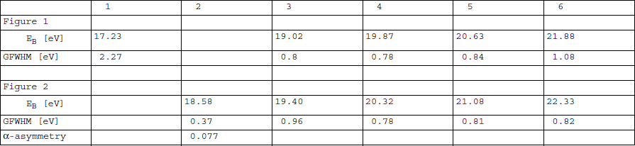
Table 1. The resulting parameters for the line shape analysis of Ga 3d in Figure 1 and Figure 2. The branching ratio was found to be 0.64, and the EB relative EF is given for the d5/2 component for the structures labelled 2-6. The S-O splitting was 0.46 eV and the LFWHM was 0.13 eV for all structures.
3.1.1 Ga 3d
We have studied the Ga 3d core level spectrum under two different surface conditions. The first was on a cleaned stoichiometric surface and the second was after Ga deposition on the stoichiometric surface, see Figure 1 and Figure 2, respectively. The experimental spectra are shown together with the corresponding line shape analysis of the bulk and chemically shifted structures and the residual.

Figure 1. Photoelectron spectrum of Ga 3d from the stoichiometric GaN(0001)-1×1 sample. The experimental data is represented by circles, the solid lines show the components of the line shape, the resulting fit, the subtracted linear background, and the residual, see Table 1 for parameter details.

Figure 2. Photoelectron spectrum of Ga 3d from the GaN(0001)-1×1-Ga surface. The experimental data is represented by circles, the solid lines show the components of the line shape, the resulting fit, the subtracted linear background, and the residual, see Table 1 for parameter details.
For the fitting of the spectra in Figure 1 and Figure 2, we have used a theoretical calculated branching ratio (BR) of 0.67 (2:3) as a starting parameter value. For the determination of the spin-orbit (S-O) split and the Lorentzian width at full width at half maximum (LFWHM), a line shape analysis was first made of the well-resolved Ga 3d component, structure 2, found at the low EB side in Figure 2. The values of the S-O split, which was found to be 0.458 eV and the LFWHM, which was found to be 0.13 eV, were then held fixed during the analysis for structures 2-6. The EB of the peaks and the Gaussian widths at full width at half maximum (GFWHM) were set as free parameters in the fitting analysis. The found parameter values for the calculated line shapes shown in Figure 1 and Figure 2 are summarised in Table 1.
Table 1. The resulting parameters for the line shape analysis of Ga 3d in Figure 1 and Figure 2. The branching ratio was found to be 0.64, and the EB relative EF is given for the d5/2 component for the structures labelled 2-6. The S-O splitting was 0.46 eV and the LFWHM was 0.13 eV for all structures.
The value of 0.46 eV for the S-O split found for the Ga 3d components is the same value as reported by Kowalski et al. Reference Kowalski, Plucinski, Kopalko, Iwanowski, Orlowski, Johnson, Grzegory and Porowski[19] for a bulk GaN(000-1)−1×1 samples and by Beach et al. Reference Beach, Piquette and McGill[9] for a GaN(000-1)-3 × 3 MBE grown sample. This result is also consistent with the result of 0.45 eV for GaAs, GaP, and GaSb samples reported by Stietz et al. Reference Stietz, Sloboshanin, Engelhard, Allinger and Goldmann[20], Duó et al. Reference Duo, Sancrotti, Cosso, D‘Addato, Ruocco, Nannarone, Norman and Weightman[21], and Franklin et al. Reference Franklin, Rich, Samsavar, Hirschorn, Leibsle, Miller and Chiang[22]. The ratio between the relative areas was found to be 0.64, which matches also with the theoretical branching ratio of 0.67, and is similar to previous results Reference Beach, Piquette and McGill[9] Reference Kowalski, Plucinski, Kopalko, Iwanowski, Orlowski, Johnson, Grzegory and Porowski[19]. For other III-V semiconductors the ratio range is 0.56-0.66 according to ref. Reference Stietz, Sloboshanin, Engelhard, Allinger and Goldmann[20] Reference Duo, Sancrotti, Cosso, D‘Addato, Ruocco, Nannarone, Norman and Weightman[21] Reference Franklin, Rich, Samsavar, Hirschorn, Leibsle, Miller and Chiang[22]. The LFWHM value 0.13 eV can be compared with the published values 0.155 eV Reference Stietz, Sloboshanin, Engelhard, Allinger and Goldmann[20] and 0.17 Reference Duo, Sancrotti, Cosso, D‘Addato, Ruocco, Nannarone, Norman and Weightman[21] eV for Ga 3d features associated with GaAs and GaP, respectively. We have not found any reference reporting on the LFWHM of the Ga 3d feature from a GaN sample.
Structure 4 has an EB of 19.87 eV rel. EF for the d5/2 component for the stoichiometric sample and is the mayor component of the spectrum and we interpret it as originating from bulk GaN. Published values for the EB of the bulk Ga 3d core level of a GaN sample are 20.6 eV by Tracy et al. Reference Tracy, Mecouch, Davis and Nemanich[23], 19.74 eV by Hedman et al. Reference Hedman and Martensson[8], 20.5 eV by Lai et al. Reference Lai, Yeh, Hwang, Hwang, Chen and Wei-Hsiu[10], and 19.9 and 20.23 eV by Kowalski et al. Reference Kowalski, Plucinski, Kopalko, Iwanowski, Orlowski, Johnson, Grzegory and Porowski[19] Reference Kowalski, Iwanowski, Sadowski, Kowalik, Kanski, Grzegory and Porowski[24], relative EF. These discrepancies between the published data can be explained by the fact that the Fermi level position in the band gap is easily moved by changes in band bending. This phenomenon can be triggered by modifications in the electronic structure on the surface e.g. a non-stoichiometric surface or chemisorption. In addition, except for the measurement made by Lai et al. Reference Lai, Yeh, Hwang, Hwang, Chen and Wei-Hsiu[10], previous measurements have not been carried out at a HRXPS beamline. A better way to determine the EB of the bulk Ga 3d core level is to measure its distance to the valence band maximum (VBM), because this value is a constant for the stoichiometric GaN(0001)-1×1 sample. To determine the exact VBM position it is necessary e.g. to do an angle-resolved ultraviolet photoemission (ARUPS) study and by means of that carefully decide the VBM.
Structure 4 shows a shift by 0.45 eV to higher EB 20.32 eV after the Ga deposition. A similar shift is present for all structures in Figure 2. We interpret this EB shift as due to enhanced band bending downwards, because N1s and the Ga 3p features (spectra not shown) also show similar shifts in EB after Ga deposition. Our interpretation that the EB is shifted towards higher values due to band bending upon increasing the presence of Ga on the surface is supported by observations made by Lai et al. Reference Lai, Yeh, Hwang, Hwang, Chen and Wei-Hsiu[10].
The structure labelled 3 in Table 1 is visible in both Figure 1 and 2 but with different integrated area relative the bulk structure. The relative integrated area of structure 3 to the bulk structure 4 is 4.5 times higher in Figure 2 after the Ga deposition than in Figure 1. This may imply that structure 3 is related to surface Ga bond to an extra Ga atom instead of a N atom in different (binding) configurations, which may imply a larger bond length yielding a relaxation outwards. The EB differences between structure 3 and the bulk, structure 4, are 0.85 eV and 0.92 eV, for Figure 1 and Figure 2, respectively. The EB differences from the bulk structure 4 and structure 3 are supported by the results of Lai et al. Reference Lai, Yeh, Hwang, Hwang, Chen and Wei-Hsiu[10].
The surface structure labelled 5 has an integrated area relative the bulk of 1.2 times larger for the stoichiometric surface in Figure 1 than in Figure 2. This may imply that structure 5 is related to Ga atoms at the surface in a configuration that is altered by the Ga deposition. Structure 5 is interpreted as Ga with an empty dangling bond at the surface, which yields a relaxation inwards of the atom and a tighter binding configuration. This structure is associated with the clean and ordered surface of a Ga-polar GaN(0001) samples surface. The interpretation that the surface shifted component for the cation Ga atom is towards higher EB for compounds as GaN is supported by Mönch Reference Mönch[25].
Structure 6 has an integrated area relative the bulk structure 4 that is 1.6 times larger in Figure 1 compared to Figure 2, so this component is apparently affected by the Ga deposition. The EB of structure 6 is 21.88 eV for the stoichiometric surface. Kowalski et al. Reference Kowalski, Plucinski, Kopalko, Iwanowski, Orlowski, Johnson, Grzegory and Porowski[19] and Bermudez et al. Reference Bermudez and Long[12] have found evidence for Ga-O bonding features on GaN samples in this EB region, which strengthens our interpretation of structure 6 as due to oxidation of the surface. We have estimated the amount of structure 6 in Figure 1 compared to the bulk feature, structure 4, by using the formula from Reference Beach, Piquette and McGill[9]

where χ is the fraction of surface coverage in ML, β is the ratio of measured surface to bulk integrated peak intensities (0.03 in our case), m is the number of atomic double layers in the crystal, λ is the mean free path expressed in the distance between Ga planes (2 in our case), and α is the collection angle measured from the surface normal (0 in our case). We found a surface coverage of 0.08 ML, which matches the amount of about 0.10 ML O found to be left on the stoichiometric surface Reference Widstrand, Magnusson, Johansson, Moons, Gurnett, Yeom, Miki and Oshima[14]. Possible configurations are digallium oxide (Ga2O) and digallium trioxide (Ga2O3) Reference King, Barnak, Bremser, Tracy, Ronning and Davis[13] Reference Kowalski, Plucinski, Kopalko, Iwanowski, Orlowski, Johnson, Grzegory and Porowski[19].
The component (labelled structure) 2 at EB 18.58 eV is only present for the Ga-covered surface in Figure 2. We interpret this as emission from a Ga overlayer, because it appears after the additional deposition of Ga. The absence of structure 2 in Figure 1 is because the Ga to N ratio is about 1 for that surface Reference Widstrand, Magnusson, Johansson, Moons, Gurnett, Yeom, Miki and Oshima[14], so there is no Ga overlayer left on the surface after the surface preparations. Antonides et al. Reference Antonides, Janse and Sawatzky[26] and Fuggle et al. Reference Fuggle and Martensson[27] have studied the Ga core levels of a pure metallic Ga sample. For a metallic sample the Fermi level and the VBM are at the same position. This makes the determination of the correct value of the EB for the metallic core levels easier but unfortunately they could not resolve the Ga 3d metallic feature in the two S-O components. Antonides et al. Reference Antonides, Janse and Sawatzky[26] report an EB of 18.4 eV and Fuggle et al. Reference Fuggle and Martensson[27] report 18.7 eV rel. EF, in fair agreement with our observation in Figure 2, even though their results are from a pure Ga sample and ours are for a Ga-covered GaN sample. Kowalski et al. Reference Kowalski, Plucinski, Kopalko, Iwanowski, Orlowski, Johnson, Grzegory and Porowski[19] have annealed a cleaned bulk N-polar GaN sample until an additional Ga 3d component appeared in the spectrum at 18.2-18.5 eV. Lai et al. Reference Lai, Yeh, Hwang, Hwang, Chen and Wei-Hsiu[10] have found an EB of 18.9 eV for a similar structure on a sputtered GaN sample. The EB difference for the overlayer associated Ga, structure 2, relative the surface structure 3 and to the bulk structure 4, is 0.82 eV and 1.74 eV, respectively, in Figure 2. The interpretation of structure 2 as associated with a Ga overlayer and the EB differences between structures 2, 3, and 4 are supported by the results of Lai et al. Reference Lai, Yeh, Hwang, Hwang, Chen and Wei-Hsiu[10].
The α-asymmetry parameter Reference Doniach and Sunjic[17] value was found to be 0.077 by the fitting routine for structure 2. The result closely match 0.09 obtained by Stietz et al. Reference Stietz, Sloboshanin, Engelhard, Allinger and Goldmann[20] for a metallic Ga 3d structure from a GaAs sample. We have estimated the Ga surface coverage for structure 2 in Figure 2 by using formula (1). Here, the ratio between the integrated peak intensities of surface structure 2 to the bulk structure 4 was calculated to 0.56, yielding a Ga overlayer coverage of 0.9 ML.
The GFWHM for structure 2 was found to be 0.37 eV. This value is much smaller than for the other Ga 3d structures, which may indicate that the deposited Ga has formed an ordered metallic overlayer with a reduced phonon contribution. The LEED pattern was of lower quality after the metallic deposition on the stoichiometric surface. This together with the low GFWHM may imply that the deposited Ga formed ordered incommensurate islands 2 dimensions (D) or 3D on the surface instead of being evenly distributed.
For the stoichiometric surface in Figure 1 there is a weak and broad (GFWHM=2.27 eV) feature at EB 17.23 eV labelled structure 1. This structure is fitted by a singlet and is not visible in Figure 2, because of the partial overlap with structure 2. The assignment has already been done by Ding et al. Reference Ding, Neuhold, Weaver, Haberle, Horn, Brandt, Yang and Ploog[28] as due to emission from N 2s-character states from Ga 3d-N 2s hybridisation.
3.1.2 N 1S
The N 1s spectrum together with the line shape analysis is presented in Figure 3 and the resulting line shape parameters for the N 1s structure are summarised in Table 2.

Figure 3. Photoelectron spectrum of N 1s from the stoichiometric GaN(0001)-1×1 surface. The experimental data is represented by circles, the solid lines show the components of the line shape, the resulting fit, the subtracted integrated background, and the residual, see Table 2 for parameter details.
Table 2. The resulting parameters for the N 1s core level line shape analysis for Figure 3. The LFWHM was found to be 0.24 eV for all structures.

Structures 3-6 all have a higher EB than the bulk structure 2, and structure 1 has a lower EB . For the interpretation of the structures spectra were recorded after sample treatment step (c): Ga deposition at room temperature followed by vacuum annealing, taken at an emission angle of 0 ° and at a grazing emission angle of 60 °, see Figure 4. After this step there is still an excess of Ga on the surface and minor effect of NH 3, for further details see ref. Reference Widstrand, Magnusson, Johansson, Moons, Gurnett, Yeom, Miki and Oshima[14]. The integrated areas of structure 1 and 3 relative the area of structure 2, shows an increase with a factor of about 2 in the spectrum taken at 60° emission angle compared to spectrum taken at an emission angle 0°. The weaker structures 1 and 3-6, are thus surface related and the main peak, structure 2, corresponds to the bulk contribution from GaN. The energy shifts of structure 1 and 3-6 relative the bulk structure 2 are -0.54, 0.47, 1.05, 1.76, and 2.94 eV, respectively. Structure 1 and 3 are interpreted as surface shifted components of the stoichiometric, clean Ga-polar GaN(0001)-1×1 surface. The assignment of structure 1 is supported by Mönch Reference Mönch[25], because the surface core level shift for the anion N atom on the ordered surface is towards lower binding energy compared to the bulk. However, the increased EB of structure 3 is not predicted by the theory of Mönch. A possible interpretation of this structure is that it is due to emission from N adatoms bonded to the topmost Ga atoms, similar to a continued bulk configuration. To still achieve stoichiometry, additional Ga atoms on the surface should be necessary, and these are proposed to be bonded to the topmost Ga atoms. These excess Ga atoms, which were seen as structure 3 in the Ga 3d line, cause a surface shift for the neighboring N atoms to lower binding energy possibly overlapping with emission from the ordered surface structure 1. The relative increased intensity of structure 1 in Figure 4, as compared to structure 3, also support this interpretation since there is a further excess of surface Ga after this step of the surface treatment.

Figure 4. Photoelectron spectrum of N 1s recorded after treatment step (c): Ga deposition at room temperature followed by vacuum annealing, taken at an emission angles of 0° and at a grazing emission angle of 60°. The experimental data is represented by circles, the solid lines show the components of the line shape, the resulting fit, the subtracted integrated background, and the residual.
The binding energy of the bulk component of 398.24 eV rel. EF closely matches the value obtained by Tracy et al. Reference Tracy, Mecouch, Davis and Nemanich[23], who reports an EB of 398.0 ±0.1 eV for a stoichiometric MOCVD grown GaN(0001)-1×1 surface prepared by NH3 annealing. It differs from the results of 397.4 and 397.5 eV for Ar and N sputtered surfaces, respectively, reported by Lai et al. Reference Lai, Yeh, Hwang, Hwang, Chen and Wei-Hsiu[10]. This variation in previously reported EB might be assigned to different amount of band bending as discussed earlier. Li et al. Reference Li, Sumiya, Fuke, Yang, Que, Suzuki and Fukuda[11] also reports on a similar N 1s line shape from as-grown and potassium hydroxide (KOH) etched surfaces of GaN samples with both Ga- and N-polarity. Li et al. concludes that the weaker structures at the high EB side are due to N-H2 and N-H3 formations. This may be a possible explanations of the origin of structure 4-6, because H is provided to the surface during the NH3 flux anneal.
Structure 5 and 6 in Figure 4 is not visible in Figure 5, which implies sensitivity for Ga adsorption.

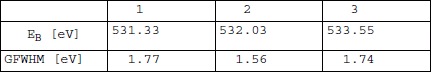
Figure 5. Photoelectron spectrum of O 1s from the stoichiometric GaN(0001)-1×1 surface. The experimental data is represented by circles, the solid lines show the components of the line shape, the resulting fit, the exponential background, and the residual, see Table 3 for parameter details.
Table 3. The resulting parameters for the O 1s core level line shape analysis for Figure 5. The LFWHM was found to be 0.26 eV for all structures.
We could not identify any N-O bonding peak, which should appear at binding energies at least 5 eV higher than the bulk peak, according to results on AlN Reference Gredelj, Gerson, Kumar and Cavallaro[29] surfaces. This may indicate that the O atoms do not form bonds to N atoms on the surface. This finding is also supported by Elsner et al. Reference Elsner, Gutierrez, Hourahine, Jones, Haugk and Frauenheim[30] who have used a self-consistent-charge density-functional tight-binding (SCC-DFTB) method to calculate structures where some of the Ga atoms in the adlayer were replaced by O atoms so that N-O bonds could be formed. According to these calculations such structures would have very high formation energy, suggesting that in any stable configuration only Ga-O bonds can exist. To confirm the interpretation a HRXPS study is needed, where a cleaned stoichiometric GaN sample is, e.g., exposed to O atoms.
However, the presence of oxynitrides have been reported by Fukui et al. Reference Fukui, Ichikawa, Yamamoto and Kamada[31] and Lee et al. Reference Lee, Kim, Shin and Kim[32] on indium nitride (InN) surfaces. Kim et al. Reference Kim and Yeom[33] have reported on a NH3 study on a silicon (Si) surface. They have found both Si-NH2, Si=NH, and Si3≡N species in the N 1s spectra, which further strengthen the assumption of the existence of N-NHx (x<3) bonds.
3.2 Residual contaminants
3.2.1 O 1s
The O 1s experimental data and calculated line shapes for the stoichiometric surface are presented in Figure 5, see Table 3 for details of the parameters.
The line shape analysis of the experimental spectra of the O 1s feature reveals three different components, labeled structure 1-3 in Table 3. The possible configurations causing the appearance of these three structures are O atoms bonding to Ga atoms e.g. Ga2O, Ga2O3 Reference King, Barnak, Bremser, Tracy, Ronning and Davis[13], see the interpretation for structure 6 in Figure 1 and 2, see Table 1. Other possible interpretations are chemisorbed oxygen and O-H bonding Reference Li, Sumiya, Fuke, Yang, Que, Suzuki and Fukuda[11] Reference King, Barnak, Bremser, Tracy, Ronning and Davis[13].
3.2.2 C 1s
The C 1s core level spectrum is complex and the calculated line shapes for the stoichiometric surface show 5 different components, which are shown in Figure 6. We have summarised the resulting parameters in Table 4.

Figure 6. Photoelectron spectrum of C 1s from the stoichiometric GaN(0001)-1×1 surface. The experimental data is represented by solid circles, the spectra after subtraction of an integrated background is shown by open circles, the solid lines show the components of the line shape, the resulting fit, and the residual, see Table 4 for parameter details.
Table 4. The resulting parameters of C 1s core level line shape analysis for Figure 6. The LFWHM was found to be 0.17 eV for all structures.

The C 1s experimental structure of the stoichiometric surface, see Figure 6, contains two clearly revealed components labeled structure 1 and 2, in Table 4. In addition, the tail on the high EB side contains three broad structures revealed by the line shape analysis. A similar complex line shape of the C 1s feature has been published by Gredelj et al. Reference Gredelj, Gerson, Kumar and Cavallaro[29] for AlN, where the structures were identified as C-H, C-O, C=O, and O=C-O bonding with increasing EB.
In this study we can not confirm or deny these interpretations of both the O 1s and C 1s structures, because a HRXPS study should be done, where a cleaned stoichiometric GaN sample is, e.g., exposed to O atoms and C atoms.
4. Conclusions
4.1 Core levels
We present an in-depth analysis of electron binding energies and line shapes of the bulk and surface components of the Ga 3d and N 1s core levels. The Ga 3d feature for the stoichiometric surface is resolved into a bulk and three different surface structures compared to the bulk structure. The surface shifted structures have lower and higher binding energies by -0.76, 0.85, and 2.01 eV, respectively. The bond which is shifted to higher EB by 0.85 eV is interpreted as surface Ga with one of the N bonds replaced by an empty dangling bond with the stoichiometric clean and ordered Ga-polar GaN(0001)-1×1 surface. The surface structure with lower EB originates from surface excess Ga, where one of the N bonds is replaced by a bond to a Ga atom. The structure with highest EB is identified as oxidised gallium.
For our sample this would indicate a close to stoichiometric surface according to the relative high amount of dangling bonds, but with a slightly excess of Ga present on the surface. The existence of oxidised Ga also reveals that the surface still has a small amount of contaminations left on the surface.
After Ga deposition on the stoichiometric surface we found a Ga 3d structure originating from a Ga overlayer with an EB of 18.58 eV rel. E F for the 3d5/2 component. The surface shift for the Ga 3d5/2 component from the Ga overlayer is -1.74 eV relative the bulk GaN. The Ga deposition also led to an EB shift towards higher values rel. E F, indicating an upward movement of the Fermi level in the band gap at the surface.
For the N 1s feature five surface shifted components were found with shifts with respect to the bulk structure 2 of -0.54, 0.47, 1.05, 1.76, and 2.94 eV, respectively. The two structures at -0.54 eV and 0.47 eV are interpreted as originating from the stoichiometric, clean Gapolar GaN(0001) surface with both N and Ga adatoms. The other structures may originate from N-Hx formations formed during the NH3 flux anneal. There is a strong need for calculations of surface core level shifts in this system.
The variation of previously reported EB of the core levels of Ga 3d and N 1s may be assigned to different amount of band bending, especially when comparisons are made between different surface methods.
4.2 Residual contaminants
The spectra of O and C are both very complex and further specific HRXPS studies must be performed to facilitate the identification of the different contributions.
Acknowledgments
We would like to thank the staff of MAX-Lab synchrotron radiation laboratory for their support. This work was supported by the Swedish Research Council. We also thank H.W. Yeom and H. Miki for growing and providing the samples.


