


Introduction
A state-of-the-art CMOS chip comprises not only billions of transistors, but also 10 or more levels of nanometer-to-micrometer-wide metal lines buried in interlevel oxides to interconnect the transistors [Reference Turkane and Kureshi1]. For quality control and failure analysis, it is a challenge to inspect these interconnect lines that crisscross through the oxides. For this purpose, although X-ray or electron microscopy can be used, they can damage the oxides. Traditional scanning probes such as atomic force microscope (AFM) and scanning tunneling microscope (STM) can provide nanometer resolution non-destructively. However, they are sensitive only to surface properties. In comparison, scanning microwave microscope (SMM), an emerging derivative of AFM or STM, can penetrate up to a micrometer in oxides and other dielectrics [Reference Smoliner, Huber, Hochleitner, Moertelmaier and Kienberger2]. Additionally, being sensitive to electrical properties, SMM shows sharp contrast between metal and dielectric. SMM achieves nanometer resolution through near-field interaction between the nanometer probe and the sample, despite the relatively large microwave wavelength. SMM is non-destructive because the energy of the microwave photons is on the order of 10 µeV.
Recently, SMM was successfully used to image 1.2 µm-wide Al-Si-Cu lines buried under plasma-deposited tetraethylorthosilicate either 800 or 2300 nm thick with 900 ± 70 and 1200 ± 260 nm spatial resolution, respectively [Reference You, Ahn, Obeng and Kopanski3]. Most recently, SMM was used to image 80 µm-wide TiN-Ti-Al lines buried under atomic-layer deposited (ALD) aluminum oxide 20 nm thick with 600 nm sharpness [Reference Jin, Xiong, Marstell, Strandwitz, Hwang, Farina, Göritz, Wietstruck and Kaynak4]. The experiment was repeated in water to simulate high-k dielectric and found the sharpness degraded by approximately 60%. This paper reports SMM of TiN-Ti-Al lines buried under 20 nm-thick ALD aluminum oxide with 190 ± 70 nm resolution both in and out of water. The reason for such significant improvement is detailed below.
Experimental setup
TiN-Ti-caped Al interconnect lines approximately 0.5 µm thick were fabricated by a state-of-the-art 130 nm SiGe BiCMOS process on a 200 mm-diameter high-resistivity (10 kΩ·cm) Si wafer [Reference Mai and Kaynak5]. Lines with designed widths of 160 and 360 nm (actual widths 190 and 390 nm due to process bias as determined by SMM) were embedded in 1.3 µm thick SiO2, then chemo-mechanically polished to a flatness of approximately 70 nm as indicated by the AFM profile in Fig. 1. Thereafter the wafer was diced into 25 mm × 15 mm chips. To simulate buried interconnect lines, some of the chips were coated with 20 nm of ALD Al2O3 at 300 °C. The conforming ALD did not alter the surface topography significantly (Fig. 1(b)), which minimizes the so-called “topography cross-talk” difference in SMM [Reference Smoliner, Huber, Hochleitner, Moertelmaier and Kienberger2] between samples with and without oxide coating. Otherwise, the SMM contrast between the two sets of samples would have been complicated by the difference in topography through its influence on the parasitic capacitance with the probe. Defining the image sharpness by the transition width from 25 to 75% height [Reference You, Ahn, Obeng and Kopanski3], Fig. 1(b) shows also that the AFM sharpness is approximately 80 nm, which is actually inferior to that of SMM, because the AFM scan parameters were not fully optimized giving the emphasis on SMM in this study.
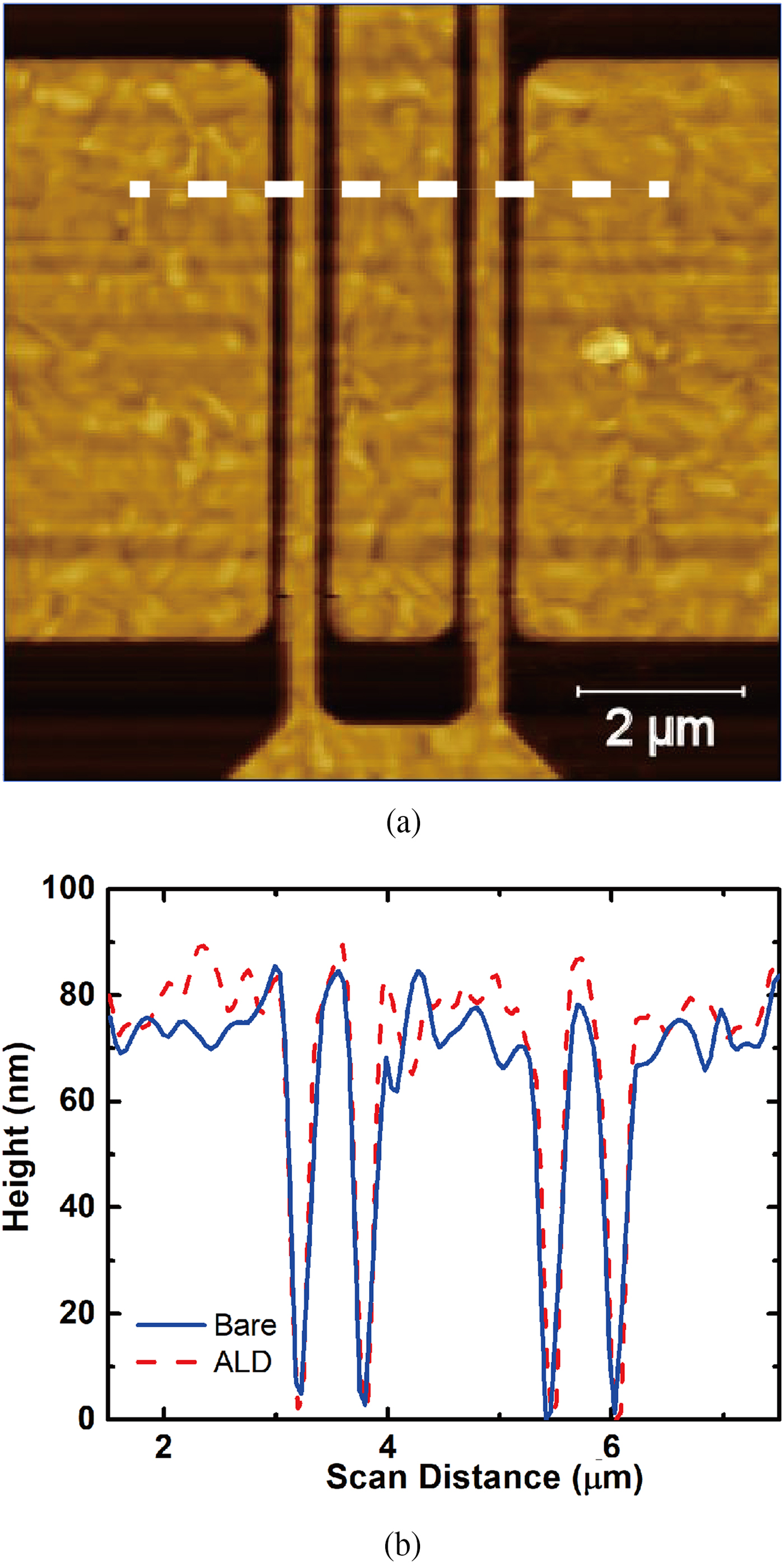
Fig. 1. AFM (a) image and (b) linear scan of 190 nm-wide bare (—) aluminum lines. The image of buried lines is visually indistinguishable from that of bare lines and, hence, not shown. The profile of the buried lines is also very similar to that of bare lines as indicated by dashed line (- - -) in (b). Dashed line in (a) indicates where linear scans were taken.
The two sets of chips, with and without oxide coating, provided a good contrast between bare and buried metal lines. The aluminum lines on the uncoated chips were prevented from oxidation by TiN. The TiN and Ti layers, being nanometer thin, did not significantly change the electrical properties of the metal lines from that of pure Al. For tests in water, the chips were placed on the bottom of a petri dish that is filled with approximately 5 mm of deionized water, sufficient to immerse both the chips and the SMM probe, including its cantilever body for optical detection of the AFM deflection. The dielectric constant of deionized water was taken to be 70 according to the literature [Reference Ellison6]. The dielectric constants of Al2O3 and SiO2 were measured to be approximately 7 and 4, respectively, from specially made metal-insulator-metal test structures by using an Agilent Technologies 4294A precision impedance analyzer. These dielectric constants would be valuable for in-depth data analysis.
Two chips, with bare and buried lines, respectively, were mounted side-by-side on the piezoelectric stage of a Keysight Technologies Series 7500 AFM/SPM system with a N9545C SMM nose cone. Typically, topography and microwave reflection coefficient (S 11) were simultaneously measured during the same scan, and their changes plotted either in one-dimensional linear scans or two-dimensional images. Figure 2 shows the present SMM setup with the microwave signal channeled to a sharp probe for near-field interaction with the chip under test. The probe comprises a Rocky Mountain 12Pt400A full-metal platinum/iridium tip with 80 µm length and <20 nm radius, which was attached to a 400 µm-long, 60 µm-wide cantilever. With a spring constant of 0.3 N/m, the probe was sufficiently soft for direct contact with the chips. An Agilent Technologies N5230A PNA-L vector network analyzer (VNA) provided the microwave signal through an impedance matching network comprising a shunt resistor and coaxial cables. Typically, an input power of −5 dBm was generated at 5.371 GHz at which frequency the network was matched to the 50 Ω system impedance resulting in optimum signal-to-noise ratio (SNR). The magnitude and phase of S 11 were measured by the VNA after passing through a 30 dB preamplifier. The scan size was typically 10 µm × 10 µm divided into 256 × 256 pixels. The SMM scan rate was limited to approximately 10 ms per pixel, because an intermediate frequency bandwidth of 1 kHz was used on the VNA for the optimum tradeoff between speed and SNR.
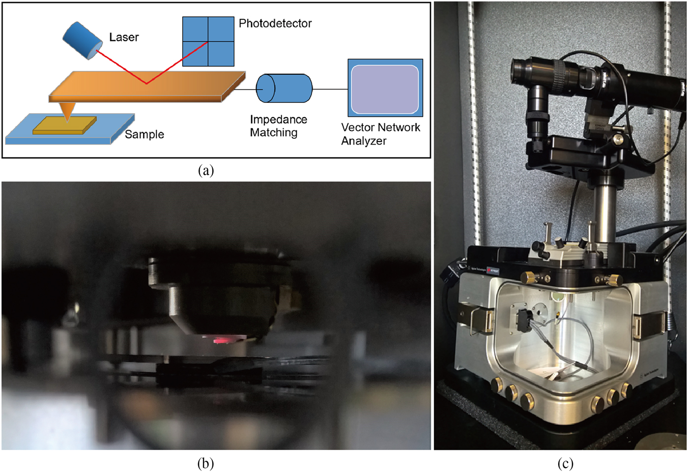
Fig. 2. (a) Schematic, (b) nose cone, and (c) stage of the present SMM setup.
Results and discussion
Figure 3 shows images formed simultaneously by AFM and SMM of 190 nm-wide bare aluminum lines. Whether an SMM image was formed by using the magnitude or phase of S 11, it appears to have comparable contrast and sharpness to that of AFM. In reality, the SNR of SMM is not as good as that of AFM due to weak SMM signals. For example, in the present case, the contrast in S 11 magnitude and phase are on the order of 0.01 dB (10 mdB) and 0.1°, respectively, comparable to that previously reported [Reference You, Ahn, Obeng and Kopanski3].
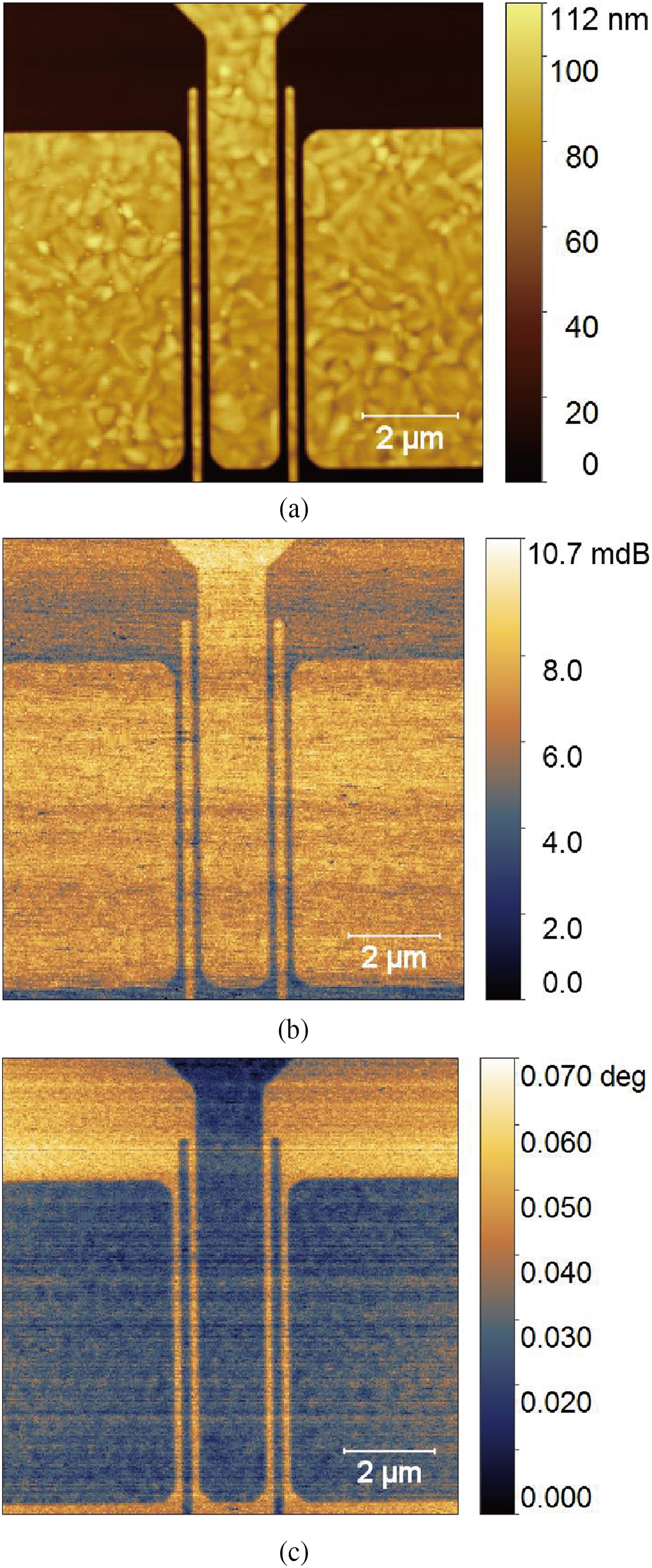
Fig. 3. Simultaneous (a) AFM, (b) SMM magnitude, (c) SMM phase images of 190 nm-wide bare aluminum lines.
Figures 4(a) and 4(b) show SMM magnitude images of 390 nm-wide bare and buried aluminum lines, respectively. It can be seen that, even when buried under 20 nm Al2O3, the lines are clearly discernable. Figure 4(c) shows that based on lateral scans across the middle of the image, bare and buried lines have comparable sharpness of approximately 70 nm. In fact, by averaging all linear scans across the lines, the sharpness was 69 ± 7 nm for bare lines and 70 ± 13 nm for buried lines. The present sharpness is comparable but not necessarily better than that of [Reference You, Ahn, Obeng and Kopanski3], because [Reference You, Ahn, Obeng and Kopanski3] buries the lines under a thicker oxide. Figure 4(c) shows also that the difference in contrast (signal magnitude) between buried lines and oxide is approximately half of that between bare lines and oxide. Had the oxide thickness not been known, it could have been estimated from the amount of the contrast degradation with the known dielectric constant of the oxide.
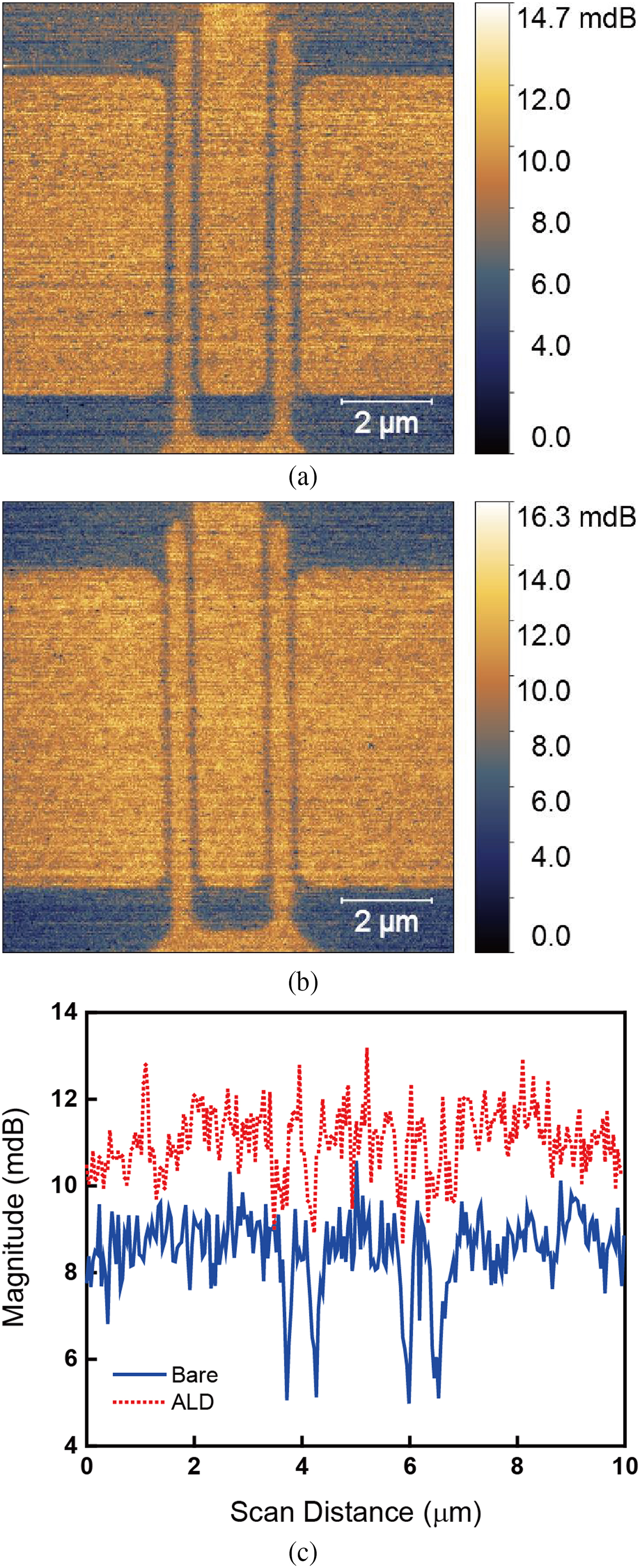
Fig. 4. SMM magnitude images of 390 nm-wide (a) bare and (b) buried aluminum lines. (c) Linear scans across both bare (—) and buried (- - -) lines.
Figure 4(c) shows that with a weaker signal, SNR is correspondingly worse for buried lines. SNR can be improved by averaging across adjacent linear scans, as will be illustrated for the scans in water. SNR may also be improved by averaging repeated scans or measurements (by VNA) at the expense of scan rate. Although presently the images formed by the S 11 magnitude and phase are of comparable quality, this is not always the case. Depending on the detailed SMM working conditions, one can be significantly better than the other. For example, for different tips, samples, tip–sample distances, and ambient conditions, the resonant frequency can shift as will be illustrated for the case in water. The change of frequency can in turn change the loss and electrical length of the transmission line, and, hence, the magnitude and phase of S 11.
As mentioned earlier, water was used to simulate high-k dielectric. Figure 5 shows the SMM phase image and linear scan over a 390 nm-wide bare line in water. It can be seen that although the line is still discernable, the signal and noise become comparable making it difficult to define sharpness from a single linear scan. However, the SNR can be significantly improved just by averaging a few adjacent scans as shown in Fig. 5(b). Statistically, a sharpness of 69 ± 13 nm was obtained, which is comparable to the cases without water. This is apparently an order-of-magnitude improvement over the 700 nm sharpness we reported in [Reference Jin, Xiong, Marstell, Strandwitz, Hwang, Farina, Göritz, Wietstruck and Kaynak4].
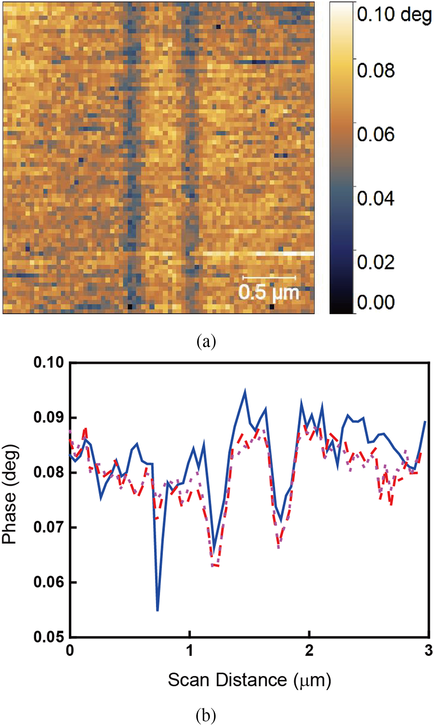
Fig. 5. SMM phase (a) image and (b) linear scans across an area of 3 µm × 3 µm (70 × 70 pixels) over a 390 nm-wide buried aluminum lines in water. In (b), averages across 6 (- - -) and 10 (…) adjacent lateral scans approximately 40 nm apart are shown for comparison with a typical single scan (―).
The sharpness improvement over [Reference Jin, Xiong, Marstell, Strandwitz, Hwang, Farina, Göritz, Wietstruck and Kaynak4] is mainly due to the difference in the parasitic capacitance between the probe body (cantilever) and the sample. Figure 6 illustrates schematically the capacitive interaction when a probe traverses an aluminum line embedded in silicon dioxide. In general, the capacitance can be divided into two parts, a sensing capacitance between the probe tip and the sample and a parasitic capacitance between the probe cantilever and the sample. Usually, with the tip in intimate contact with the sample and the cantilever suspended 80 µm in air above the sample, the parasitic capacitance is relatively small even though the cantilever is much larger than the tip. However, with the air replaced by water, the parasitic capacitance increases drastically. This parasitic capacitance not only overwhelms the sensing capacitance, but also remains constant so long as the cantilever completely overlaps a wide aluminum line such as in [Reference Jin, Xiong, Marstell, Strandwitz, Hwang, Farina, Göritz, Wietstruck and Kaynak4] (Fig. 6(b)). In this case, the line is effectively being probed by the large (400 µm × 60 µm) cantilever instead of the sharp tip, which explains why the sharpness is approximately 600 nm in [Reference Jin, Xiong, Marstell, Strandwitz, Hwang, Farina, Göritz, Wietstruck and Kaynak4], much larger than the tip radius of 20 nm. In comparison, when the probe traverses a narrow line (Fig. 6(a)), both the sensing and parasitic capacitances change readily, resulting in a sharpness of 70 nm, which is not much larger than the tip diameter. Thus, counterintuitively, in water it is more difficult to probe a large feature than a fine feature due the large parasitic capacitance with the cantilever. This parasitic capacitance can be minimized by more complete shielding of the microwave signal path all the way through the cantilever such as in a strip-line configuration [Reference Lai, Kundhikanjana, Kelly and Shen7].

Fig. 6. Schematic illustration of the capacitive interaction when an SMM probe traverses (a) narrow and (b) wide aluminum lines embedded in silicon dioxide.
For narrow lines, although water degrades the SNR, the sharpness remains approximately 70 nm as in air. This is very encouraging because it implies that SMM can also be used to non-invasively probe the internal structure of a live biological cell that needs to be kept in an aqueous solution as suggested by [Reference Tuca, Gramse, Kasper, Brinciotti, Oh, Campagnaro, Badino, Hinterdorfer and Kienberger8]. However, SMM of live biological samples presents additional challenges due to their soft and moving nature which need further development.
The present SMM image in water was obtained at 7.865 GHz instead of the typical 5.371 GHz. This is because the SMM uses an impedance matching network that works only at certain resonance frequencies. The resonance frequency shifted when the probe and the chip were immersed in water as shown in Fig. 7.
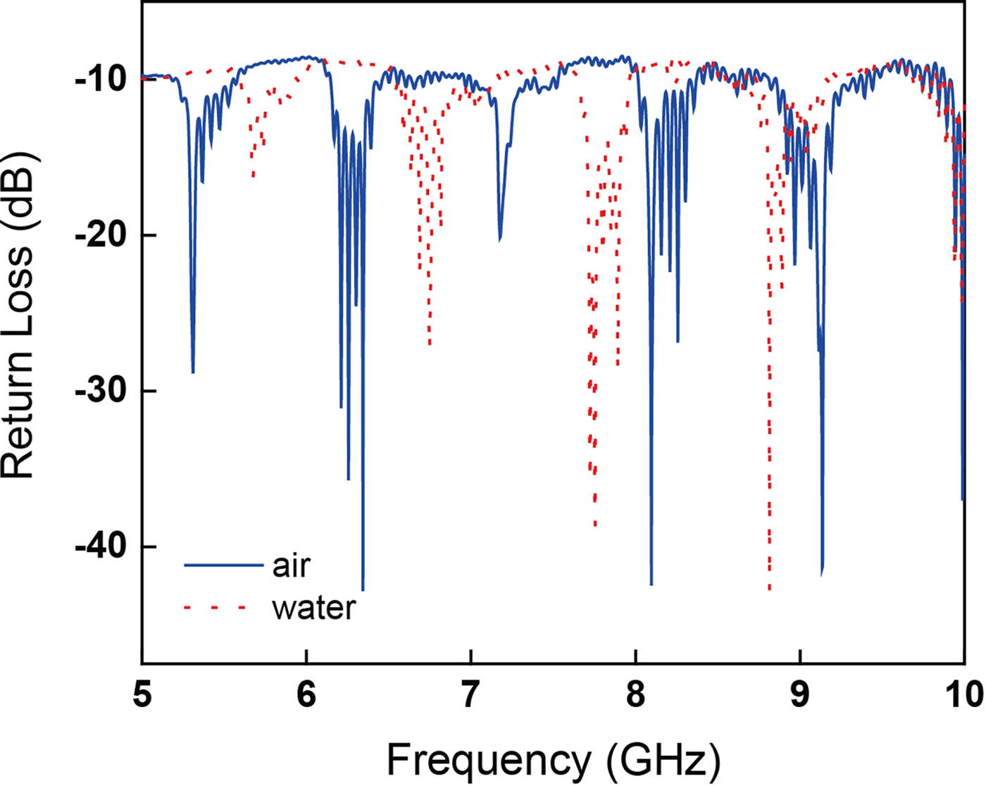
Fig. 7. Magnitude of reflection coefficient |S 11| (after subtracting the 30 dB amplification factor) from an SMM probe in air (—) and water (….) without touching any sample.
Conclusion
SMM was successfully used to image CMOS interconnect lines as narrow as 190 nm and buried under Al2O3 or water. Although water degraded the SNR significantly, it did not degrade the image sharpness. The sharpness remains approximately 70 nm in all cases. These results imply that SMM can be a promising technique for non-destructive nano-characterization of both CMOS interconnects buried under oxide and live biological samples immersed in water. However, quantitative characterization of the electrical properties of the samples awaits further development.
Acknowledgement
The project depicted is sponsored in part by the US Department of Defense, Army Research Laboratory under Grant No. W911NF-14-1-0665 and W911NF-17-1-0090, as well as Air Force Office of Scientific Research under Grant No. FA9550-16-1-0475.
 Xin Jin received the B.S. degree in Optical Science and Engineering from Fudan University, Shanghai, China in 2015. He is currently a Ph.D. student in electrical engineering at Lehigh University, Bethlehem, PA, USA. In 2016, he was a visiting Ph.D. student in Marche Polytechnic University, Ancona, Italy. He is currently involved in researches on the design and applications of scanning microwave microscope on both semiconductor devices and biological samples.
 Kuanchen Xiong received the B.E. degree in Electronic Science and Technology from Southeast University, Nanjing, China in 2015. He then joined the research group of Professor James C. M. Hwang at the Department of Electrical and Computer Engineering, Lehigh University. His current research interest focuses on 2D semiconducting materials, CMOS-compatible processes, and nano-electronic devices.
 Roderick Marstell received his B.S. and M.S. degrees from California Polytechnic State University at San Luis Obispo in 2013. He is currently a Ph.D. candidate at Lehigh University in Dr. Nicholas Strandwitz's group. His research is focused on understanding the interdependence of Schottky barrier height and electrostatic charges in atomic-layer deposited oxides.
 Nicholas C. Strandwitz joined the Lehigh University faculty in January 2013. He completed his B.S. in Engineering Science at the Pennsylvania State University in 2004. He then earned his Ph.D. from the Materials Department at the University of California, Santa Barbara with Professor Galen D. Stucky. He then conducted postdoctoral work at California Institute of Technology working with Professor Nathan S. Lewis. His research interests include new chemistries and techniques in atomic-layer deposition and interfacial electronic properties between semiconductors and metal oxides.
 James C. M. Hwang received the B.S. degree in Physics from the National Taiwan University, Taipei, Taiwan in 1970, and the M.S. and Ph.D. degrees in Materials Science and Engineering from Cornell University, Ithaca, New York, in 1976 and 1978, respectively. Since 1988, he has been Professor of Electrical Engineering and Director of Compound Semiconductor Technology Laboratory at Lehigh University, Bethlehem, Pennsylvania. Prior to that, he spent 12 years at IBM, AT&T, GE, and GAIN. He cofounded GAIN and QED; the latter became a public company (IQE). His current research interests include scanning microwave microscopy, two-dimensional atomic-layered materials and devices, and microwave characterization of individual biological cells.
 Marco Farina received the M.S. degree in 1990 and the Ph.D. degree in 1995, both in Electronic Engineering from the University of Ancona, Italy. He is currently Professor of electromagnetics at the Marche Polytechnic University, Ancona, Italy. He is a Senior Member of IEEE and a Technical Committee Member of the IEEE MTT Society TC-25 RF-Nanotechnology. He authored the electromagnetic simulation software EM3DS, currently used by a number of institutions and embedded in the National Instruments tool Microwave Office. Dr. Farina designed and realized a hybrid scanning tunneling microscope/scanning microwave microscope. His research interests include electromagnetic modeling of passive and active structures, scanning probe microscopy, nanotechnology and measurement techniques.
 Alexander Göritz received the Dipl.-Ing. degree in Electrical Engineering (microelectronics-semiconductor technology) from the Technical University Dresden, Germany, in 2011. In 2012, he joined the Technology Department of IHP Microelectronics, Frankfurt (Oder), Germany and started working on the development of micro-electromechanical systems (MEMS) with thin-film wafer-level encapsulation for mm-wave applications. He applied and optimized the HF vapor-phase-etching process to release the finished MEMS devices. Since 2014 he has been involved in the creation and application of back-end-of-line (BEOL) processes to realize cost-efficient passive devices.
 Matthias Wietstruck received his diploma in Microsystems Technology in 2009. Since 2010, he has been with IHP Microelectronics, Frankfurt (Oder), Germany. Since 2015 he is leading the group “Heterointegration of Devices and Technologies” as part of the research program “Technology for wireless and broadband communication”. His research interest is in the field of monolithic and heterogeneous integration of millimeter-wave BiCMOS RF-MEMS, through-silicon vias, temporary and permanent wafer bonding applications, and BiCMOS embedded microfluidics.
 Mehmet Kaynak received the B.S. degree from the Electronics and Communication Engineering Department of Istanbul Technical University, Turkey in 2004, the M.S degree from the Microelectronic Program of Sabanci University, Istanbul, Turkey in 2006, and the Ph.D. degree from Technical University of Berlin, Germany in 2014. He joined the technology group of IHP Microelectronics, Frankfurt (Oder), Germany in 2008. From 2008 to 2015, he led the MEMS development at IHP. Since 2015, he is Head, Technology Department at IHP. He is an Adjunct Professor at Sabanci University.


