Introduction
In recent years, silicon–germanium (SiGe) technology proved high performances for components with high monolithic integration [Reference Cressler1,Reference Russer2], increased speed with low-power consumption. Continuous progress in this technology renders possible large spectrum of applications from radio frequency (RF), microwave to THz [Reference Wane3], which used to be implemented using III−V compound semiconductors (e.g. GaAs-based technologies) (Fig. 1).
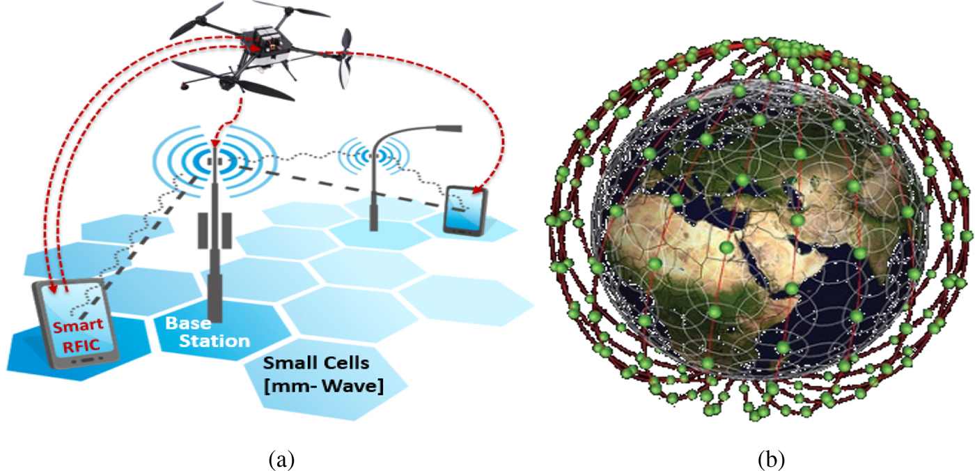
Fig. 1. Use of UAV systems in 5 G as a relay between macro-cell base station and user equipment (a). Low earth orbit (LEO) in the perspectives of Internet Everywhere (b).
In space and defense applications, in addition to standard trade-offs between application driving parameters such as noise, power, linearity, thermal dissipation, environment conditions (e.g. irradiation, harsh thermal variations) put strong constraints on system-level performances in terms of robustness and variability. Thus, analysis, characterization, and predictive [Reference Boguszewski4] modeling of environmental effects on constitutive system-level components/function blocks is of paramount importance.
In the prior art, investigated typical devices encompass both active (MOS and heterojunction bipolar transistors, diodes) and passive samples (transmission lines, interconnects) [Reference Cressler5, Reference Andrews6]. When heavy charged particles such as protons traverse a structure with medium energy (from 20 MeV to several hundreds of MeV), particles induce both ionization and atomic displacement (non-ionizing) effects. Then along the path of the incident proton in the material, both ionizing and non-ionizing energy loss modify the oxide/silicon interface (total ionizing dose, TID effect), the junctions, and the silicon bulk properties as displacement damage dose (DDD) effects. Experimental results and simulations reported in the literature have demonstrated that SiGe devices are tolerant to permanent degradation induced by radiation for both TID for several MRad and DDD effects [Reference Wane7–Reference Cressler10]. Nevertheless, most of previously published research studies focused on specific device-oriented modeling and characterization, where interactions and couplings between neighboring elements (components, function blocks, subsystems) are generally not addressed. Furthermore, very limited attention is devoted to the effects of extreme environmental conditions on electromagnetically radiating structures such as antennas, which will enable important functionalities such as MIMO, beamforming, and beamsteering [Reference Wane7]. In this contribution, based on representative structures for linear (passive interconnects), non-linear (low-noise amplifier (LNA)), and electromagnetically radiating elements (antennas), experimental analysis assessing the impact of extreme environmental conditions on the performances of SiGe:C-integrated circuits and systems is proposed in the perspectives of space–defense and emerging 5G mission-critical applications. The contribution is built around two main sections. Section “Experiments in aggressive proton-radiation environmental conditions” describes experiments on passive and active samples in aggressive proton-radiation environments. The third section reports reliability modeling analysis of non-linear components (LNAs). Predictive modeling of degradation effects using in-house tooling solution is compared with the experiments demonstrating satisfactory agreement.
Experiments in aggressive proton-radiation environmental conditions
Designed SiGe BiCMOS passive and active samples were irradiated with monoenergetic (50 and 80 MeV) proton facilities at Kernfysisch Versneller Instituut (KVI). A master sample is used as a reference. Fluencies range from 5 × 10¹¹ to 1013 p/cm2 with a proton flux of 3 × 10⁸ p/cm2 for lower fluencies and 3 × 10⁹ p/cm2 for the higher one. Dosimetry of irradiations indicated an accuracy of ±10% for the fluency and ±5% for the proton energy. Two samples were exposed to 53 krad from a Cobalt-60 source at 650 rad/h. Figure 2 gives the equivalent fluencies of 80 MeV protons versus aluminum-shield thickness. These curves are calculated for eight typical space missions ranging from low earth orbits to the GEO orbit.
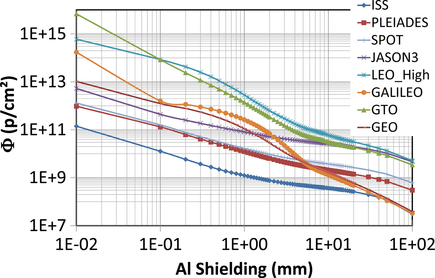
Fig. 2. Equivalent 80 MeV monoenergetic protons fluencies versus aluminum shield thickness for eight typical spatial missions. These fluencies are given for 1-year mission's durations.
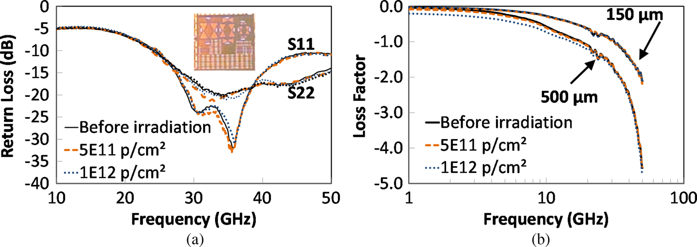
The effect of the galactic cosmic rays is neglected because their flux is too weak to induce a significant effect compared with the protons contribution. For the radiation belts models, we use the NASA-Aerospace AE8 and AP8 models in worst-case conditions (i.e. the AE8Max and AP8Min ones). For the mean solar protons model, we use the NASA ESP model with the confidence level set to 85% and we consider that all the missions are done in active period. The mission duration is 1 year for all curves. Figure 4 shows the loss factor of two mm-wave transmission lines (150 and 500 µm long, respectively) and return loss bowtie of coupled antennas (Fig. 3) that were irradiated with protons. The loss factor illustrates the various loss sources (conductive, dielectric, and electromagnetic radiative losses) without respect to impedance mismatch (since measured CPS lines characteristic impedance is not 50 Ω) and is expressed as:
 $$F_{loss} = 10 \times {\rm log}(\left \vert {S_{11}} \right \vert ^2 + \left \vert {S_{21}} \right \vert ^2).$$
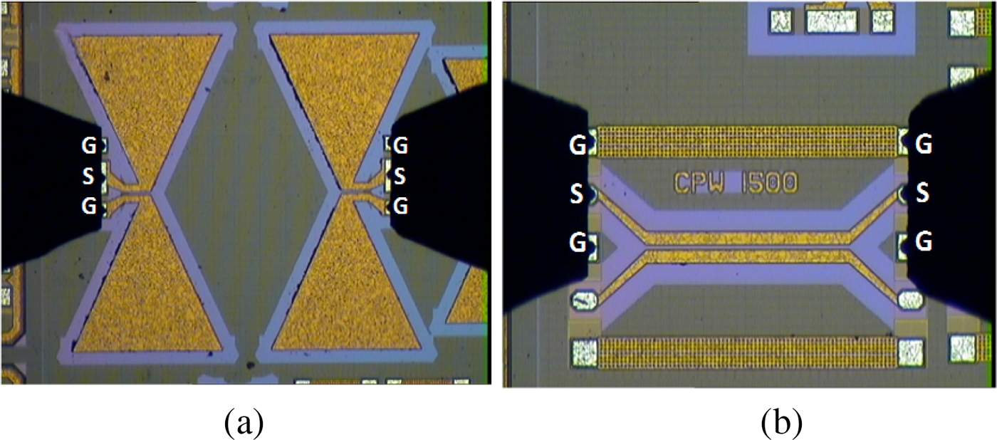
Fig. 3. Photomicrograph of the planar bowtie antenna (a) and the integrated CPS transmission line structures (b).

Fig. 4. Return loss of two bowtie slot antennas with various circuitry environments. Inset the photograph of the circuitry. Loss factor measured for two CPW lengths (100 and 500 µm) versus frequency.
As depicted in Fig. 4, for a 1012 p/cm2 irradiation, a 0.2 dB drop in the loss factor of the 500 µm long line is observed below the Ku frequency band. Such decrease is significantly higher than the measurement accuracy limit due to the variability in the RF probe contact resistance. It is observed that backend metal resistivity is slightly impacted by proton radiation; this variation may suggest a radiation-dependent decrease in silicon substrate resistivity.
Modeling and experimental analysis of active SiGe BiCMOS LNA under electrical RF stress
For this discussion, we use an in-house reliability simulation tool that contains modules of all known degradation mechanism models in bipolar and MOS devices. Supported degradation models, based on DC-accelerated stress conditions, are applied to the compact model of transistors introducing parameters shift over time.
The physical degradation phenomena in bipolar devices have been divided into two mechanisms:
• Mixed mode (MM) occurs when the device is simultaneously polarized at very high current and high base-collector bias in order to achieve speed performance [Reference Zhang11]. The MM mechanism results in an increase in the base current I b due to an increase in the interface traps in the emitter–base (EB) spacer and the shallow-trench isolation region.
The I b MM degradation model, as a function of stress conditions, is given by (2):
(2)where: t: aging time; A e, P e: effective area and perimeter; n, b and E a: constants depend on the technology. $$\eqalign{\Delta I_b = & \left( {A_E + P_E} \right)t_{stress}^n e^{\displaystyle{{ - \alpha} \over {V_{cb\_stress}\; \;}}} \left( {e^{\left( {V_{be\_stress}/((K_B\; \; T_{stress})/q)} \right)} - 1} \right)^b \cr & \left( {e^{V_{be\_read}/(m(K_B\; \; T_{stress})/q)} - 1} \right)e^{\left( { - E_a/(m(K_B\; \Delta T_{read})/q)} \right)},} $$
Figure 5 shows simulation results of base current I b and current gain degradation after MM stress, in function of collector–base stress voltage. The curves show that the degradation of current gain becomes significant from 3.3 V. Simulation results are compared with correspondent degradation model. The curves exhibit a very good matching which attest the reliability simulation tool accuracy.
• Reverse base emitter bias (RVBE) occurs when the EB junction is reverse-biased near breakdown voltages [Reference Neugroschel, Sah and Carroll12]. Also, the RVBE degradation results in an increase in the base current I b due to interface trap generation at the EB junction perimeter. Equation (3) presents the RVBE DC degradation model:
(3)$$\eqalign{\Delta I_b = & P_E\; t_{stress}^n e^{\displaystyle{{ - \alpha} \over {V_{eb\_stress}\; \;}}} \left( {(1 - c) + c.e^{\left( { - E_a/((K_B\; \; T_{stress})/q)} \right)}} \right) \cr & \left( {e^{\left( {V_{be\_read}/(m(K_B\; \; T_{stress})/q)} \right)} - 1} \right)e^{\left( { - V_g/(m(K_B\; \Delta T_{read})/q)} \right)},} $$where: t, aging time; P e: effective perimeter; V g: band gap voltage; n, α, and E a: constants depend on the technology.
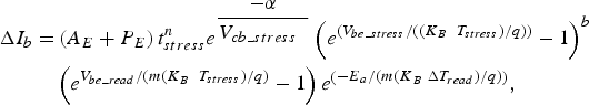

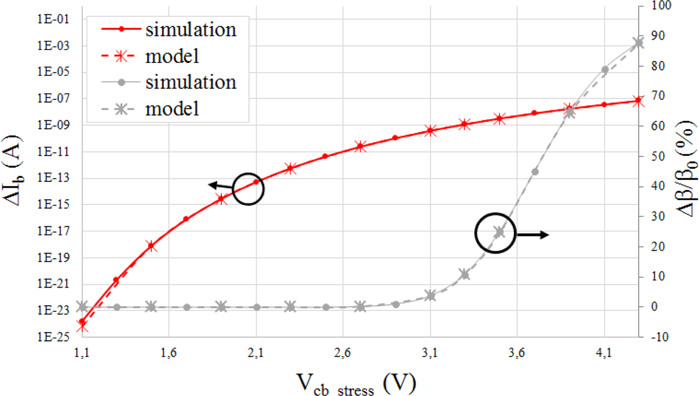
Fig. 5. Comparison of simulated ΔI b and Δβ/β as a function of V cb_stress based on MM degradation model (high-voltage SiGe NPN: after 10 years of stress at 40 °C).
To validate the implemented RVBE model in the in-house reliability simulation tool, we also compared the simulated degradation of the base current and the current gain with the model. Simulations are conducted on a SiGe NPN transistor under reverse base–emitter stress voltage. The different curves are shown in Fig. 6. They demonstrate in one hand a very good matching between both, in other words, the accuracy of the tool. On the other hand, we can conclude that the degradation of the gain current becomes significant from −1.7 V.
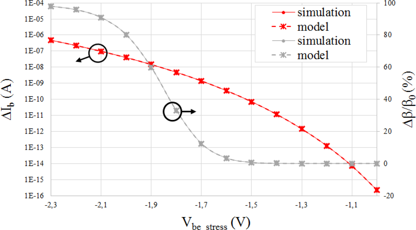
Fig. 6. Comparison of simulated ΔI b and Δβ/β as a function of V be_stress based on RVBE degradation model (high-voltage SiGe NPN: after 10 years of stress at 40 °C).
In reliability simulations, the device or the circuit is simulated in transient mode, and the aging of the modeled parameter, in this case ΔI b, is integrated over time. Subsequently, this aging is extrapolated to the stress time of interest. Therefore, the circuit could be simulated with the updated parameters.
Same degradation models are considered when the device-under-test is stressed under RF stimuli. The simulator calculates the dynamic (RF) stress damage by summing up the instantaneous damage of the transistor over a short incremental time of a quasi-static stress voltages [Reference Scholten13].
A specific attention is directed toward verifying the applicability of quasi-static-based approximations in using DC stressing data for RF stressing lifetime prediction. In the following, DC and RF stress are applied to LNAs designed for WLAN applications in order to assess the impact of aging on their RF performances. Several reliability studies have been carried out on transistors and circuits under DC stress conditions. The aim of these studies is to identify the physical origin of the degradation mechanisms and provide models describing performance shifts [Reference Cressler14,Reference Huang15]. However, the degradation of RF and mill metric circuits under RF stresses remains poorly studied and little-understood subject.
The validation of the quasi-static approximation throughout the comparison between the simulated degradation of the LNA performance, designed in 0.25 µm BiCMOS technology, and measured results permit to develop an improved design methodology, which includes reliability assessment according to the circuit's mission profile.
LNA architecture and specification
The under test LNA is shown in Fig. 7. It consists of a common source configuration using cascode transistors with feedback. This configuration is the most classical topology used in the design of LNAs.
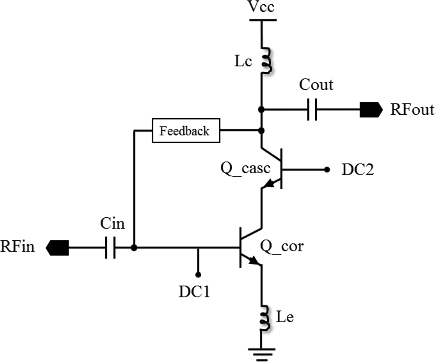
Fig. 7. LNA architecture.
LNA mission profile
The mission profile awareness aids to accurately investigate and validate the design robustness with respect to given requirements. The considered circuit under test operates from 5.15 to 5.85 GHz at a supply voltage V cc of 3.6 V.
The maximum operating temperature is assumed to vary in the range from 85 to 100 °C, and the maximum input power RF in = 7 dBm. It is designed for a term of 5 years of operation. Estimated time to failure is defined as the time to reach more than 3 dB gain loss (ΔS 21/S 21 > 25%). The noise figure (NF) increase is also considered as a failure criterion if it is higher than 3 dB (ΔNF/NF > 30%). Therefore, reliability simulations are carried out after 5 years of RF stress. Simulation results are compared with the measurements carried out based on the accelerated aging test.
RF-accelerated aging test
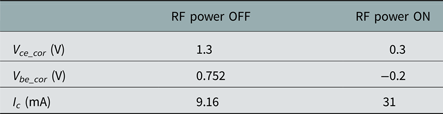
In order to accelerate the degradation of the LNA at 5.6 GHz (V cc = 3.6 V), we increase the temperature to 100 °C with an input power of 20 dBm. Although at such power level the amplifier compresses, the stress power is still under the power handling capability of the used cascode topology. When the RF stress signal is applied on the circuit, the DC drain current increases from around 9.16 to 31 mA as a consequence of the self-biasing of the LNA circuit. The evolution of the DC biasing during RF stress is presented in Table 1. The RF signals used in the stress are presented in Fig. 7 with a V cb stress voltage peak around 2.5 V and a V be stress voltage peak at −3.8 V.
Table 1. Simulated DC biasing evolution during the application of RF power
These peaks exceed the voltage limits of the used technology leading to accelerated degradation under the aforementioned MM and RVBE mechanisms (Fig. 8).
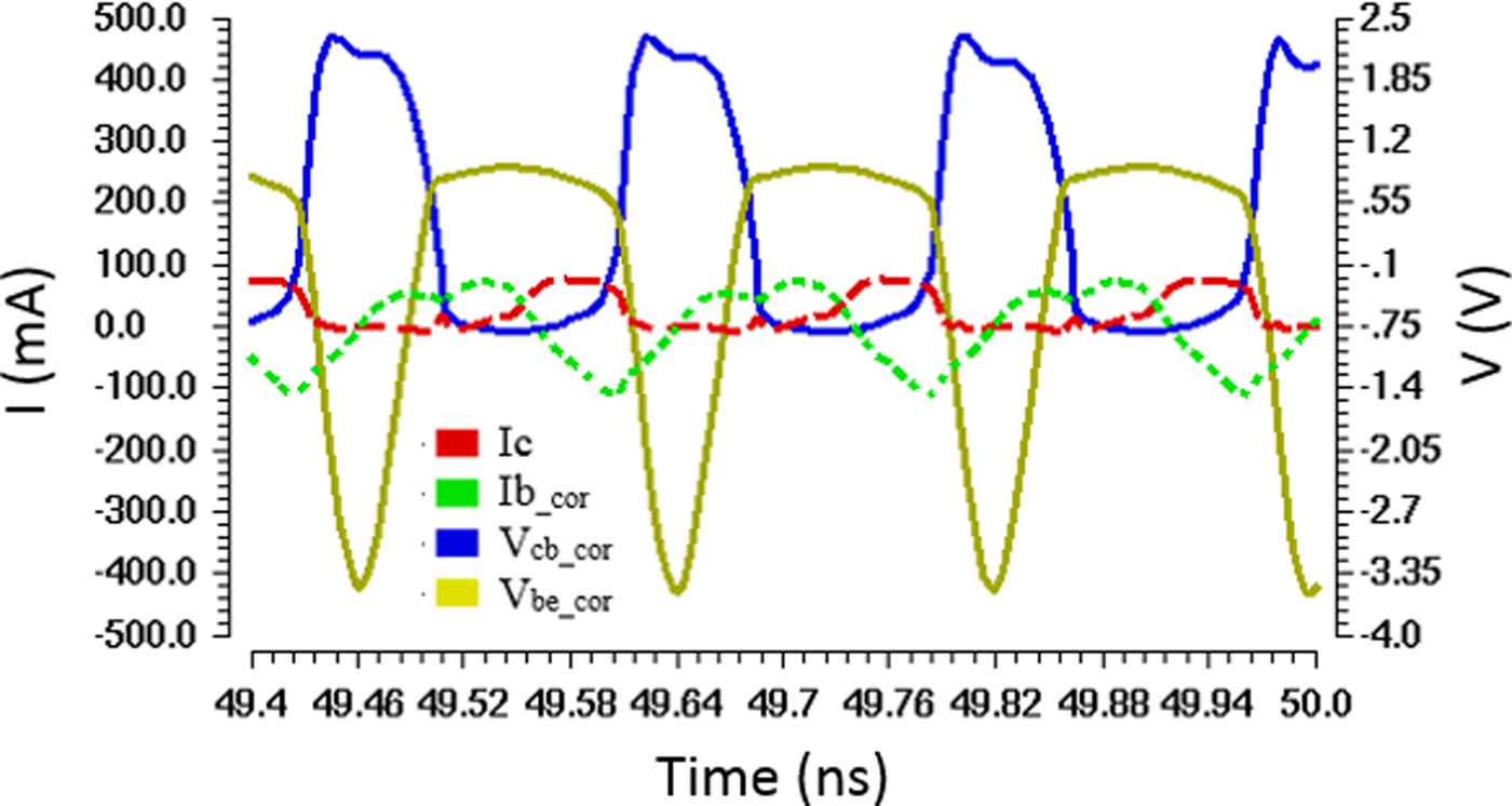
Fig. 8. AC collector–base voltage, AC base–emitter voltage, AC base current, and AC collector current of LNA during the application of RF power stress.
Experimental test-bench description
In order to assess the accuracy of the predictive simulation results, experimental accelerated aging tests are applied on the fully integrated LNA circuit reported on application board, as depicted in Fig. 9.
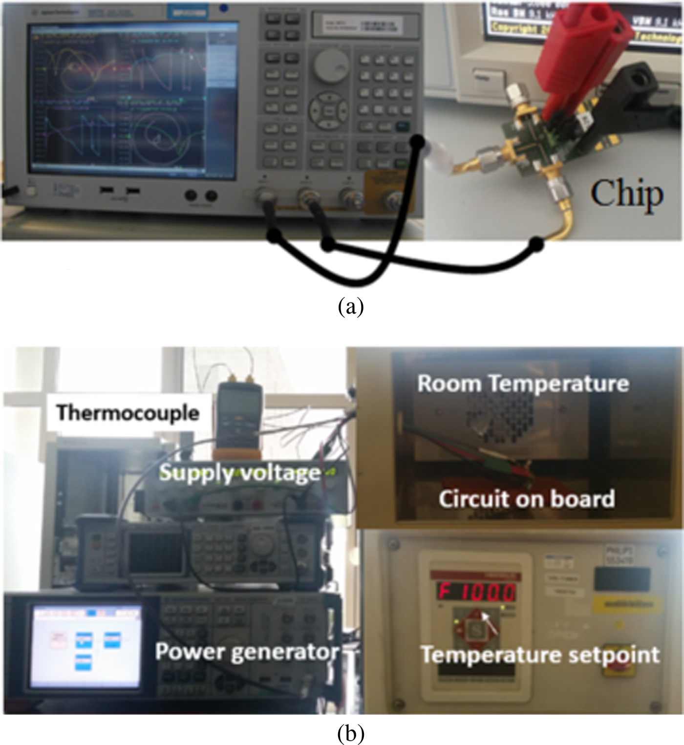
Fig. 9. Set up for RF performance measurement of the fully integrated LNA circuit reported on application board (a) and RF stress application (b).
For fair comparison between simulations and measurements de-embedding procedures are applied for properly taking into account both losses in RF transmission cables and the IC package and board parasitic. All along the stress, the evolution of the RF performances of the LNA are measured in small signal.
The NF and the correlation parameters are measured using a PNA-X instrument in a broad frequency range from 1 to 8 GHz before and after 336 h of stress. The analysis of the reliability results is based on the comparisons between RF performances before and after applying the stress stimuli.
Results and discussions
Figure 10 shows the relative variation of simulated and measured S-parameters as a function of aging time. Despite the observed degradation, the circuit did not reach the criterion of failure (in term of S 21 limits).
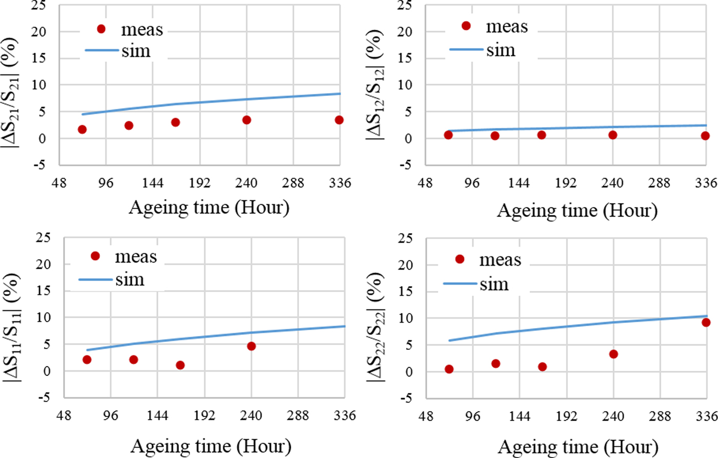
Fig. 10. Comparison between simulated and measured S-parameters degradation at 5.6 GHz after 336 h of 20 dBm stress: ΔS ii/S ii is defined as the relative degradation.
As depicted in Fig. 11, the simulated NF increases by 13.5% at 5.6 GHz after stress. Simulated results are compared with the measurements showing good agreement.
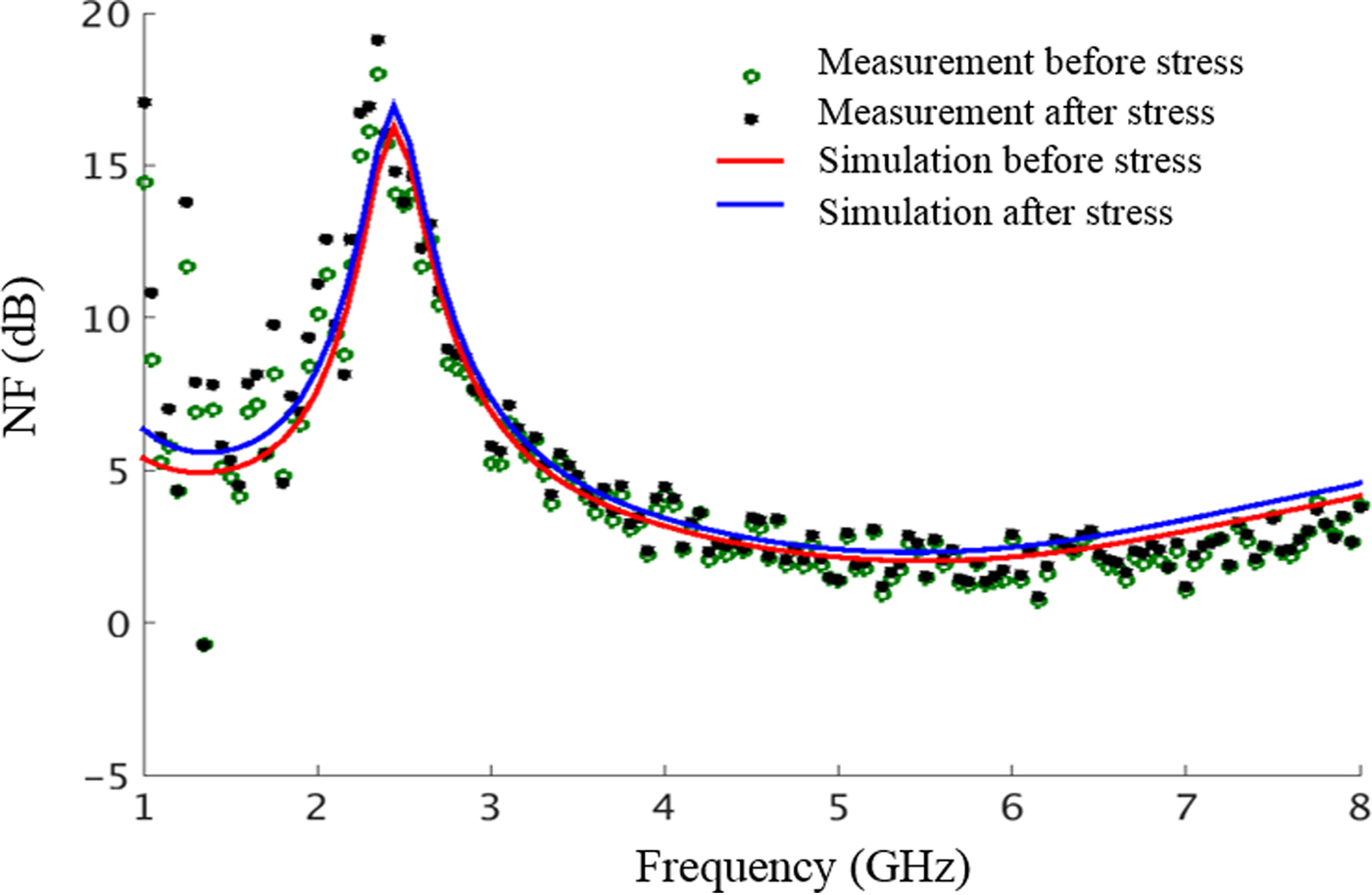
Fig. 11. Comparison between simulated and measured NF after 336 h of 20 dBm stress.
In order to identify the mechanism that is mainly determinant of Q cor degradation during RF stress, we apply the following methodology:
• First, we generate the netlist of the aged circuit by activating the two mechanisms RVBE and MM. We then simulate the gain of the LNA described by this netlist.
• Second, we deactivate one of the two mechanisms, for example, RVBE while keeping the MMD mechanism activated, and then we generate the aged netlist to simulate the LNA gain after aging.
• Finally, we redo the same thing by keeping RVBE activated without MMD mechanism.
The simulated gain of these three cases is shown in Fig. 12. As can be seen, the degradation of the LNA is mainly due to the RVBE degradation mechanism. The latter occurs in the presence of a high inverse base–emitter voltage. The MM degradation mechanism has no significant effect on gain shift, because the resulting collector–base voltage is not high enough to trigger it and thus cause degradation.
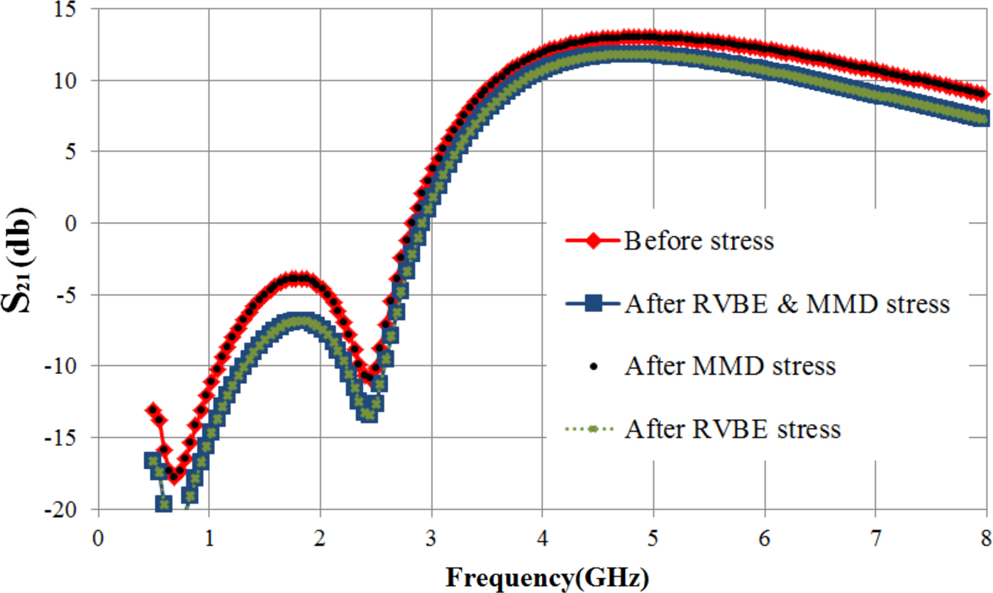
Fig. 12. Simulation of the contribution of MM and RVBE degradation mechanisms to the LNA gain shift after 336 h of 20 dBm stress.
We are now interested in the variation of the transistors small-signal model parameters (Fig. 13) as a function of the stress RF power. The aim of this study is to determine the sensitivity of the LNA gain to the degradation of these parameters.
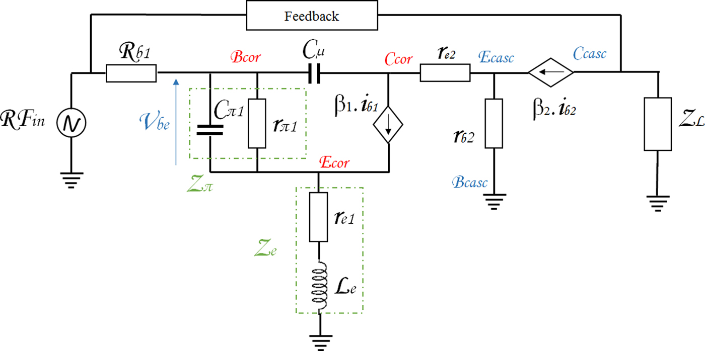
Fig. 13. Small-signal model of cascode LNA with feedback.
We varied the RF power from 15 to 21 dBm @ 5.6 GHz. Then, we extracted the relative degradations of the different small-signal parameters after 336 h of stress.
The studied parameters of the core transistor are: the resistance and the base–emitter capacitance (r π and c π), the transconductance g m1, the emitter resistance r e1, and the Miller capacitance C μ. Concerning the cascode transistor, we focused on its transconductance g m2 and its emitter resistance r e2.
The extraction, in relative value ΔX/X, of these different parameters as a function of the stress power is presented in Fig. 14. The negative values correspond to a decrease in the parameter and the positive variation in an increase.
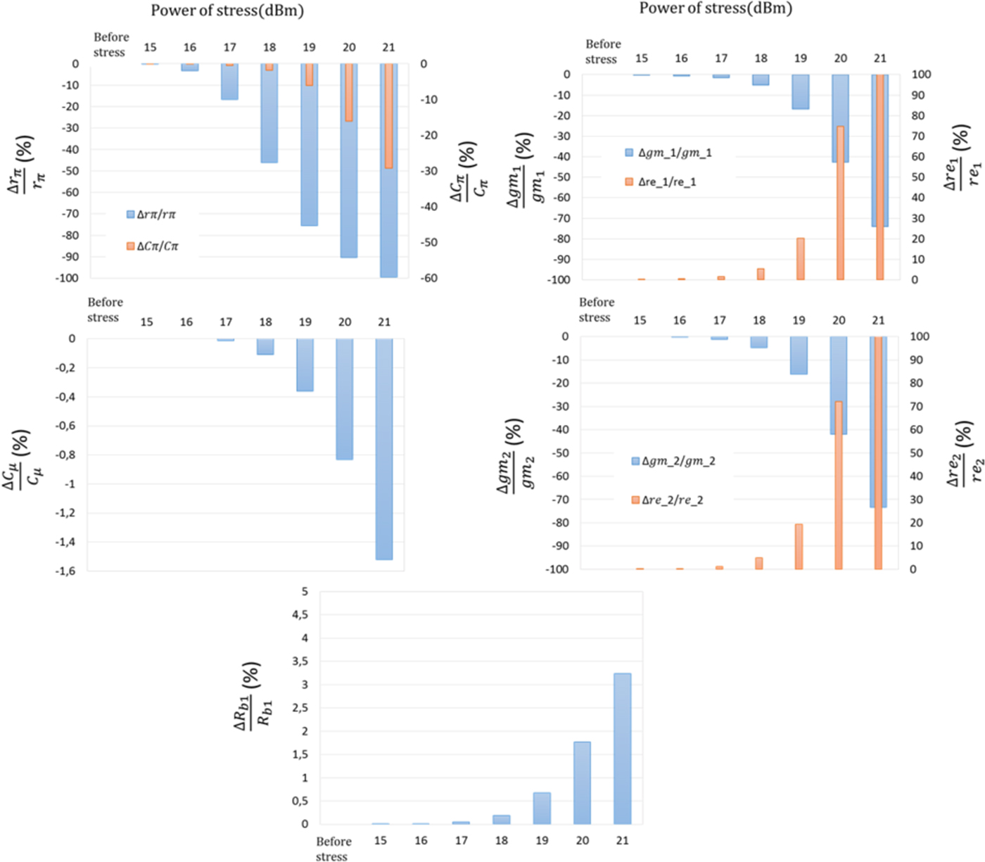
Fig. 14. LNA small-signal parameters degradation after 336 h of stress in function of RF input stress power.
Up to 16 dBm, no degradation is observed on the different parameters. From 19 dBm, degradation begins to be noticeable, then very significant, for a stress power of 21 dBm. Reliability measurement results, presented above in Figs 10 and 11, are conducted under 20 dBm of stress RF power after doing to these simulation analyses.
These simulations show that the transconductances of the two transistors g m1 and g m2, extracted at the operating points of the LNA, decreased by 42% at 20 dBm and by 75% at 21 dBm. This represents the main cause of the gain degradation. At 20 dBm, the degradation of r π, r e1, and r e2 reached 90%. However, the degradation of the Miller capacitance C μ and the basic resistance r b1 is insignificant.
These variations in small-signal parameters, mainly due to RVBE mechanism, made the overall degradation of gain and NF.
The source of the LNA noise is mainly the resistance R b1, the current of the base I b, and therefore the current of the collector I c of the core transistor.
The increase of the NF is mainly due to the rise of the I b1 current and the R b1 resistance. Under a stress of 20 dBm, I b moved from approximately 4 to 40 µA (Fig. 15) and the resistance increases by 1.8% of its initial value (Fig. 14).
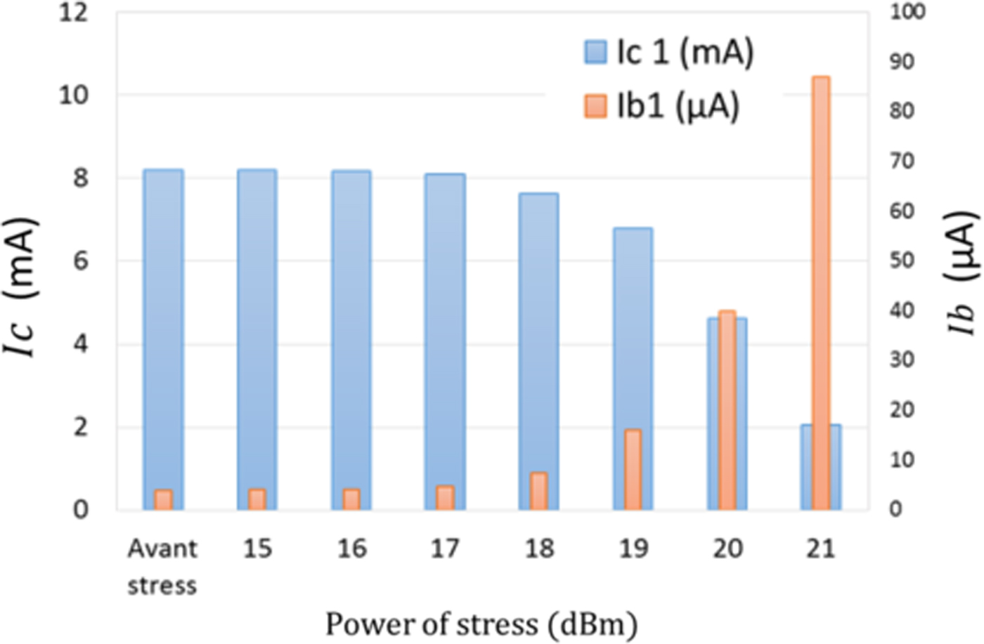
Fig. 15. DC currents after 336 h of stress in the function of RF input stress power.
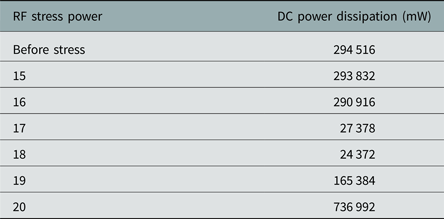
The decrease of the drain current after stress leads to DC power dissipation shift. Related simulation results are summarized in Table 2.
Table 2. DC power dissipation in function of RF input stress power
Design for reliability
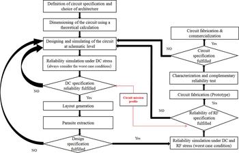
Currently, the design cycle guaranteed only the electrical performance of the integrated circuits before aging. These performances throughout product lifetime are, in general, assured by taking design margins and accelerated aging tests that come in a second complementary phase to guarantee the circuit reliability. In case of degradation, a reactive design correction is launched. This will necessarily mean a delay in placing the product on the market. To avoid this inconvenience, we propose a general design flow, which takes into account the circuit reliability improvement (Fig.16).
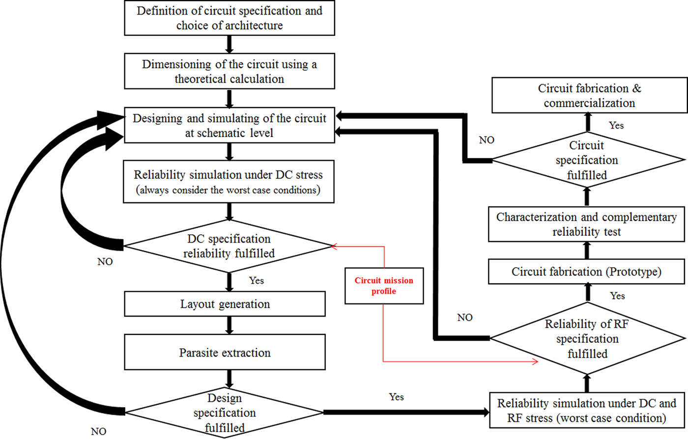
Fig. 16. Design flow aware circuit reliability: design steps illustration including reliability simulation.
Thanks to the use of reliability simulation tool, great improvement in terms of performance and reliability trade-off could be achieved. In fact, without such tool designers are obliged to take margins on design parameters according to the technology being used. To conclude, this design aware circuit reliability will be very helpful in ensuring first-time-right success target with reduced time-to-market.
Conclusion
In this paper, the impact of extreme environmental conditions on SiGe:C BiCMOS-integrated circuits is experimentally studied in the perspectives of qualifying silicon-based technology for space applications. Canonical representative structures including linear (passive interconnects/antennas) and non-linear (LNAs) are used as carriers for assessing the impact of aggressive stress conditions on their RF performances.
Predictive modeling of degradation effects using in-house tooling solution is compared with the experiments demonstrating good agreement. Ongoing work concerns the analysis of interaction mechanisms (substrate resistivity variations, couplings/interferences, and drift in DC and RF characteristics) as a function of temperature and stress power levels for assessing mission-critical profiles for emerging RF and mm-wave applications.
Acknowledgement
This work was supported in part by COST ACTION IC1407, and by the European Union's Horizon 2020 research and innovation program under grant no. 664828 (NEMF21).
 Insaf Lahbib received her Engineer diploma in Instrumentation in 2013 from the “Institut National des Sciences Appliquées et Technologies” (INSAT Tunisia) and M.Sc. degree in Electronics in 2014 from the University of Caen, France. She is actually a Ph.D. student at the Laboratory of Microelectronics and Physics of Semiconductors (LaMIPS), Caen. Her main research interests include the integrated circuits reliability.
 Sidina Wane holds a Dr.-Ing.-HDR degree in electronic circuits and systems working on chip-package-PCB co-design, co-simulation, and experimental co-verification. His main interest is in the field of power integrity, signal integrity, EMC (electromagnetic compatibility) and EMI (electromagnetic interference) in integrated circuits/systems for RF (radio frequency), mm-wave, and THz applications. In 2013, he received the HDR (Habilitation à Diriger des Recherches) diploma on the topic of “Power Integrity, Signal Integrity, EMI & EMC in Integrated Circuits and Systems: Towards Multi-Physics Energy-Oriented Approaches.” The distinguished awards bestowed on him include the Leopold Escande award together with the GEET (Génie Electrique Electronique et Télécommunications) award for his Ph.D. dissertation in 2002, the innovation award presented by the French ministry of research in 2003. He is member of the European Management Committee for COST Action 1407 relative to stochastic radiations of densely integrated circuits for emerging 5G and Internet-Of-Things systems. He is member of the French IEEE sections on Instrumentation and Microwave Theory and Techniques. He has several European and US patents on technological implementation of RF and mm-wave circuits and systems. Dr. Wane is the architect of TWF (transverse waves formulation) – a full-wave electromagnetic solver based on energy considerations suitable for RFICs (radio frequency integrated circuits) and module-based co-design and co-simulation. Dr. Wane is the founder and CEO of eV-Technologies – a high-technology company providing leading edge energy-aware tools, instrumentations and chip-package-PCB-antenna co-design solutions for RF, millimeter-waves and optical applications based on semiconductor manufacturers in Europe with partners across the world. eV-Technologies offer unified EDA & Instrumentation approach built around a comprehensive measurement platform for broadband characterization, validation and test of components, circuits and systems with loop-back to modeling and failure analysis.
 Aziz Doukkali received his Ph.D. in Electronics in 1990 from the University of Montpellier (USTL). He started with CRISMAT Laboratory until 2000 to develop superconducting materials for microelectronics. From 2000 to 2008, he worked in failure analysis field in LaMIPS Laboratory. Since 2008, he has been working on BIST activities and IC reliability.
 Dominique Lesénéchal received his Technology University degree from the I.U.T. of Caen, France, in 1983. He joined the Philips group in 1985, to be a technician in various fields of the industry during 24 years (development of LED's assembly, production of Integrated Circuits, physical failure analysis of ICs, electrical microwave characterization of components for ICs). In 2009, he joined the mixed research Laboratory of Microelectronics and Physics of Semiconductors (LaMIPS), in Caen, where he is in charge of study and development of analytical techniques and characterization of electronic systems.
 Thanh Vinh Dinh received his Master degree in Micro Nano Electronics from Joseph Fourier University, Grenoble, France, in 2010, and his Ph.D. degree in Micro Nano Electronics from the École nationale supérieure d’ingénieurs de Caen (ENSICAEN), Caen, France, in 2015. He is currently working as a Research Engineer in Electromagnetics Modeling & Simulation, and RF design at the Laboratory of Microelectronic & Physics of Semiconductor (LaMIPS), Caen, France.
 Laurent Leyssenne received his M.S. and Ph.D. degrees from the ENSEIRB/University of Bordeaux respectively in 2001 and 2009, respectively, where he designed RF ICs and amplifiers on silicon for microwave applications. From 2009 to 2011, he has been with the Research Institute in Electronic Embedded Systems in Rouen. From 2012 to 2106, he has been in charge of the development and modeling of microwave passives and antennae at the Research Laboratory of Microelectronics and Physics of Semiconductors (LaMIPS) in Caen.
 Rosine Coq Germanicus was born in Schoelcher, Martinique, France. She received her Ph.D. degree in 2002 from the University of Montpellier 2 (France) with CNES and ALCATEL SPACE in radiation effects on optoelectronics device for space reliability. Since 2003, she is an Associate Professor at the University of Caen (IUT-CRISMAT). Her research interests include radiation effect for devices space qualification and near field probe microscopy with particular emphasis on local electrical characterizations of semiconductor devices for micro and nano-electronics reliability in high integrated process.
 Françoise Bezerra received her degree in Electronic Engineering from the French Civil Aviation National School in 1991. She joined the CNES, the French Space Agency, in 1992 as a quality insurance engineer in charge of microprocessors, ASICs and FPGAs. Since 2008, she is Principal Investigator of the CARMEN/MEX instrument that studies radiation effects on electronic devices on board of JASON2, SAC-D, and JASON3 satellites. Finally, she is a Radiation Safety Officer for the CNES Toulouse and is involved in the local Radiation Protection Community (Vice-President of the RAMIP Association). Françoise BEZERRA has co-authored more than 70 papers in radiation testing or in-flight experiments and has also chaired various sessions at RADECS conferences. In 2017, she entered the RADECS Association Council Board, in charge of workshops. She will be the RADECS 2019 conference technical chair.
 Guy Rolland received the Engineers degree in Electronics in 1977. In 1978, he was with the Physic-Electronic Department, CNES (the French Space Agency), Toulouse, France. Until 1988, he was responsible for the CCD characterization laboratory and for the theoretical modeling of optoelectronic components. He was involved in numerous earth observation and scientific projects. From 1989 to 1997, he was particularly involved in process and device simulations applied to optoelectronics. He is today responsible for researches in the field of space radiation environment modeling and the effect of radiation on optoelectronic components.
 Patrick Martin received the B.E. and M.E. degrees from Caen University and Ph.D. from Rouen University, France, in 1981, 1983, and 1991, respectively. His first areas of research interest were the development of data flow architectures and algorithms for real-time inspection by computer vision-assisted automatic control of quality in industrial process. He joined the LaMIPS Ensicaen, in 2004, since he works on robustness, reliability, and instrumentation for reliability of electronic devices.
 Philippe Descamps received his Ph.D. degree from the University of Lille, France, in 1992. From 1989 to 1999, he joined the research group Integrated Systems at the Institut d’Electronique, de Microélectronique et de Nanotechnologies (IEMN), Villeneuve d'Ascq, France, where he was involved in microwave research activities mainly guided by the Characterization, Simulation and Design, and by the realization of field-effect devices in centimeters and millimeters waves ranges for automotive applications and telecommunication systems. From 1999 to 2018, he has been a full Professor at the Ecole Nationale Supérieure d'Ingénieurs of Caen (ENSICAEN), France where he currently heads the mixed research Laboratory of Microelectronics and Physics of Semiconductors (LaMIPS). He is mainly involved of high frequencies Characterization, Modelization of Microwave Components, and of the design of Integrated Circuits for telecommunication applications. Since 2018, he became the Director of Research and Development and Director of IRSEEM Laboratory of the school of Engineering ESIGELEC in Rouen, France.
 Guillaume Boguszewski is the founder and CEO of CYleone. He earned a PhD in electronic & electro-magnetism from INP-Polytech, Bordeaux for embedded systems (SiP, SoC, etc.). He obtained Master of Physical Sciences from Montpellier University. His professional experience for the last 15 years include: Philips-NXP Semiconductors (Deutchland, Germany, France); NASA ECE Lab (Tucson/Phoenix, AZ, USA); Domestic National Security; and Data management (data analysis, data system engineering, and data vizualization).