


Introduction
One of the greatest revolutions in scanning transmission electron microscopy (STEM) in recent years is the development and use of fast pixelated detectors incorporating direct electron detection (DED) technology, and these are rapidly becoming a key component of the imaging system for a modern STEM. Ophus (Reference Ophus2019) has provided an excellent review of the area, and Tate et al. (Reference Tate, Purohit, Chamberlain, Nguyen, Hovden, Chang, Deb, Turgut, Heron, Schlom, Ralph, Fuchs, Shanks, Philipp, Muller and Gruner2016), Yang et al. (Reference Yang, Jones, Ryll, Simson, Soltau, Kondo, Sagawa, Banba, MacLaren and Nellist2015), and Krajnak et al. (Reference Krajnak, McGrouther, Maneuski, O'Shea and McVitie2016) have described some suitable detectors for different applications in pixelated STEM imaging. Part I (Nord et al., Reference Nord, Webster, Paton, McVitie, McGrouther, MacLaren and Paterson2020) of this work briefly discussed the general benefits of fast pixelated detectors for use in STEM and presented software solutions for their hardware control, and for the acquisition, real-time processing and visualization, and storage of data from them. An increasing number of Python packages are being developed by the electron microscopy community with capability to process four-dimensional (4D) STEM (4D-STEM) data, including HyperSpy (de la Peña et al., Reference de la Peña, Ostasevicius, Fauske, Burdet, Prestat, Jokubauskas, Nord, Sarahan, MacArthur, Johnstone, Taillon, Caron, Migunov, Furnival, Eljarrat, Mazzucco, Aarholt, Walls, Slater, Winkler, Martineau, Donval, McLeod, Hoglund, Alxneit, Hjorth, Henninen, Zagonel and Garmannslund2018), LiberTEM (Clausen et al., Reference Clausen, Weber, Caron, Nord, Müller-Caspary, Ophus, Dunin-Borkowski, Ruzaeva, Chandra, Shin and van Schyndel2019), py4DSTEM (Savitzky et al., Reference Savitzky, Zeltmann, Barnard, Brown, Henderson and Ginsburg2019, Reference Savitzky, Hughes, Zeltmann, Brown, Zhao, Pelz, Barnard, Donohue, DaCosta, Pekin, Kennedy, Janish, Schneider, Herring, Gopal, Anapolsky, Ercius, Scott, Ciston, Minor and Ophus2020), pycroscopy (Somnath et al., Reference Somnath, Smith, Laanait, Vasudevan, Ievlev, Belianinov, Lupini, Shankar, Kalinin and Jesse2019), and pyXem (Johnstone et al., Reference Johnstone, Crout, Høgås, Martineau, Smeets, Laulainen, Collins, Morzy, Prestat, Ånes, Doherty, Ostasevicius and Bergh2019).
In this present article, Part II, we discuss post-acquisition data exploration and analysis of a variety of STEM datasets acquired with a fast pixelated detector, using the fpd (fpd devs, 2015; fpd demos devs, 2018) and pixStemFootnote 1 (pixStem devs, 2015) Python libraries, with a focus on their use in mapping the structural properties of materials. These include the techniques of virtual detector imaging (Rauch & Veron, Reference Rauch and Veron2005; Gammer et al., Reference Gammer, Ozdol, Liebscher and Minor2015), higher-order Laue zone STEM (HOLZ-STEM; Huang et al., Reference Huang, Gloter, Chu, Chou, Shu, Liu, Chen and Colliex2010; Nord et al., Reference Nord, Ross, McGrouther, Barthel, Moreau, Hallsteinsen, Tybell and MacLaren2019), nanobeam electron diffraction (NBED; Béché et al., Reference Béché, Rouvière, Clément and Hartmann2009), and scanning precession electron diffraction (SPED; Vincent & Midgley, Reference Vincent and Midgley1994). Throughout, we provide examples of the application of these techniques to data recorded with a Medipix3RX hybrid counting DED detector (henceforth referred to as Medipix3) (Ballabriga et al., Reference Ballabriga, Alozy, Blaj, Campbell, Fiederle, Frojdh, Heijne, Llopart, Pichotka, Procz, Tlustos and Wong2013) mounted in STEMs with 200 kV electron sources, though the techniques and software packages discussed here extend to data from other detectors. The names of the specific functions, classes, methods, modules, and packages used in the examples given are specified in the main text or the figure captions in typewriter font.
Both of the software libraries presented are made available under the free and open source GPLv3 license, allowing transparency of the implemented algorithms, and the ability for anyone to use and to further improve upon them. The libraries themselves draw on the rich ecosystem of mature Python libraries (Oliphant, Reference Oliphant2007), including ones for optimized numerical (Oliphant, Reference Oliphant2006) and scientific (Jones et al., Reference Jones, Oliphant and Peterson2001) computing, image processing (van der Walt et al., Reference van der Walt, Schönberger, Nunez-Iglesias, Boulogne, Warner, Yager, Gouillart and Yu2014; Gouillart et al., Reference Gouillart, Nunez-Iglesias and van der Walt2016), and data visualization (Hunter, Reference Hunter2007).
The pixStem library is built upon HyperSpy and extends its capabilities to common pixelated STEM tasks, with a focus on processing HOLZ data. A key difference between the pixStem and fpd packages is that the latter library is a lower level one, similar in style to NumPy but with added classes, GUIs and plotting capabilities built-in where needed. A higher-level object-oriented interface will be added in a future version. A detailed description of every feature of the pixStem and fpd libraries can be found in the documentation and example Jupyter (Kluyver et al., Reference Kluyver, Ragan-Kelley, Pérez, Granger, Bussonnier, Frederic, Kelley, Hamrick, Grout, Corlay, Ivanov, Avila, Abdalla, Willing, Loizides and Schmidt2016) notebooks available online (fpd devs, 2015; pixStem devs, 2015; fpd demos devs, 2018) and will not be replicated here. Instead, in the following sections, we describe some of the general techniques employed by the libraries for efficient data processing, for data visualization, and the main features of the libraries for the structural characterization of materials.
The paper is organized as follows. Section “General Techniques” outlines general techniques for handling postprocessing of the large 4D-STEM datasets typically produced by fast pixelated detectors. In the section “Data visualization”, ways of visualizing the datasets are discussed. Section “Virtual detector images” covers the various methods of generating virtual images from the 4D datasets, using annular dark-field (ADF) contrast from a noncrystalline soft material as an example. In the section “Higher-order Laue zone analysis”, HOLZ-STEM data analysis is explained, which allows for the retrieval of information about the periodicity of a crystalline sample in the direction parallel to the electron beam. Lastly, general lattice image processing is discussed in the section “Lattice analysis”, with a focus on diffraction imaging. Using test data obtained in the SPED mode of acquisition (Vincent & Midgley, Reference Vincent and Midgley1994) of a custom system (MacLaren et al., Reference MacLaren, Frutos-Myro, McGrouther, McFadzean, Weiss, Cosart, Portillo, Robins, Nicolopoulos, del Busto and Skogeby2020), we demonstrate that a lattice parameter fractional precision of 6 ×10⁻⁴ is possible using a probe with a spatial resolution of 1.1 nm. This precision value is approximately 2–3× larger than the best ones reported in the literature using standard probes in a SPED mode (Rouvière et al., Reference Rouvière, Béché, Martin, Denneulin and Cooper2013) and patterned probes in standard STEM mode (Guzzinati et al., Reference Guzzinati, Ghielens, Mahr, Béché, Rosenauer, Calders and Verbeeck2019; Zeltmann et al., Reference Zeltmann, Müller, Bustillo, Savitzky, Hughes, Minor and Ophus2020).
A future Part III of this work will cover post-acquisition processing and visualization of data from fast pixelated detectors for differential phase contrast imaging.
General Techniques
The primary challenge to the post-acquisition processing of data from fast pixelated detectors is the size of the data, which can easily be much greater than the available system memory on current generation computers. For example, a spatial scan with 1k × 1k points recording data from a 512 × 512 pixel detector would occupy ~977 GB when stored in 32-bit integer format. In addition to this, in some types of processing, at least the same amount of memory is required to process the data, putting the potential memory requirements well into the terabyte range. For STEM imaging, smaller scan sizes of 256 × 256 or 512 × 512 points with a 256 × 256 pixel detector at lower bit depth are often adequate to observe the specific feature of interest. In these cases, and for 16-bit data, the memory requirements are more modest, being 8.6 and 34.4 GB (in SI units), but the problem of available system memory and efficient computation currently remains.
One solution to these issues is out-of-core processing, where the data are stored on disk and only parts of it are loaded into memory when needed. As an example, to generate a bright-field image from a STEM dataset, each reciprocal space image may be loaded one at a time from a hard drive into memory, a sum of each image performed, with the resulting single values stored in memory, and the diffraction pattern memory reused to store the next image. This is an extreme example and, in reality, multiple images may be loaded into memory at once and processed across multiple CPU cores in parallel to achieve significant performance improvements.
Out-of-core processing is termed “lazy-loading” in HyperSpy and was recently added through the use of Dask (Dask Development Team, 2016), a library which abstracts away the complexities of out-of-core processing. The pixStem library relies on HyperSpy for out-of-core processing, whereas the fpd library was implemented before out-of-core processing was available in HyperSpy and so implements its own methodology, relying on HyperSpy for Gatan Digital Micrograph file access.
The two libraries can both also process in-memory data. When processing out-of-core data on disk, there are several ways of making the data exploration and analysis more efficient. Chunking the dataset in a compressed HDF5 (The HDF Group, 1997–2018) file, as discussed in Part I (Nord et al., Reference Nord, Webster, Paton, McVitie, McGrouther, MacLaren and Paterson2020), in the scan and detector dimensions by partitioning the diffraction pattern data into several pieces, can greatly speed up data processing by both reducing the data reading and decompression time, and by reducing the in-memory array sizes. For example, if one wants to make a bright-field image by using a small virtual aperture, most of the diffraction pattern can be ignored. Without chunking the detector dimensions, each full image and, thus, the entire dataset must be read. However, when a 256 × 256 pixel diffraction pattern is partitioned into 16 × 16 chunks and the bright-field disc is located within one such chunk, only 0.39% of the dataset has to be read and processed. The use of HDF5 files for data storage brings with it many additional benefits, and these are discussed more fully in Part I (Nord et al., Reference Nord, Webster, Paton, McVitie, McGrouther, MacLaren and Paterson2020).
In both packages, reading of chunked data from disk may be aligned to the chunk size when possible to optimize read times. The size of the data read into memory can be set to be independent of the chunk size or be multiples thereof, allowing data to be processed even on systems with limited memory and processing power. Additionally, many of the algorithms in the fpd and pixStem library can be set to operate using one CPU core or, by default, to employ all available cores to process the in-memory data chunk in parallel, enabling significant speed increases over single core processing.
Binning the data is another implemented method that can increase data processing speed. Detector resolution is an important factor when considering the influence of binning on data analysis. Most fast DEDs have relatively few pixels compared to conventional CCD-based detectors and the reduction in pixel counts on rebinning can limit the ability to extract the maximum signal from the data. In many cases, however, modest rebinning can be applied without significant changes in the signal-to-noise ratio (SNR), or large rebinning can be applied to vastly increase the processing speed. If the data were recorded using a detector that has no readout noise and that counts electrons only in the pixel in which they entered the detector's sensor, then the noise would be Poissonian and, for some analyses, such as center of mass, rebinning has almost no affect on the SNR of the analysis result.
The Medipix3 detector (Ballabriga et al., Reference Ballabriga, Alozy, Blaj, Campbell, Fiederle, Frojdh, Heijne, Llopart, Pichotka, Procz, Tlustos and Wong2013) has a noise-free readout when the counting threshold is set above the level of the detector's intrinsic noise and, at electron beam energies up to 80 keV, the detector is capable of a near perfect response, counting electrons mainly in the pixel of entry (Mir et al., Reference Mir, Clough, MacInnes, Gough, Plackett, Shipsey, Sawada, MacLaren, Ballabriga, Maneuski, O'Shea, McGrouther and Kirkland2017). However, 200 keV electrons can travel long distances in the sensor and are counted by multiple pixels (McMullan et al., Reference McMullan, Cattermole, Chen, Henderson, Llopart, Summerfield, Tlustos and Faruqi2007), giving rise to a point spread function of a few pixels. This correlation modifies the noise profile of the detector from pure Poisson statistics. However, rebinning the data, even by a small extent, nullifies the correlated component of the noise, resulting in a Poissonian noise profile at the expense of lower detector resolution. While rebinning tends to have little effect on the SNR of the result of many analysis techniques, it can improve it in some cases, and the speed improvements it brings are particularly useful when performing live data processing, as discussed in Part I (Nord et al., Reference Nord, Webster, Paton, McVitie, McGrouther, MacLaren and Paterson2020), or for rapid post-acquisition assessment of the data while on the microscope.
The binning of data can also be used to reduce the dataset size to the point where it can fit in memory. For example, binning the detector dimensions of a 256 × 256 × 256 × 256 12-bit dataset by 2 along each axis reduces the size by a factor of 4 from 8.6 GB down to a more manageable 2.1 GB.
Data Visualization
Once a dataset has been acquired, it is important to be able to visualize the raw data and to be able to correlate it with the results produced from processing the dataset. The DataBrowser class of the fpd.fpd_file module allows basic GUI-based data inspection, using by default the pre-rendered sum image for navigation if one of our HDF5 files (Nord et al., Reference Nord, Webster, Paton, McVitie, McGrouther, MacLaren and Paterson2020) is supplied, and loading images on-the-fly as needed. The class can also display data from other sources, such as in-memory NumPy arrays and memory mapped files, and so it is also useful when inspecting data immediately after acquisition and before conversion of the data to the HDF5 format.
To demonstrate the DataBrowser class, we use it to display a recently published nanobeam diffraction dataset (Temple et al., Reference Temple, Almeida, Massey, Fallon, Lamb, Morley, Maccherozzi, Dhesi, McGrouther, McVitie, Moore and Marrows2018b) from a cross section of a patterned, epitaxially grown FeRh/NiAl/MgO sample (Temple et al., Reference Temple, Almeida, Massey, Fallon, Lamb, Morley, Maccherozzi, Dhesi, McGrouther, McVitie, Moore and Marrows2018a). FeRh, in its B2 structure, exhibits a tunable first-order transition at a temperature of 370 K, which is accompanied by a ferromagnetic to antiferromagnetic ordering transition (Lewis et al., Reference Lewis, Marrows and Langridge2016). These properties make FeRh of interest for a number of applications, including data storage and sensors. In the following, we present an analysis of the crystal structure, a key property in determining the magnetic ordering, using the methodology detailed later, in the section “Lattice analysis”.
The top row of Figure 1 shows the screenshots of the two GUI windows of the DataBrowser class. The navigation image in Figure 1a is a user-supplied one showing the diffraction pattern lattice parameter, k, parallel to the growth direction, as indicated by the black arrows in Figures 1a and 1b (the other annotations in Fig. 1a have been added to the GUI image for this presentation of the data). The diffraction pattern at the location in the scan marked by the bottom white square in Figure 1a is shown in Figure 1b. The displayed diffraction pattern can be selected by clicking anywhere in the navigation image or by dragging the white marker with the mouse, enabling the dataset to be examined.
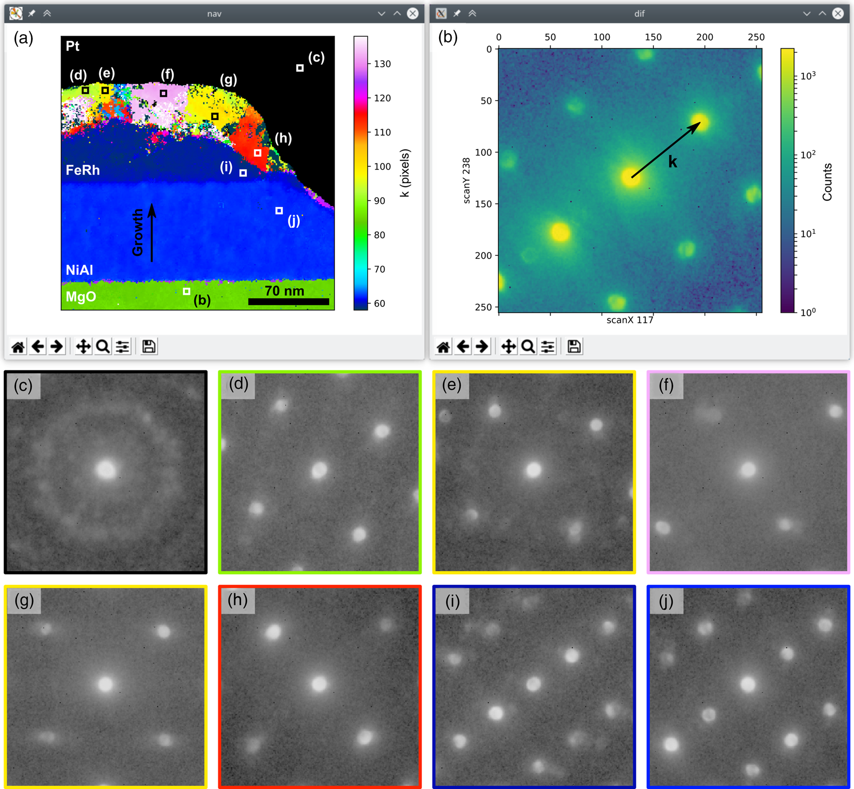
Fig. 1. Example of the DataBrowser class showing (a) a user-supplied navigation image and (b) the diffraction pattern from the scan point marked by the white square at the bottom of (a). The dataset is from an FeRh sample (Temple et al., Reference Temple, Almeida, Massey, Fallon, Lamb, Morley, Maccherozzi, Dhesi, McGrouther, McVitie, Moore and Marrows2018a, Reference Temple, Almeida, Massey, Fallon, Lamb, Morley, Maccherozzi, Dhesi, McGrouther, McVitie, Moore and Marrows2018b) and the navigation image is the diffraction pattern lattice parameter in pixels along the material layer growth direction, obtained by analyzing the data using the methodology detailed in the section “Lattice analysis”. This direction is marked by the vertical arrow in (a). The equivalent axis is marked by a similar arrow in (b) and is rotated with respect to the scan axes. The black region in (a) is from electron and ion beam deposited platinum and has been masked. All other annotations in (a) have been added to the GUI screenshots to mark the locations of the diffraction patterns shown in panels (c–j). Details of the acquisition from the referenced publications are a scan size of 256 × 256 points, a probe step size of 0.93 nm, and a semi-convergence angle <1 mrad.
The extent of the FeRh and NiAl layers and the MgO substrate are readily identifiable from regions of uniform color in the navigation image of Figure 1a. The black region in this image is from nanocrystalline platinum deposited prior to forming the cross section and has been masked in the image. Beneath the Pt layer, the top and side sections of the FeRh layer have been modified by a combination of the 1 kV Ar+ etching used in the sample patterning (Temple et al., Reference Temple, Almeida, Massey, Fallon, Lamb, Morley, Maccherozzi, Dhesi, McGrouther, McVitie, Moore and Marrows2018a) and damage done during focused ion beam cross-section preparation, creating disordered regions and grains of different FeRh structures.
While the changes in the mapped lattice parameter are indicative of different grains, the other lattice parameters must be considered when defining a grain. In Figures 1c–1j, we show diffraction patterns outlined in the same color as the regions from which they are taken in Figure 1a, with the exact single scan pixel location of each pattern marked by the equivalently labeled white or black boxes within each region. The diffraction patterns from the NiAl layer (Fig. 1j) and the epitaxial section of the FeRh layer (Fig. 1i) are both consistent with a B2 structure when viewed along the [011] direction, as reported previously (Temple et al., Reference Temple, Almeida, Massey, Fallon, Lamb, Morley, Maccherozzi, Dhesi, McGrouther, McVitie, Moore and Marrows2018a), while the MgO pattern (Fig. 1b) is consistent with the NaCl structure when viewed along the [100] zone-axis. The regions labeled in Figures 1d–1h each have a diffraction pattern consistent with a chemically disordered bcc crystal structure (Temple et al., Reference Temple, Almeida, Massey, Fallon, Lamb, Morley, Maccherozzi, Dhesi, McGrouther, McVitie, Moore and Marrows2018a), with the rotation of the crystal orientation, lattice parameter, and strain varying between regions (cf. Figs. 1e–1g). Over the imaged area, approximately half of the FeRh material is in a disordered phase.
In addition to the structural analysis of the type discussed above, the ability to inspect the 4D dataset in this manner is particularly useful in magnetic imaging, where the source, either magnetic or crystalline, of apparent beam-shifts can be interrogated by navigating the 4D dataset using a color vector magnitude image produced from the analysis [examples of vector magnitude plots of this type may be seen in Paterson et al. (Reference Paterson, Macauley, Li, Macêdo, Ferguson, Morley, Rosamond, Linfield, Marrows, Stamps and McVitie2019)]. This type of beam-shift processing will be discussed further in Part III.
More configurable plotting of data from our HDF5 files (Nord et al., Reference Nord, Webster, Paton, McVitie, McGrouther, MacLaren and Paterson2020), such as plotting along different axes, may be achieved by opening the EMD formatted (EMD authors, 2019) datasets embedded in the HDF5 file in HyperSpy (de la Peña et al., Reference de la Peña, Ostasevicius, Fauske, Burdet, Prestat, Jokubauskas, Nord, Sarahan, MacArthur, Johnstone, Taillon, Caron, Migunov, Furnival, Eljarrat, Mazzucco, Aarholt, Walls, Slater, Winkler, Martineau, Donval, McLeod, Hoglund, Alxneit, Hjorth, Henninen, Zagonel and Garmannslund2018). This can be performed with the fpd_to_hyperspy function of the fpd.fpd_file module or by loading them directly through the pixStem or HyperSpy libraries. Furthermore, the datasets may also be loaded into any custom analysis or visualization code written in Python using the fpd_to_tuple function which relies on the h5py library (Collette, Reference Collette2013), or indeed any of the many other languages supporting the HDF format (The HDF Group, 1997–2018).
Virtual Detector Images
Traditional STEM detectors are routinely used to generate image contrast by collecting the signal from electrons scattered through different angles by the sample under study, from bright-field (BF; LeBeau et al., Reference LeBeau, D'Alfonso, Findlay, Stemmer and Allen2009; MacLaren et al., Reference MacLaren, Wang, Morris, Craven, Stamps, Schaffer, Ramasse, Miao, Kalantari, Sterianou and Reaney2013), through annular bright-field (ABF; Hammel & Rose, Reference Hammel and Rose1995; Findlay et al., Reference Findlay, Shibata, Sawada, Okunishi, Kondo and Ikuhara2010) to ADF, and high-angle annular dark-field (HAADF; Pennycook & Jesson, Reference Pennycook and Jesson1991; Hartel et al., Reference Hartel, Rose and Dinges1996). However, these detectors offer a limited range of often mutually exclusive fixed collection angles at any given camera length. By using a pixelated detector, the range of scattering angles is resolved and this provides great flexibility in the both the number and range of collection angles from which images may be constructed by applying “virtual” apertures to the dataset in software (Rauch & Veron, Reference Rauch and Veron2005; Rauch & Véron, Reference Rauch and Véron2014). In addition to allowing greater insight into the sample properties, pixelated detectors have the potential benefit of being more dose efficient than segmented diode or photomultiplier tube detectors (Shibata et al., Reference Shibata, Kohno, Findlay, Sawada, Kondo and Ikuhara2010) by avoiding repeated scans when multiple collection angles are required, and also do not require the careful calibration (Jones et al., Reference Jones, Varambhia, Sawada and Nellist2018) that traditional STEM detectors do in order to minimize errors in quantitative imaging. Furthermore, when there are no de-scan coils in a system, or where they are not perfectly set up, movement of the probe position on the detector will occur; an effect that is especially apparent in large area scans. This can be corrected for in software when using a pixelated detector, whereas with fixed geometry detectors, a range of collection angles depending on the probe position would be sampled, potentially giving rise to nonintuitive or nonquantitatively-interpretable contrast in the resultant image.
In many cases, this effect is not a significant one, but when it is, the data may be corrected during HDF5 file creation (Nord et al., Reference Nord, Webster, Paton, McVitie, McGrouther, MacLaren and Paterson2020) or the data may be corrected afterwards. Multiple methods may be used to determine the direct beam position. Thresholded center of mass and edge-filtered phase correlation techniques, such as those implemented in the fpd.fpd_processing module, can be used in many cases and will be discussed in detail in Part III with regards to differential phase contrast imaging. Canny edge detection combined with Hough transforms may also be used, but this tends to be much slower than other methods due to the increased computational requirements of the technique. This approach, implemented in the find_circ_centre function of the same module, is demonstrated in the section “Direct beam characterization” along with an edge-fitting technique.
Accurate knowledge of the center position is clearly important when using it as basis for making radial profiles in order to prevent mixing of scattering angles and, thus, maintain angular resolution. All of the aforementioned methods for center finding work well for diffraction patterns acquired with a low convergence angle beam in cases where there is no overlap between the diffraction discs. When there is a large degree of overlap between the discs, such as in data acquired with a high convergence angle beam, the task becomes more difficult (examples of these sorts of images are shown in Figures 4a–4c, discussed later). If the sample is on-axis, the aforementioned methods should work well. However, a small misalignment of the zone-axis is a common issue in crystalline TEM samples, due to the sample thinning process imparting a slight bend in the samples. This can cause the intensity in the center part of the diffraction pattern to shift, resulting in a misidentification of the center position of the direct beam. For some cases, edge detection followed by Hough transforms can work surprisingly well, as can thresholded center of mass, if the threshold is chosen carefully. Another way of mitigating this is scanning a smaller area; this limits the misalignment (and also de-scan), but is not always desirable when large fields of view are required. A potential solution to this issue in particularly difficult samples is to acquire a reference dataset in vacuum with exactly the same experimental settings, except for the sample stage position. Here, only the direct beam is visible, so calculating the center position is trivial, but care must be taken to ensure that the sample does not deflect the beam due to electromagnetic fields, electrostatic charging, or the sample being slightly tapered. Another possibility is having reference areas within the dataset, for which the center position can be interpolated for the whole field of view. Aspects of these issues, in particular, de-scan correction, will be covered more thoroughly in Part III.
Some idea about the characteristic scattering angles of a sample may be obtained from direct inspection of a single or averaged diffraction pattern, or by calculating the radial profiles of their intensities. Depending on the sample properties, this process may be improved by examining other measures of contrast, such as the variance or maximum values across the scan axes. For the biological sample used here, there is little difference in the apparent contrast from these measures and, as we will show, it is not always simple to determine which scattering angles yield the best contrast in virtual images. As an example, in Figure 2, we plot the radial distribution of scattering intensity from a microtome section of a mouse liver. The inset shows the diffraction pattern summed over all scan positions (this is the same as what is sometimes referred to as a position averaged convergent beam electron diffraction (PACBED) pattern, without dividing by the number of scan points) that was pre-calculated during conversion of the 4D data to our HDF5 format (Nord et al., Reference Nord, Webster, Paton, McVitie, McGrouther, MacLaren and Paterson2020). We will stay in pixels for the simplicity of the discussion, but the images may be calibrated in scattering angle or, equivalently, reciprocal space units (such as k or Q). Marked by arrows in the diffraction pattern are two rings of different widths; these are more easily visible at around pixels 63 and 102 in the mean intensity profile (also arrowed). The drop in intensity beyond in the corners of the image marks the aberration-limited field of view of the probe-corrected JEOL ARM200cF STEM (McVitie et al., Reference McVitie, McGrouther, McFadzean, MacLaren, O'Shea and Benitez2015) in the objective-off mode that was used to record the data.
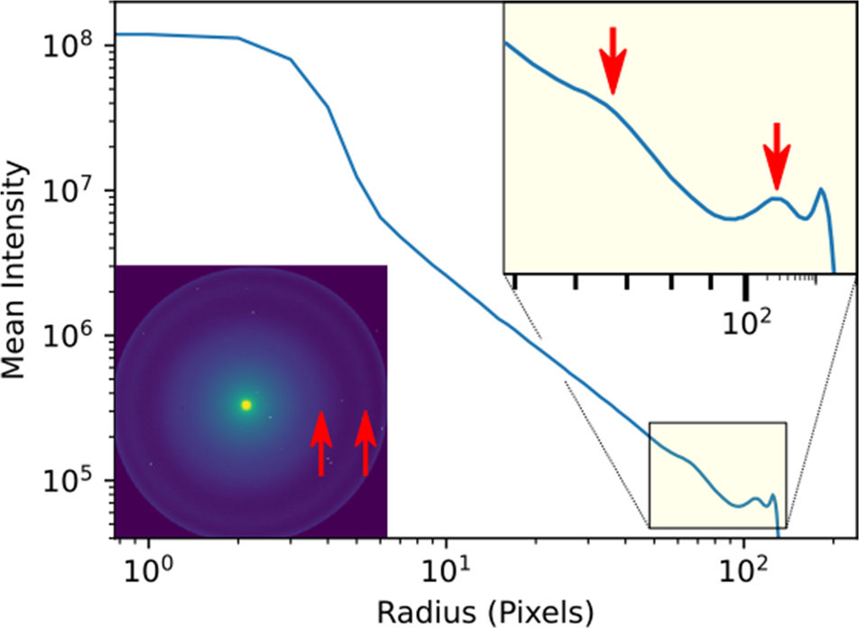
Fig. 2. Radial distribution of scattering intensity from the summed diffraction pattern, shown in the inset, of a 256 × 256 probe position scan of a mouse liver microtome section, calculated using the fpd.fpd_processing.radial_profile function. The pixel spacing was 1.2 nm, the exposure was 4 ms, the semi-convergence angle was 0.436 mrad, the camera length was 180 cm, and the condenser aperture was 10 μm. The arrows mark the location of peaks of intensity.
The scattering angles marked by the peaks in Figure 2 may be used to define one or more virtual apertures. These are simply arrays with values between 0 and 1, corresponding to regions outside and inside the collection angles of interest, respectively, and are applied to the whole dataset by multiplication and then summing the total counts for each mask. Methods for doing this are provided in the synthetic_aperture and synthetic_images functions from the fpd.fpd_processing module, and by the virtual_annular_dark_field method of pixStem's PixelatedSTEM class. The resulting virtual detector images allow the contributions to different scattering angles to be spatially resolved. This approach also works well when using arbitrary, nonannular masks, such as when selecting one or more diffraction spots, where the contrast produced may be used to determine the location and extent of different phases or lattice defects (Gammer et al., Reference Gammer, Ozdol, Liebscher and Minor2015).
With out-of-core processing from compressed HDF5 files, these calculations may take several seconds, depending on the scan size, the computer hardware, and the data chunking. This approach is thus well suited to generating images from known collection angles. While inspection of the diffraction pattern is suitable for identifying the relevant angles in simple cases, it is far more useful to gain live feedback on the changes in spatial contrast from alteration of the virtual detector collection angles. To enable this, the fpd.fpd_processing module also provides the VirtualAnnularImages class. This class maps the radial_profile function, discussed above, across all scan points using the map_image_function function of the same module, and then generates weighted cumulative sums of the radial profiles that may be looked-up at a later point to form the virtual detector image from any given detector geometry. This intermediate dataset is typically ~40–50 times smaller than the 4D one and is currently stored within the class since it can easily fit in memory. For the data in Figure 2, the size is reduced from 8.6 GB to 195 MB. The significantly smaller size of 3D datasets also makes them much more amenable to multivariate analyses such as non-negative matrix factorization (NMF), independent component analysis (ICA), and principal component analysis (PCA).
Once instantiated, virtual images with any possible continuous set of scattering angles may be generated near-instantaneously using the annular_slice method of the class. This calculation time is on the order of milliseconds and, unlike the more flexible synthetic_images approach, the image calculation time does not change with aperture size. A current limitation of this efficiency saving is that center position is taken to be constant across the scan; however, it is not a fundamental one and it could be removed in a future version. As was noted above, in many cases, this limitation is not an issue and, when it is, techniques are available to align the data.
Live feedback on the influence of the virtual detector angles on image contrast may be obtained using the plot method of the VirtualAnnularImages class. Figure 3 shows the two plots created by the plot method (Figs. 3a, 3b) applied to the same data as was used in Figure 2, and images created from the dataset (Figs. 3c–3i). The two vertical features are endoplasmic reticula, each studded with ribosomes. Figure 3a shows a navigation window containing the virtual detector controls, while Figure 3b shows the live image produced by the virtual detector. The navigation window contains a user-supplied navigation image (in this case, a summed diffraction pattern), a measure of the real-space image contrast as a function of the scattering angle, and controls for the starting, ending and center radii for the virtual detector. The detector position and extent are indicated by the red lines in the two plots, and the radii may be changed via the horizontal slider controls with instant updates to the virtual detector image. The real-space image contrast is measured here by the ratio of the variance in the virtual detector image, σ 2, to the image mean, N. For a flat image with Poissonian noise, σ 2 is purely from the noise and is equal to N, so the contrast measure, σ 2/N, would give a value of 1. For nonflat images with the same noise properties, contrast values greater than 1 indicate image signal. Additional noise in the source images will increase the base level and alter the linearity of the contrast parameter of the virtual detector images but it should remain monotonic with image signal. Similar normalized variance measures are routinely applied in fluctuation electron microscopy (Voyles & Muller, Reference Voyles and Muller2002), where the variation is calculated across the azimuth at each radii (scattering angle) in each single image (Hart et al., Reference Hart, Bassiri, Borisenko, Véron, Rauch, Martin, Rowan, Fejer and MacLaren2016). The contrast measure used here is different; it is for the image produced from each single pixel width detector, calculated across all radii near instantaneously using the class itself.

Fig. 3. (a,b) Example of the VirtualAnnularImages class, allowing interactive plotting of virtual annular detector images with instantaneous updates. The sample data are the same as that used for Figure 2, a scan of a mouse liver microtome section showing endoplasmic reticula studded with ribosomes. The partial height colored windows and annotations in (a) have been added to the regular display to mark the locations of the detector geometries used to generate the virtual aperture images in (c–i), from BF to DF. The arrows in (a) show the location of the peaks in the radial distribution presented in Figure 2. The intensity ranges in (c–i) are set to 0.2–99.8% of the range for each panel, and the color bars in each panel show the counts in thousands.
The peaks in the scattering angle dependence plot show which angles produce strong contrast, and are a useful aid in determining the range of angles on which to focus. In the case of the biological sample shown, several peaks are visible, but none of them align with those seen in the radial distribution of Figure 2 (these are also marked by red arrows in Fig. 3a), contrary to what one would expect if the local peaks in diffraction intensity produce images with more contrast. Figures 3c–3i show the virtual images produced at the geometries indicated in the annotations, from BF to ADF, at locations between and at the peaks of maximum contrast. The geometries are also indicated in Figure 3a by the partial height windows matching the order of the images and their colored outlines.
Within the DF, there are three peaks of the contrast parameter, at approximately 46, 79, and 126 pixels (Figs. 3e, 3g, 3i), and these are where the images do indeed show the highest contrast and range of spatial frequencies, allowing the ribosomes to be better resolved, with the best contrast produced from the highest of these scattering angles. To estimate the SNR of each individual image, we apply to them the single image autocorrelation method (Thong et al., Reference Thong, Sim and Phang2001) implemented in the snr_single_image function of the fpd.utils module. This approach exploits the fact that noise is spatially uncorrelated, whereas the signal is correlated, allowing extrapolation of the autocorrelation function to zero image displacement to be used to estimate the noise-free signal power and, thus, the noise power. The optimum extrapolation method depends of the properties of the image and our implementation supports a number of methods. For the data in Figure 3, a linear extrapolation method is adequate and gives values of 20–37 for the first six images (Figs. 3c–3h), and 71 for the highest scattering angle image (Fig. 3i), confirming that it does indeed have a much higher SNR. These SNR values are the power values with the signal magnitudes taken from the changes in the images, as defined in the original method, and thus give measures of the useful contrast.
For the biological sample used here, there is very little Bragg scattering and the ADF contrast changes in the angular range acquired of up to ~15 mrad is likely to be due to incoherent Rutherford scattering from light elements. The rings visible in the diffraction pattern and its radial distribution are equivalent to d-spacings of approximately 0.35 and 0.22 nm and may be indicative of characteristic bond lengths or periodicities in molecules but, as we have shown, do not always yield images of the greatest useful contrast.
The ability to interrogate and reconstruct STEM images showing different contrast from a single scan, post-acquisition, as outlined above, makes the technique of virtual detectors a very powerful one. In addition, unlike the similar hollow cone technique (Krakow & Howland, Reference Krakow and Howland1976; Tsai et al., Reference Tsai, Chang, Lobato, Van Dyck and Chen2016), only one scan is required to generate many types of contrast, making it dose efficient, which is especially useful in beam-sensitive materials.
While we demonstrate the utility of applying virtual detectors with data from a biological sample, the technique is useful in many other applications, where different navigation images may be more appropriate. For example, in polycrystalline samples, the navigation image may be a diffraction pattern from a specific grain, identified from navigating the dataset with the DataBrowser class (see Fig. 1) or a similar method. It is then straightforward to set annular apertures that select specific spots, thereby identifying the extent of the grain of interest and the locations of similar grains. More advanced analysis for out-of-plane and in-plane structural analysis is discussed next, in the sections “Higher-order Laue zone analysis” and “Lattice analysis”, respectively.
Higher-Order Laue Zone Analysis
The intersection of the Ewald sphere with parallel reciprocal planes of a crystal gives rise to concentric circles of reciprocal space where the Bragg condition is met, leading to constructive interference in the diffraction pattern. The central region of the diffraction pattern is formed by the crystal structure perpendicular to the electron beam and is called the zeroth-order Laue zone (ZOLZ). Diffraction spots in HOLZ correspond to intersection of Ewald's sphere with parallel planes of reciprocal lattice points offset along the electron trajectory (formally the electron wavevector in reciprocal space) (Emslie, Reference Emslie1934; Jones et al., Reference Jones, Rackham and Steeds1977). Thus, for an on-axis diffraction pattern, periodicity parallel to the beam results in rings of intensity in the diffraction pattern, as shown in Figures 4a and 4b. The radius, r, of the ring in reciprocal space for the first-order Laue zone is given by:
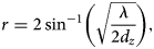 $$r = 2\sin^{-1}\left(\sqrt{{\lambda\over 2 d_z}}\right),$$
where λ is the wavelength of the electron and d z is the lattice period parallel to the electron beam. An equivalent relation was originally derived by Emslie (Reference Emslie1934) in a different form that incorporated the camera length. Similar relations may be derived for higher order Laue zone rings. It has long been recognized that high-angle coherently scattered intensity concentrated in HOLZ rings may affect the contrast in HAADF images (Spence et al., Reference Spence, Zuo and Lynch1989).
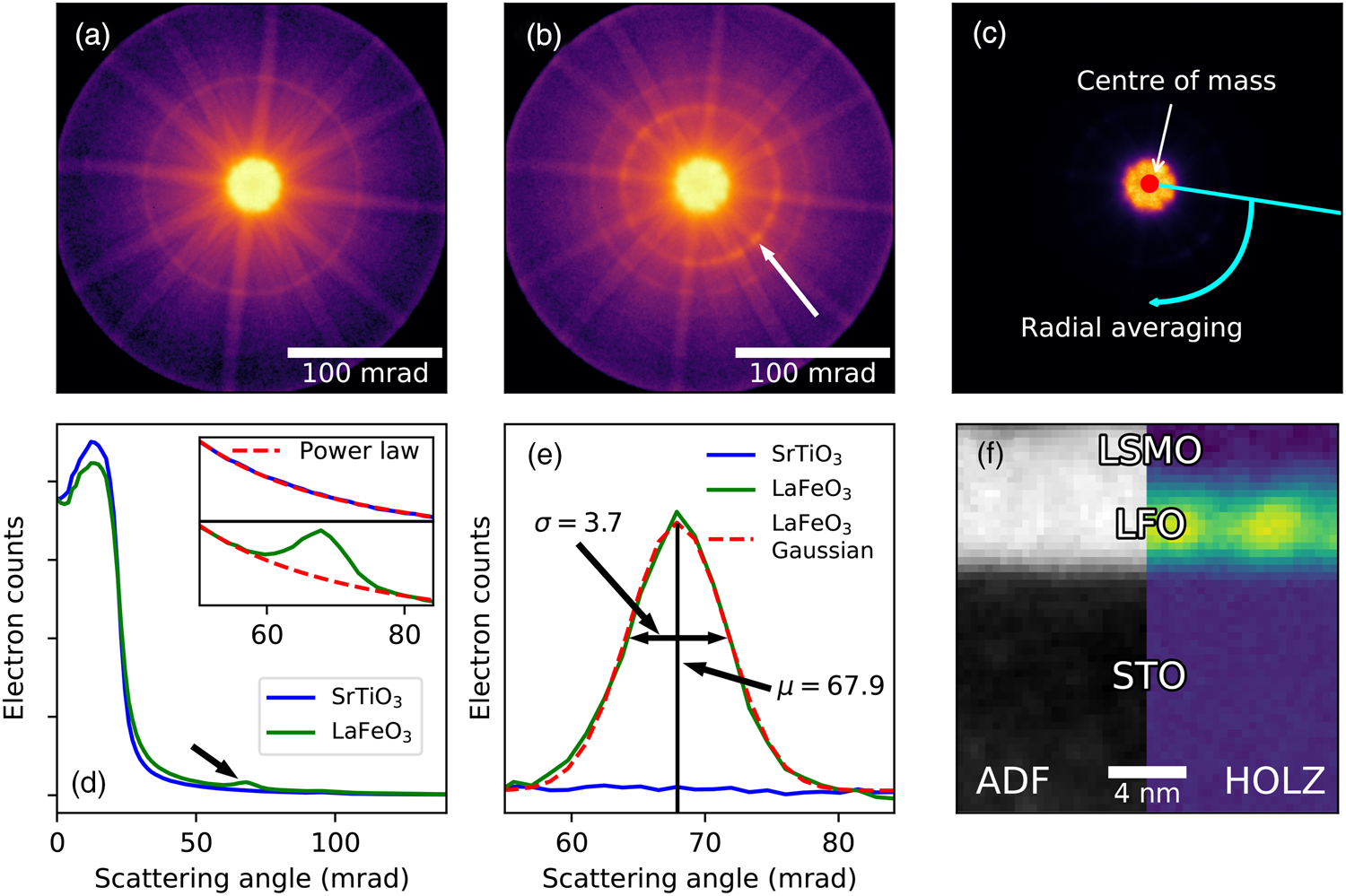
Fig. 4. Processing of HOLZ diffraction rings from a La0.7Sr0.3MnO3 (LSMO) and LaFeO3 (LFO) bilayer film grown on SrTiO3 along the [111] direction. The data were acquired on a probe corrected JEOL ARM200cF, with an acceleration voltage of 200 kV, a convergence semi-angle of 20.4 mrad, a scan step size of 0.37 nm and with a total scan size of 64 × 64 points. STEM diffraction pattern of the (a) STO and (b) LFO, plotted on a logarithmic scale, with the electron beam parallel to the [110] direction. LaFeO3 has an extra inner HOLZ ring due to doubling of the unit cell (arrowed). (c) Schematic of the processing, first using thresholded center of mass to find the center of the pattern, then radial averaging across the azimuth around this point. (d) Radial distribution of (a) and (b). The arrow shows the inner HOLZ peak from (b). The insets to (d) show the region around the HOLZ peak, with a power law fitted to the background. (e) Region around the HOLZ peak, with the power law from (d) subtracted, showing the background is accurately removed, and with a 1D Gaussian profile fitted to the data. Numbers showing the center position and sigma of the Gaussian. (f) Result of the processing for the bilayer system, showing the bright LSMO and LFO regions in the virtual ADF (106–163 mrad) image, and bright LFO region in the HOLZ contrast.
Because of the dependence of the radius on the out-of-plane structure, the presence of HOLZ rings can be used to obtain information about the structure parallel to the electron beam: the smaller the radius of the Laue zone ring, the larger is the distance between atomic planes parallel to the electron beam. This was originally proposed as a method for studying altered periodicity in dislocation core structures (Spence & Koch, Reference Spence and Koch2001) and was later successfully used to determine the periodicity along the beam direction in sodium cobaltite using a simple thin annular detector setup (Huang et al., Reference Huang, Gloter, Chu, Chou, Shu, Liu, Chen and Colliex2010).
Alternative approaches to obtaining such information from crystals are to tilt the sample to high angles, or take multiple specimens containing the same kind of feature cut at different angles and reconstruct using either diffraction tomography (Kolb et al., Reference Kolb, Gorelik, Kübel, Otten and Hubert2007; Mugnaioli et al., Reference Mugnaioli, Gorelik and Kolb2009) or atomic resolution discrete tomography (MacLaren & Richter, Reference MacLaren and Richter2009; Van Aert et al., Reference Van Aert, Batenburg, Rossell, Erni and Van Tendeloo2011; MacLaren et al., Reference MacLaren, Wang, Morris, Craven, Stamps, Schaffer, Ramasse, Miao, Kalantari, Sterianou and Reaney2013). These approaches are not applicable to all samples (e.g., they could not be used on a dislocation core). They are also time-consuming and either use statistical reconstruction from multiple specimens or multiple sample areas (and so assume that the different areas imaged all contain exactly the same structure, just imaged along different directions), or, in the case of the tomographic approach, use a large radiation dose on one area. Moreover, using a thin annular detector is inflexible and needs camera length tuning to get this to work, thus using a fast pixelated detector and detecting and processing the HOLZ data after acquisition is far more flexible for a variety of systems.
One example of a class of materials with structural distortions that cause a change in the size of the unit cell is perovskite oxides, which often exhibit a doubling of the unit cell as a result of octahedral tilting (Glazer, Reference Glazer1972). These distortions are important to characterize, as they can heavily influence functional properties such as ferromagnetism and ferroelectricity. This is especially important in thin film systems, as much of the interesting physics resides in the detailed crystallographic structure of these films. One such example is La0.7Sr0.3MnO3 (LSMO) and LaFeO3 (LFO) bilayer films grown on SrTiO3 (STO) (Hallsteinsen et al., Reference Hallsteinsen, Moreau, Grutter, Nord, Vullum, Gilbert, Bolstad, Grepstad, Holmestad, Selbach, N'Diaye, Kirby, Arenholz and Tybell2016; Nord et al., Reference Nord, Ross, McGrouther, Barthel, Moreau, Hallsteinsen, Tybell and MacLaren2019). While previous work has been performed using ABF or BF imaging in STEM (Aso et al., Reference Aso, Kan, Shimakawa and Kurata2013; Wang et al., Reference Wang, Salzberger, Sigle, Suyolcu and van Aken2016; Kim et al., Reference Kim, Pennycook and Borisevich2017; Nord et al., Reference Nord, Vullum, MacLaren, Tybell and Holmestad2017) to characterize the in-plane oxygen atom movements associated with the octahedral tilting, it is also possible that there are atom movements resulting in a periodicity change along the beam direction. Specifically, while researchers in perovskites and related oxides often talk about octahedral tilting, this rarely happens in isolation and is usually associated with the modulation of cation positions, a feature that is likely to result in a significant diffraction signal.
Figure 4a shows the STEM diffraction pattern of the nondistorted cubic STO substrate imaged along the [110] direction, which has one visible Laue zone ring. The diffraction pattern of the LFO film is shown in Figure 4b, which is noncubic due to structural distortions, and is similar to the LSMO pattern except for having an extra Laue zone ring at lower scattering angles (arrowed). The intensity of this additional ring is proportional to the amount of distortion and can, for example, be used to characterize the strength of the atomic movements as a function of position in thin film structures (Nord et al., Reference Nord, Ross, McGrouther, Barthel, Moreau, Hallsteinsen, Tybell and MacLaren2019) as described below. Additionally, a fine structure can appear in the HOLZ rings and they can split into more than one ring, which may reveal additional subtle details about the structure (Peng & Gjønnes, Reference Peng and Gjønnes1989), and this can be recorded in scanned diffraction datasets at a suitable camera length.
The first step in the processing (Fig. 4c) is finding the center position of the diffraction pattern for each probe position. This is necessary due to the fact that the shift and the tilt of the electron beam is not always perfectly separated in the scanning coils, especially for larger scan areas, and there is no de-scan coil setup in the microscope used in this work, resulting in the diffraction pattern center moving as a function of beam position. As discussed in the section “Virtual detector images”, finding the center position can be nontrival for high convergence angle diffraction patterns like we have here. However, for these samples, the zone-axis remained sufficiently aligned across the scan area for it to be possible to find accurate center positions using a thresholded and masked center of mass procedure. The mask removes the higher scattering angles, so only the region containing the BF disc is included. Then, the thresholding sets all values below the chosen threshold to zero, and all above it to one. The center of mass calculation is done on this masked and thresholded image, resulting in the center position of the diffraction pattern. For more difficult sample data, acquiring a reference dataset in vacuum and performing the same center of mass calculation on this dataset can often provide accurate center positions. Some alternatives techniques for center finding are demonstrated in the section “Direct beam characterization”.
Next, integration is performed along the azimuth for each probe position to generate radial dependencies, as previously discussed in the section “Virtual detector images”, using the aforementioned center positions of the diffraction patterns. This reduces the 4D dataset to 3D: 2 probe dimensions and 1 dimension with intensity as a function of scattering angle, as shown in Figure 4d. By removing one dimension, the data size is reduced by a factor of around the number of pixels on the longest axis of the detector (256, in our case), making it much more manageable and easier to fit into the computer memory. This radial averaging is also useful for data exploration of large datasets like this, due to the much smaller data size, as demonstrated in the section “Virtual detector images”. One complication is distortions caused by the projection system, leading to features which should be round becoming elliptical. When doing the radial averaging, this distortion causes a broadening of the HOLZ peak (Figs. 4d, 4e). However, for sufficiently small distortions, this does not heavily affect the total intensity in the peak. Ideally, this should be corrected for by calculating the diffraction distortions from a reference dataset. However, as the focus of this analysis was the intensity of the peak, no such corrections were performed here.
After the radial distribution has been calculated, the HOLZ ring is reduced to a HOLZ peak shown by the arrow in Figure 4d. To extract the intensity from only the peak, a power law is simultaneously fitted to both the regions before and after the peak. The fits are shown in the insets in Figure 4d, both for the STO which does not have the extra HOLZ peak, and for LFO which has an extra HOLZ peak at lower scattering angles. While a power law is not the optimal function to fit to this type of background over long distances, it works well for extracting the HOLZ peaks over a relatively short range of scattering angles, as shown by the level background of the corrected profiles in Figure 4e.
After background correction, the profiles may be analyzed by simply summing the intensity in the HOLZ peak to give a map of the level of structural distortion, as shown in Figure 4f. Pairing the HOLZ processing with virtual ADF generated from the same radially averaged data, one can see that the extra HOLZ ring is indeed present only in the LFO layer. More information can also be extracted by fitting a 1D Gaussian to the peak, as shown in Figure 4e, giving information about changes in the scattering angle (center position) and variation in scattering angle (standard deviation). Further information on the material aspects from a detailed analysis of this system are published elsewhere (Nord et al., Reference Nord, Ross, McGrouther, Barthel, Moreau, Hallsteinsen, Tybell and MacLaren2019). This type of analysis is best suited for monocrystalline materials, especially epitaxial thin films and heterostructures, or polycrystalline materials with large grains (e.g., domain-structured functional oxides with different orientations of the principal axes of the cell), as the technique requires the crystal to be imaged along a zone axis. While it may be performed at atomic resolution, this is not necessary, and this technique has the advantage that it yields information about the modulation of atomic positions along a column without requiring atomic resolution, as demonstrated in previous analyses of this effect (Borisevich et al., Reference Borisevich, Ovchinnikov, Chang, Oxley, Yu, Seidel, Eliseev, Morozovska, Ramesh, Pennycook and Kalinin2010; Azough et al., Reference Azough, Cernik, Schaffer, Kepaptsoglou, Ramasse, Bigatti, Ali, MacLaren, Barthel, Molinari, Baran, Parker and Freer2016).
Lattice Analysis
Analyzing the crystal structure of materials has been a part of electron microscopy since its inception. A number of techniques in TEM can be used for atomic resolution imaging, most frequently phase contrast TEM (high-resolution TEM, HRTEM) and HAADF STEM. Nevertheless, diffraction-based techniques have been the main method for structure solution or analysis throughout the history of electron microscopy, notwithstanding the advantages of the image-based techniques for giving local crystallographic information, especially where this varies with position such as in thin films, heterostructures, and around defects and precipitates.
Selected area electron diffraction (SAED) can localize the sample region from which data are collected to ~100s nm, much higher than the nanometer or even Ångström length scales that imaging with high-energy electrons can potentially allow. Recently, however, scanned diffraction techniques have been on the increase, especially with the rise of faster electronic detectors (initially CCD/scintillator arrangements, but more recently direct electron detectors). Moreover, the development of SPED (Vincent & Midgley, Reference Vincent and Midgley1994) has allowed collection of spatially resolved diffraction data down to areas of 2 nm or less with very high precision of the reciprocal lattice parameters.
Convergent beam techniques provide the highest spatial resolution by imaging with a probe formed by a large diffraction-limiting aperture, and it is these techniques that have seen the greatest application in materials science in a number of areas, including grain size and orientation determination, molecular structure solutions, and material strain measurement. Strain is a particularly important property that influences the functionality of a wide range of materials, with perhaps the most notable class of materials being semiconductor devices (Cooper et al., Reference Cooper, Denneulin, Bernier, Béché and Rouvière2016; Bashir et al., Reference Bashir, Millar, Gallacher, Paul, Darbal, Stroud, Ballabio, Frigerio, Isella and MacLaren2019).
A number of techniques for strain measurements have been developed (Béché et al., Reference Béché, Rouvière, Barnes and Cooper2013), including dark-field electron holography (DFEH; Hÿtch et al., Reference Hÿtch, Houdellier, Hüe and Snoeck2008; Cooper et al., Reference Cooper, Barnes, Hartmann, Béché and Rouvière2009; Béché et al., Reference Béché, Rouvière, Barnes and Cooper2011), NBED (Béché et al., Reference Béché, Rouvière, Clément and Hartmann2009), SPED (also referred to as nanobeam precession electron diffraction (NPED); Rouvière et al., Reference Rouvière, Béché, Martin, Denneulin and Cooper2013; Midgley & Eggeman, Reference Midgley and Eggeman2015), scanning moiré fringe (SMF) analysis (Su & Zhu, Reference Su and Zhu2010; Naden et al., Reference Naden, O'Shea and MacLaren2018), HRTEM geometrical phase analysis (GPA; Hÿtch et al., Reference Hÿtch, Snoeck and Kilaas1998), and atomic column spacing displacement characterization (Nord et al., Reference Nord, Vullum, MacLaren, Tybell and Holmestad2017). Of these, the best fractional strain precision reported is with SPED at 2 × 10⁻⁴ (Rouvière et al., Reference Rouvière, Béché, Martin, Denneulin and Cooper2013); however, very recent work with patterned probes (Guzzinati et al., Reference Guzzinati, Ghielens, Mahr, Béché, Rosenauer, Calders and Verbeeck2019; Zeltmann et al., Reference Zeltmann, Müller, Bustillo, Savitzky, Hughes, Minor and Ophus2020) have achieved precisions approaching the same value.
Analysis of such 2D lattice images can be performed with a range of packages, including Atomap, optimized for atomic resolution STEM imaging (Nord et al., Reference Nord, Vullum, MacLaren, Tybell and Holmestad2017); CrysTBox for HRTEM, SAED, and convergent beam electron diffraction (CBED) imaging (Klinger, Reference Klinger2017); library-based approaches to crystal phase and orientation identification (Rauch et al., Reference Rauch, Portillo, Nicolopoulos, Bultreys, Rouvimov and Moeck2010); and ones recently developed specifically for 4D-STEM (Savitzky et al., Reference Savitzky, Zeltmann, Barnard, Brown, Henderson and Ginsburg2019; Zeltmann et al., Reference Zeltmann, Müller, Bustillo, Savitzky, Hughes, Minor and Ophus2020). With the rise in the use of fast pixelated detectors in TEM and STEM and the consequent ability to record large data volumes in short times, the need arises for the ability to analyze large numbers of diffraction patterns accurately and automatically. These include images with point-like lattice vertices, created by imaging under Fraunhofer conditions, and in CBED imaging, where the lattice vertices are discs. In the following sections, we report simple processing methodologies that are applicable to general lattice analysis and, in particular, to diffraction patterns produced by techniques, including CTEM, CBED, NBED, and SPED.
To demonstrate our technique, we apply it to a commercially available crystalline MgO substrate imaged in a JEOL ARM200cF TEM operated at 200 kV in SPED mode using a custom (MacLaren et al., Reference MacLaren, Frutos-Myro, McGrouther, McFadzean, Weiss, Cosart, Portillo, Robins, Nicolopoulos, del Busto and Skogeby2020) DigiSTAR precession system from NanoMEGAS. MgO is a widely studied material (Yang et al., Reference Yang, Sha, Wang, Wang and Yang2006) that is used in magnetic tunnel junctions (Parkin et al., Reference Parkin, Kaiser, Panchula, Rice, Hughes, Samant and Yang2004; Zhu & Park, Reference Zhu and Park2006) and is of interest as a room temperature ferromagnetic insulator when strained (Jin et al., Reference Jin, Nori, Lee, Kumar, Wu, Prater, Kim and Narayan2015). Unstrained MgO has an NaCl-type cubic crystal structure which produces a diffraction pattern with a square projection of the reciprocal space lattice when viewed along the 〈100〉 zone axes. The sample was prepared by application of a standard focused ion beam milling procedure (Schaffer et al., Reference Schaffer, Schaffer and Ramasse2012) to a multilayered structure. Electron energy-loss spectroscopy measurements in a probe-corrected STEM mode with convergence and collection semi-angles of 29 and 36 mrad, respectively, using a GIF Gatan QuantumER 965 spectrometer, showed that the ratio of thickness, t, to inelastic mean free path, λ, (t/λ) of the sample was 0.59. Using an MgO density of 3.58 g/cm2 (Egerton, Reference Egerton2011), λ is 137 nm, giving the thickness of our MgO sample as 81 nm, sufficiently thick for there to be significant dynamical effects from multiple elastic scattering.
The standard precession system was modified (MacLaren et al., Reference MacLaren, Frutos-Myro, McGrouther, McFadzean, Weiss, Cosart, Portillo, Robins, Nicolopoulos, del Busto and Skogeby2020) to employ a Medipix3 detector instead of a fast video recording of the fluorescent screen using an external CCD camera. This modification enables improved imaging fidelity and efficiency through the higher detective quantum efficiency and the noise-free readout properties of the direct electron counting detector. Compared to static probes, precessing the electron beam reduces dynamical effects by incoherently averaging over a range of diffraction conditions to give a pseudo-kinematical diffraction pattern, resulting in more uniform diffraction pattern discs (Midgley & Eggeman, Reference Midgley and Eggeman2015).
In the experiment, test data was acquired by imaging MgO along the [100] axis under the following conditions: the beam was precessed at an angle of 1.5° over a 10 ms exposure; the microscope was operated in TEM-L mode, with a spot size of 5; the condenser aperture was 20 μm; the semi-convergence angle was determined from the MgO lattice to be 1.1 mrad; the camera length was 100 cm; and the scan pixel size was 2.2 nm. No exploration of the acquisition parameter space or subsequent optimization of the parameters was performed.
Correcting for the overestimation of the electron counts recorded by the Medipix3 by a factor of 4 due to scattering of 200 kV primary electrons between pixels [see McMullan et al. (Reference McMullan, Cattermole, Chen, Henderson, Llopart, Summerfield, Tlustos and Faruqi2007) for a discussion], we estimate the dose to be approximately 4.5 × 10⁵ e−/nm2. While this is above the low-dose regime needed for most soft or beam-sensitive materials of 102–105 e−/nm2 (Yakovlev & Libera, Reference Yakovlev and Libera2008), there is great scope to reduce the dose through reduction in beam current or, as pointed out by MacLaren et al. (Reference MacLaren, Frutos-Myro, McGrouther, McFadzean, Weiss, Cosart, Portillo, Robins, Nicolopoulos, del Busto and Skogeby2020), by increasing the precession rate in other microscopes that support it.
To enable the SPED datasets to be used more easily, the topspin_app5_to_hdf5 function of the fpd.fpd_io module allows conversion of data originally recorded in the flat native NanoMEGAS TopSpin app5 format to the multidimensional HDF5 format outlined in Part I (Nord et al., Reference Nord, Webster, Paton, McVitie, McGrouther, MacLaren and Paterson2020). Alternatively, the Merlin system (Plackett et al., Reference Plackett, Horswell, Gimenez, Marchal, Omar and Tartoni2013) through which the Medipix3 data are acquired can be programmed to output the data directly to a raw file, while the acquisition is being performed and controlled by the TopSpin software. These datasets can be processed by the fpd and pixStem libraries in a number of ways, including the previously covered virtual detector imaging and Laue zone analyses, and differential phase contrast (DPC) analyses for field mapping, which will be covered in Part III. Indeed, the benefits of SPED brought about by averaging over a range of diffraction conditions has great potential to also improve DPC imaging, as others have very recently also noted and investigated (Mawson et al., Reference Mawson, Nakamura, Petersen, Shibata, Sasakif, Paganin, Morgan and Findlay2020).
Machine learning (ML) approaches to structure analysis have recently been applied to SPED data (Martineau et al., Reference Martineau, Johnstone, van Helvoort, Midgley and Eggeman2019). In contrast, the methodology described below is a “bottom up” one that optimizes precision without knowledge of the context of each image. The processing methodology is modular in design, allowing modification or addition of processing steps, as needed for the specific application and, indeed, could be complemented by ML approaches. Below, we outline the main steps without going into the many options provided to tailor the analysis to the sample data and, subsequently, assess the precision of the technique applied to this dataset.
The general process can be divided into the four main stages of (i) direct beam detection and characterization, (ii) feature extraction and filtering, (iii) lattice parameter estimation, and (iv) synthetic lattice inlier detection and fitting. These steps are outlined in Figures 5–8, which include slightly modified versions of the plots optionally produced by the relevant analysis functions applied to the first diffraction pattern of the MgO SPED scan. Each figure will be discussed in turn; the final results of the analysis are shown in Figure 9 and will be discussed later.
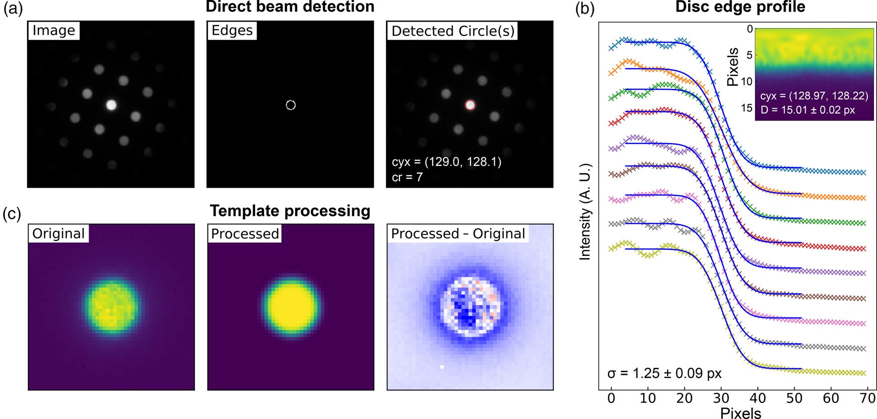
Fig. 5. Lattice analysis stage 1: (a) finding the direct beam, (b) characterization of the disc edge properties, and (c) forming a template using, respectively, the find_circ_centre, disc_edge_properties, and make_ref_im functions from the fpd.fpd_processing module. The lines in (b) are error functions fitted to the data (symbols) taken from the direct beam image converted to polar coordinates, plotted in the inset. The inset also shows the measured diameter of the disc, D, and the optimized center coordinates of the extracted edges. The error in the latter is 0.01 pixels.
Direct Beam Characterization
The first stage in the process is to find the direct beam position and size. Figure 5a shows three images produced in this analysis. The first shows the original image, the second shows the image processed with Canny edge detection, and the third shows the results of a circular Hough transform (Gouillart et al., Reference Gouillart, Nunez-Iglesias and van der Walt2016), where the red circle represents the position and size of the detected disc. This transform generates a 2D Hough space for each radius, with values proportional to the correlation of the edge image and the nominal circle centered at each possible coordinate (the dimensions of the space). The center of the optimized circle is obtained with sub-pixel resolution by fitting 2D Gaussians to each peak in Hough space, or the images may be upscaled. If the lattice vertices are point-like, then the size of the circle represents an effective radius. If the vertices are discs, such as those produced by a convergent beam (or are of any other shape), then a template of the beam image may optionally be formed for use in edge-filtered cross-correlation in order to estimate the position of all vertices in the next steps. As several others have noted, procedures of this type can improve the accuracy of the image registration results by relying more on feature shapes than image intensities (Schaffer et al., Reference Schaffer, Grogger and Kothleitner2004; Krajnak et al., Reference Krajnak, McGrouther, Maneuski, O'Shea and McVitie2016; Pekin et al., Reference Pekin, Gammer, Ciston, Minor and Ophus2017). An important parameter in the analysis is the disc edge profile, and this can be estimated by converting the central beam image to polar coordinates, as shown in the inset in Figure 5b, and then fitting error functions to the edge region, as shown in the main panel. Through this process, the disc diameter and a new center position are also obtained from fitting to the angle dependence of the extracted error curve center positions. Finally, a filtered reference image may be created from the central beam image, using the extracted disc edge width, as shown in Figure 5c. This step further reduces the influence of intensity diffracted from the BF disc, which will not be uniform across all scan points and within all diffraction discs. These nonuniformities in intensity are most easily visible as texture in the rightmost image in Figure 5c, which shows the difference between the real disc and the uniform processed one.
This first stage need only be done once for each dataset, unless the direct beam moves a significant distance during the scan. If this is the case, the direct beam position may be estimated at each scan position using the technique described above, by center of mass as discussed in the section “Higher-order Laue zone analysis”, or by any other means.
Vertex Identification
The second stage in the analysis is to find the position and size of all the potential lattice vertices and then, optionally, to filter these so that only those with inversion symmetry are retained. The results of one way of processing the images to extract potential lattice points are shown in Figure 6. The first step is to perform Laplacian of Gaussian (LoG) blob detection with a supplied radius range, based on the direct beam radius (or effective radius for Fraunhofer imaging conditions). The detected features are shown in Figure 6a by the red circles. If the lattice vertices are point-like, 2D Gaussians may optionally be fitted to extract sub-pixel peak locations. For nonpoint-like or disc-shaped vertices, pixel-resolution edge-filtered cross-correlation (CC) can be used with the template image of the direct beam produced in the first stage. This result is shown in Figure 6b, where the CC peaks, marked by red crosses, indicate the location of maximum correlation, corresponding to the identified vertex locations. By the nature of lattices, cross-correlation can give rise to many false peaks, as is visible in the figure. Therefore, these are filtered by the LoG data which is in general more reliable but which has a higher noise level. Specifically, only those points located within some distance of the LoG vertex coordinates are kept. The peaks retained in this step are marked by black circles. Also at this stage, 2D Gaussian functions can be optionally fitted to the vertices to extract the peak locations with sub-pixel accuracy, as was done here. A comparison of the different analysis levels will be given in the section “Analysis precision”, with reference to Figure 10.
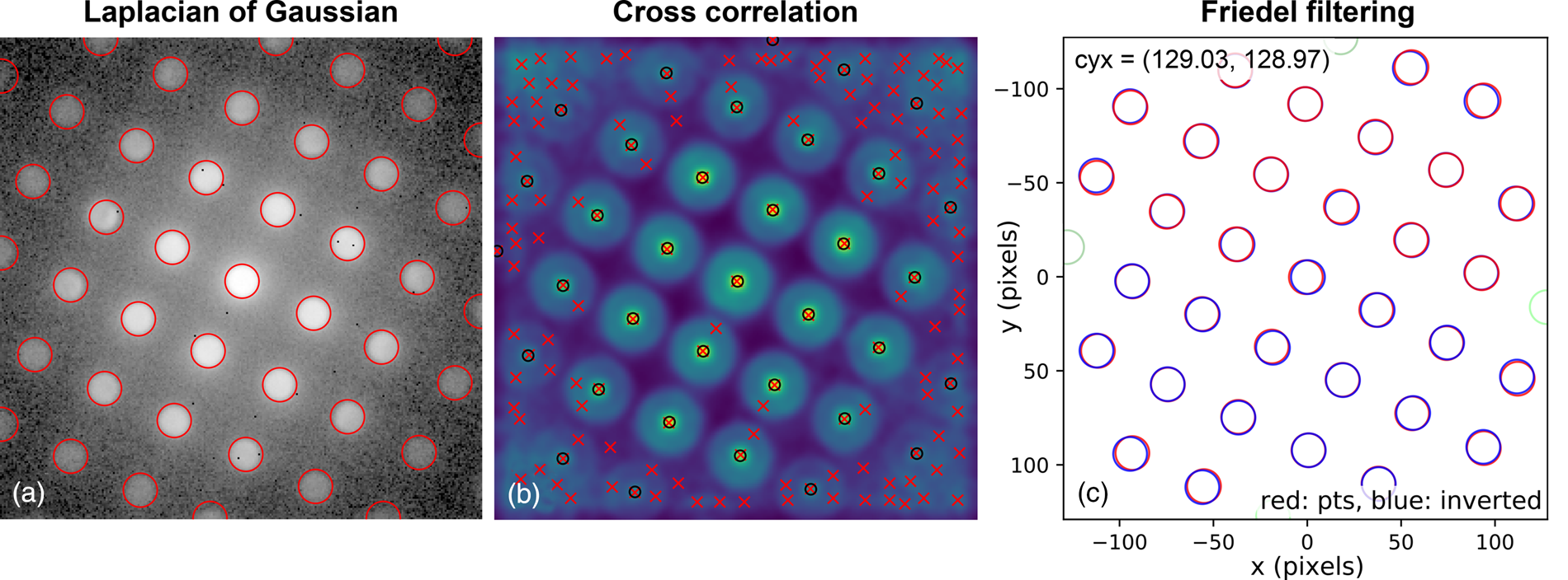
Fig. 6. Lattice analysis stage 2: extracting features and filtering them by inversion symmetry using the blob_log_detect and friedel_filter functions of the fpd.tem_tools module. The red circles in (a) show the blobs detected using LoG applied to a logarithmically scaled image. (b) The results of edge-filtered cross-correlation with a template image, with red crosses indicating peak locations and black circles those filtered for the next step by the LoG data. Green circles in (c) show the discs removed by “Friedel” filtering (see main text for details).
Next, the data are filtered according to Friedel's law (Friedel, Reference Friedel1913), removing points that, within some relative and absolute error, have no equivalent point at the location inverted about the center coordinate. Most of the potential vertices are retained in this example, as shown in Figure 6c, with only those at the edges being removed (shown in green). In this step, the center coordinate may be updated based on the systematic differences in positions of the pairs of diffraction spots, which allows small changes in the position of the direct beam to be accounted for. In this case, the (c y, c x) value was updated to (129.03, 128.97), as shown in the figure annotations.
Lattice Estimation
The previous two stages only extract the positions and sizes of potential lattice vertices and assume nothing of the relationship between these positions, the lattice properties. In the next two stages, the lattice properties are estimated and then optimized from the filtered vertex locations, as shown in Figures 7 and 8, respectively.
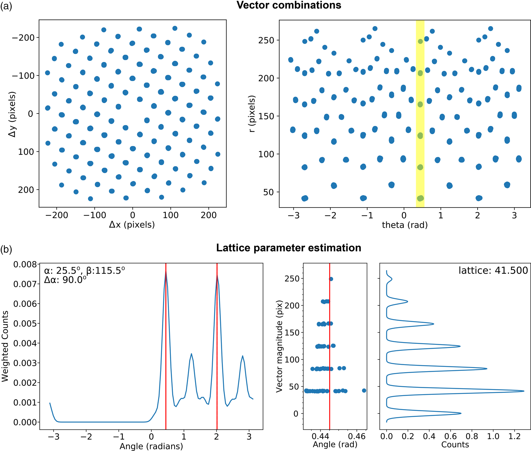
Fig. 7. Lattice analysis stage 3: lattice parameter estimation. (a) Lattice vector combinations in Cartesian (left) and polar (right) coordinates. (b) Lattice angle (left) and magnitude (right) estimates (only one of the two lattice vector magnitude plots is shown).
Fig. 8. Lattice analysis stage 4: lattice parameter extraction. (a) Analysis data (solid symbols) filtered by synthetic lattice (open symbols) inlier detection and (b) the lattice optimized through least squares fitting, where the total error between the two lattices (indicated in the annotations) is minimized. The blue symbol in (b) shows the direct beam location. Outliers would be marked by crosses; however, all data are inliers in this case.
There are many potential ways of estimating lattice parameters and we discuss two of these. First, we use a simple statistical approach, as shown in Figure 7. To improve the statistics, all combinations of lattice vectors are computed (left of Fig. 7a) and converted into polar coordinates (right of Fig. 7a). Next, a histogram is generated from the polar data (left of Fig. 7b), with optional 1/r 2 weighting applied to increase the significance of nearer neighbor data, where r is the Euclidean distance. An expected symmetry of the lattice may be provided at this stage to further improve the analysis. Two peaks are identified from this histogram, marked by the red lines, corresponding to two lattice vector angles. The polar data are then sliced at these angles and a histogram generated (right of Fig. 7b); the equivalent location is marked by a yellow band in the right-hand panel of Figure 7a. The histogram is processed using peak detection or Fourier analysis to extract the lattice magnitudes along these directions, yielding a complete estimate of the lattice parameters.
This simple approach to lattice estimation works best when the sample is on or near a low-order zone axis, and there is a single crystallographic phase within the beam diameter. When multiple lattices are present within a single image, alternative methods to lattice parameter estimation such as clustering and inlier detection may prove to be useful, and can easily be incorporated in the presented processing methodology without modification of the previous or next steps.
The lattice_from_inlier function of the fpd.tem_tools module provides an alternative method of lattice estimation that requires less configuration. This function generates lattices for all combinations of two of each of the first n potential lattice vertex coordinates in distance from the direct beam position, and returns the lattice parameters with the maximum number of inliers to the synthetic lattice, as determined by comparison of the Euclidean distance between matched vertices to a supplied threshold. When multiple lattices have the same number of inliers, one is selected by a user-supplied criterion which, by default, is set to the maximum of the geometrical mean of the lattice parameter magnitudes. This reduces the chances of integer divisions of the lattice parameters being found. As a consequence of this approach, this function typically returns different equivalent lattice parameters across a uniform material. The parameters may be homogenized using the lattice_resolver function described below. Compared to the statistical approach used above with reference to Figure 7, this approach is, in general, more robust against additional spots being present in the image, less robust against there being many missing spots, and produces a slightly less precise but still perfectly usable initial estimate of the lattice.
Lattice Optimization
In the fourth and final step, using an estimate of the lattice magnitudes and angles (generated by any method), a synthetic lattice is created and data inliers to the model are selected. This synthetic lattice and experimental data are shown as solid and open symbols in Figure 8a. Next, the lattice is fitted to the inliers using least squares optimization, resulting in the final lattice shown in Figure 8b. Constraints and bounds on and between lattice parameters can be applied during the fitting process, but none were used for this test data.
The modular design of the lattice analysis makes it easy to assess each processing step, allowing optimization of the analysis parameters, and to customize the processing by inserting additional steps or removing existing ones. Once the processing conditions are established on a test image or images, the analysis may be applied to many images in parallel by passing a user created function to the map_image_function function of the fpd.fpd_processing module.
The four stages outlined above often result in a single unit cell per material. However, as mentioned earlier, it is possible for the particular unit cell returned within a material to change between a number of equivalent unit cells. To condition the data, as an additional step, the lattice parameters extracted can be resolved in specific directions using the lattice_resolver function of the fpd.tem_tools module. This generates a small synthetic lattice using the extracted lattice parameters and then identifies the new lattice vectors by finding those lattice points at angles closest to user specified values. This is especially useful when mapping lattice parameters across epitaxial interfaces between differing materials, where in- and out-of-plane strain may be of particular interest. Potential alternatives that are likely to meet with success include clustering and ML approaches applied to the extracted lattice parameters or parameters derived therefrom. Compared to applying ML approaches to images directly, applying them to the extracted data would vastly reduce the size of the data to be processed (by a factor of several thousands), and also automatically accounts for any de-scan in the measurement as the calculated basis vectors are insensitive to the pattern center position.
MgO Results
Figure 9 shows the results of analyzing the complete MgO SPED dataset, using a reference image for cross-correlation and applying sub-pixel peak fitting. A comparison of the different levels of processing applied the same data is shown in Figure 10 and will be discussed in the section “Analysis precision”.
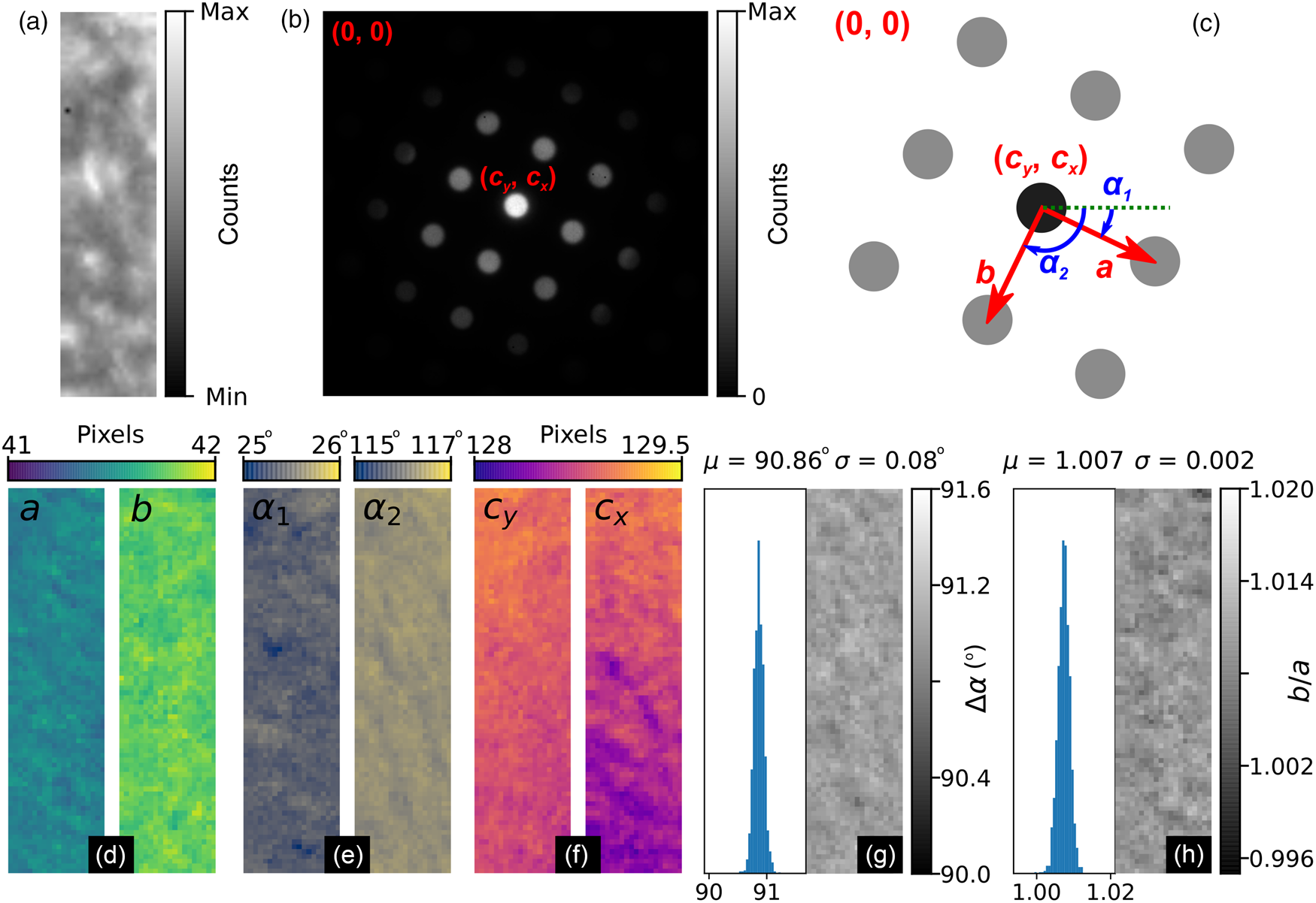
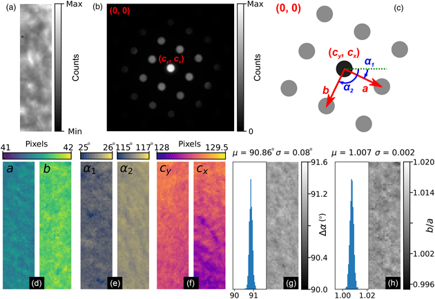
Fig. 9. MgO SPED data analysis results. (a) Real and (b) reciprocal space sum images for an 80 × 20 pixel scan (176 × 44 nm, pixel size: 2.2 nm) using a 256 × 256 pixel Medipix3 detector. The reciprocal space coordinate system is shown in the annotations in (b) and in the schematic in (c). (d–f) Spatially resolved lattice parameters and (g) lattice angle delta and (h) lattice parameter magnitude ratio histograms and maps.
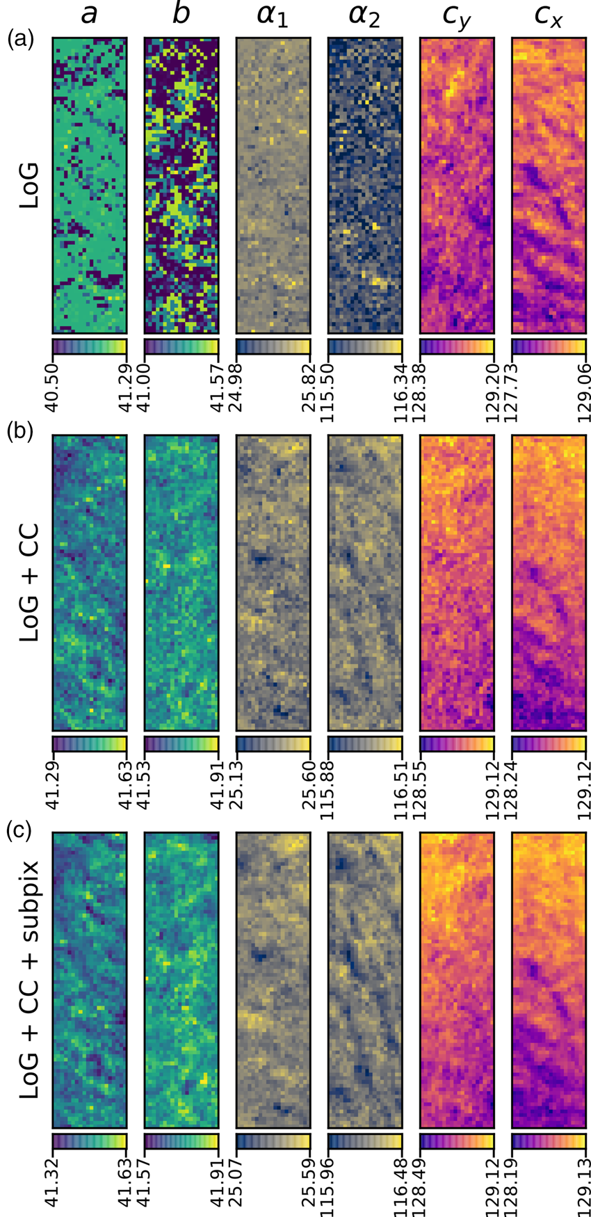
Fig. 10. Comparison of analysis of the MgO SPED data used in Figure 9 with three different approaches (in rows) of generating the diffraction disc centers: (a) Laplacian of Gaussian (LoG), (b) LoG plus cross-correlation (CC), and (c) LoG plus CC plus sub-pixel peak fitting. The units of the data are the same as in Figure 9, pixels and degrees. The color bar ranges are matched to the data range of each panel.
Figures 9a and 9b show the real and reciprocal sum images for the dataset. The reciprocal space coordinate system is defined in Figure 9c. The origin is located at the top left corner, the coordinates of the direct beam are (c y, c x), and the lattice parameters are defined by the magnitudes, a and b, and the angles, α 1 and α 2. The six lattice parameters extracted from the data are shown in Figures 9d–9f, with the angles between lattice vectors, Δα, and the ratio of the lattice magnitudes, b/a, shown in Figures 9g and 9h, respectively.
The mean angle between lattice vectors in the SPED data is 90.86 ± 0.08° (0.09%), and the mean ratio of the lattice vector magnitudes is 1.007 ± 0.002 (0.16%), making for a slightly skewed lattice, and is evidence of strain in our multilayer sample. By comparison, the equivalent lattice vector magnitude ratio for the nanodiffraction MgO data in Figure 1 from a different sample and analyzed by the same method was 1.020 ± 0.006 (0.6%). Although both datasets are influenced by nonuniformities in the MgO, the difference in the variance of the data will reflect to some extent the improvements obtainable by precessing the electron beam.
Care in interpreting the results must be taken in order to rule out the influence of image distortion (Mahr et al., Reference Mahr, Müller-Caspary, Ritz, Simson, Grieb, Schowalter, Krause, Lackmann, Soltau, Wittstock and Rosenauer2019). This may be done in a number of ways, including: recording two or more scans at different sample rotations; recording a reference lattice against which strain parameters (Rouvière & Sarigiannidou, Reference Rouvière and Sarigiannidou2005) can be calculated; or by correcting the lattice vertices by the application of an affine or other transformation to the vertex coordinates from a suitable calibration.
The center coordinates approximately describe planes due to de-scan (as discussed before). However, in samples supporting magnetic or electric fields or exhibiting mean inner potential changes, the beam shifts extracted in these parameters can give useful DPC contrast. Aspects of DPC analysis will be discussed in Part III of this work.
Analysis Precision
Figure 10 shows how the cumulative addition of edge-filtered cross-correlation (Fig. 10b) and sub-pixel peak finding (Fig. 10c) each improve upon the LoG analysis (Fig. 10a). The third row contains the same data as shown in Figures 9d–9f, but the color map scale here is maximized for each panel, with the limits of the ranges shown on each color bar.
The same main features are present in the LoG (first row) data as are in the third row data, but the noise level is much higher and there is a degree of digitization, obscuring the more subtle features. Edge-filtered cross-correlation gives a large improvement, with the spread in parameter values generally reduced and the results are less digitized. This is because the processing technique reduces the influence of intensity variations within the discs and because it is inherently more sensitive to the location of the discs. This will be especially true when the beam is not precessed, such as in CBED or NBED patterns where nonuniformities in the disc intensities can be significantly larger. The improvement over the LoG plus CC results (Fig. 10b) obtained by the addition of peak fitting, shown in Figure 10c, are mainly in the deep sub-pixel range, with a reduction in the random noise level.
To estimate the SNR in these analyses, we applied the same single image autocorrelation power SNR estimation (Thong et al., Reference Thong, Sim and Phang2001) methodology used in the section “Virtual detector images” to the data shown in Figure 10. Here, a second-order polynomial extrapolation of the autocorrelation function was used after de-trending the images with a plane fit, and the signal level was taken from the known zero rather than using the variation in the images. The resulting power SNR values for the a parameters are 64 and 70 dB for the LoG plus CC and LoG plus CC with sub-pixel peak fitting analyses, respectively (the results from the other parameters are similar). The pixelation in the LoG data means we cannot easily extract an accurate SNR estimate for this dataset using this method. However, an estimate of the SNR may be made using the LoG plus CC with sub-pixel peak fitting analysis data as a reference, and this yields a value of 47 dB for the LoG analysis.
The smooth, continuously varying features of our test MgO data means we cannot interpret the level of precision of our approach from the standard deviation of the parameters. However, because we have extracted an estimate of the SNR ratio, we may use this parameter to estimate the fractional precision as  $1/\sqrt {{\rm SNR}}$. The results give a fractional precision of 3.1 × 10⁻⁴ (0.03%) in the LoG plus CC with sub-pixel peak fitting analysis which, with an a parameter of 41.5 pixels, corresponds to a fractional precision of 0.01 pixels of the detector. The fractional precision of the LoG plus CC analysis is about half as good at 6.6 × 10⁻⁴. The theoretical full-width half-maximum (FWHM) spatial resolution of the Airy probe in our measurements, estimated using the airy_fwhm function of the fpd.tem_tools module, is 1.1 nm, which is consistent with direct imaging of the probe. However, at the precession angle used in the experiment (1.5°) and for our sample thickness (81 nm), the center of the probe will describe circles of a diameter of 2.1 nm at the surfaces of the sample and, thus, the actual spatial resolution of the measurement will be poorer than that defined by the static probe. In fact, ignoring the increased weighting of the sampling of the specimen in its vertical center, the FWHM defined resolution of the probe will be given by the diameter of the circle described by the beam. Importantly, if our 2.2 nm scan pixel data were oversampled, our precision estimates may be overly optimistic. As a simple check of this, we repeated the analysis using only every other pixel, giving an interpixel spacing of 4.4 nm, and found the SNR values of the LoG plus CC and LoG pluts CC with sub-pixel peak fitting analyses decreased to 62 and 64 dB, corresponding to precision values of 8.2 × 10⁻⁴ (0.08%) and 6.0 × 10⁻⁴ (0.06%), respectively.
Using the alternative approach of wavelet-based Gaussian noise estimation (Donoho & Johnstone, Reference Donoho and Johnstone1994; Gouillart et al., Reference Gouillart, Nunez-Iglesias and van der Walt2016) yielded very similar fractional precision results to those from the previous analysis with a larger inter-pixel spacing: 7.9 × 10⁻⁴ for the LoG plus CC analysis, and 5.6 × 10⁻⁴ for the LoG plus CC with sub-pixel peak fitting approach, giving credence to the results. Rebinning the data by a factor of 2 along each axis before performing the SNR calculations gives precision values around 4.5 × 10⁻⁴ for both methods. The improvement over using every other pixel is partly due to the increased dose at the same spatial resolution.
Further work is required to determine the optimum acquisition parameters for the accuracy of the analysis. For example, the noise-free readout of the Medipix3 and the relatively low number pixel count of 256 × 256 for a single die (versus several 1,000 s for a typical CCD detector), may mean that better results would be obtained by increasing the camera length so that only the lowest order spots are imaged. Alternatively, different DEDs with higher pixel counts may be used, or more pixels may be added to a Medipix3 detector by tiling the detector chips. The Medipix3 family of detectors are 3-side buttable (Ballabriga et al., Reference Ballabriga, Alozy, Blaj, Campbell, Fiederle, Frojdh, Heijne, Llopart, Pichotka, Procz, Tlustos and Wong2013), and thus may be tiled in 2 × N arrays (Bücker et al., Reference Bücker, Hogan-Lamarre, Mehrabi, Schulz, Bultema, Gevorkov, Brehm, Yefanov, Oberthür, Kassier and Dwayne Miller2020), with larger pixels at the joints which must be accounted for. Furthermore, employment of the through-silicon via feature of the Medipix3 family can allow tiling on all four sides of the sensor in even larger arrays (Tick & Campbell, Reference Tick and Campbell2011; Ponchut et al., Reference Ponchut, Collet, Hervé, Caer, Cerrai, Siron, Dabin and Ribois2015) with minimal dead areas for the readout circuitry.
At the small level of material distortion found here, the fractional precision of the lattice parameters is the same as that of the associated strain parameters. Very recent reports of strain measurements using patterned probes in the literature (Guzzinati et al., Reference Guzzinati, Ghielens, Mahr, Béché, Rosenauer, Calders and Verbeeck2019; Zeltmann et al., Reference Zeltmann, Müller, Bustillo, Savitzky, Hughes, Minor and Ophus2020) approach the best values reported from standard Airy probes in SPED acquisitions (Rouvière et al., Reference Rouvière, Béché, Martin, Denneulin and Cooper2013), but with potential benefits of improved dose efficiency. The fractional precision of 6 × 10⁻⁴ obtained here with a DED is approximately 3× higher than the value from the latter (of ≤ 2 × 10⁻⁴) with a similar spatial resolution, but using exposures 100× smaller and a detector with 64× fewer pixels (256 × 256 DED versus a 2k × 2k CCD). Our results correspond to an approximately 3× higher sub-pixel precision. We cannot compare the beam dose between the two experiments, but we note that the aperture used in our experiment was 2–4× the radius of that used in the referenced work which, taking account of the different exposure times, would give a 25–12.5× reduction in dose in our experiment with a DED if the emission currents were the same. With the noise-free readout of the Medipix3 and the ability to operate in continuous mode, where every individual electron is counted with no gaps, there is great scope for further reducing the sample dose in SPED for use with beam-sensitive materials (MacLaren et al., Reference MacLaren, Frutos-Myro, McGrouther, McFadzean, Weiss, Cosart, Portillo, Robins, Nicolopoulos, del Busto and Skogeby2020).
Method Applicability and Efficiency
We demonstrate the flexibility of our simple lattice analysis method by applying it to the four synthetic lattice images shown in Figure 11. These images were generated by sub-pixel Fourier shifting 2D Gaussian spots of peak intensity 1,024 and include Poissonian noise. The lattices have (a) square, (b) rectangular, (c) hexagonal, and (d) oblique unit cells. These cover four of the five shapes available in 2D space; the remaining one being the rhombic lattice which only differs from the oblique one by having equal lattice vector magnitudes. The extracted parameters are shown in the insets of Figure 11, with the nominal values in parentheses. The agreement between the numbers in this somewhat idealized case is less than around 0.006 pixels and 0.006°, corresponding to an average error of 0.003%, and gives some idea of the accuracy of the algorithm at this electron dose. Ultimately, the final noise and precision achievable will depend on the sample; the imaging conditions, including the dose and beam shape; the characteristics of the detector and its number of pixels; and the parameters used in the analysis.
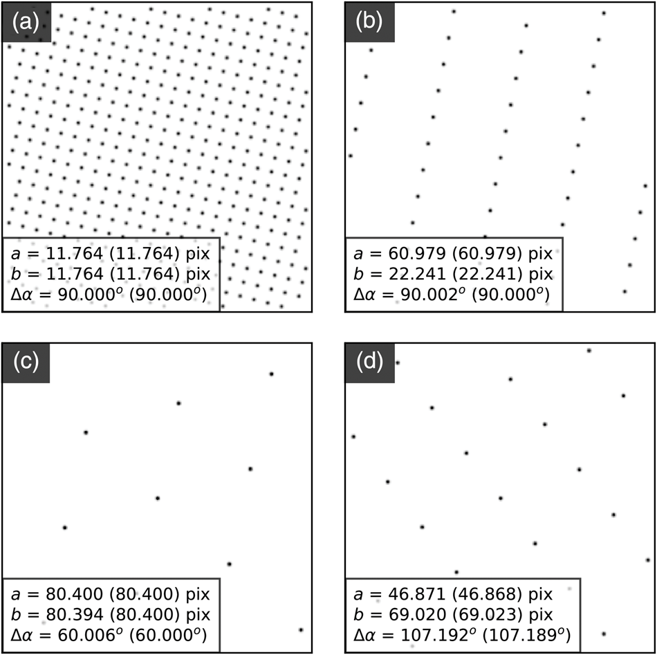
Fig. 11. Four different synthetic lattices and, in the inset text, the results of their analysis using identical processing parameters. The nominal values are given in parentheses. All spots were of equal counts before application of Poissonian noise.
Despite the widely varying lattice size, aspect ratios, and symmetries, the same analysis parameters were used to extract the lattice properties across all four datasets in Figure 11 at the same time, demonstrating the ability of the approach to characterize multiple materials in a dataset without prior knowledge or constraints on what they are. An example of the application of this feature is given in the section “Data visualization”, where multiple phases were identified from experimental nanobeam diffraction data without modification of the analysis parameters. However, many analysis parameters may be specified to improve the parameter extraction in real data, including the ability to apply arbitrary constraints on the lattice parameters, potentially allowing more accurate data extraction for known materials by removal of unneeded degrees of freedom.
In data with only Poissonian noise, the relative error of the extracted parameters,  $\sigma _v / \bar {v}$, will generally follow:
 $${\sigma_v\over \bar{v}} = {m\over \sqrt{N}}\comma\; $$
where N is the total counts and m is a constant that varies with the analysis method used and the properties of the source data, such as the intensity distribution within each lattice spot or disc. To estimate m in our approach, we calculated the ratio of the standard deviation to the mean of the smaller lattice parameter, a of the synthetic lattice in Figure 11d across approximately 1,000 images with different Poisson noise, as a function of the total dose, N. This data is plotted as red circles in Figure 12 for the LoG plus sub-pixel peak fitting analysis of each image, along with a fit to the data of the above equation (black line). The value of m is 0.018 across the dose range investigated of 273 to 140k counts (see inset for examples of a typical lattice vertex as a function of dose). By comparison, the same accuracy data for an analysis by fitting a 2D Gaussian function to each of just two of the lattice vertices is shown as blue crosses and has a much higher m value of 0.178. The equivalent m value obtained by reducing N to the counts in 2 of the 21 vertices is 0.039, around twice that found by using all vertices, showing the benefit of using all available counts.
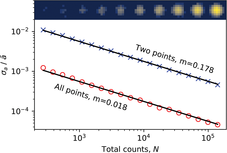
Fig. 12. Relative error of the smaller lattice parameter magnitude, a, of the lattice in Figure 11d as a function of dose. The data were analyzed using LoG feature detection plus sub-pixel peak fitting, using the full lattice (all points) and the central spot and one other point (two points). The inset shows example images of every other spot as a function of dose, on a logarithmic intensity scale.
This approach of fitting to the complete lattice makes use of every vertex and all available signal, optimizing the accuracy for a given dose, as well as extracting more information in the form of the other lattice parameters. The imperfections in real data will mean that the precision of our approach applied to such data will most likely be significantly lower than the characteristic values reported in Figure 12, and will be dependent on the properties of the sample and the detector, but the benefits of our approach will remain; specifically, that by using all vertices, the signal is used optimally and the effect of systematic variations in vertex properties, such as background variations, will be reduced.
Regardless of the source of the data, once the shape of a lattice has been characterized, it is then possible to extract additional information. For diffraction data, this includes strain mapping, the number and spatial extent of different phases or grains (see Fig. 1), and the spot intensities for structure factor characterization (Midgley & Eggeman, Reference Midgley and Eggeman2015) and structure determination (Mugnaioli et al., Reference Mugnaioli, Gorelik and Kolb2009; Clabbers et al., Reference Clabbers, van Genderen, Wan, Wiegers, Gruene and Abrahams2017; Bücker et al., Reference Bücker, Hogan-Lamarre, Mehrabi, Schulz, Bultema, Gevorkov, Brehm, Yefanov, Oberthür, Kassier and Dwayne Miller2020), and for the analysis of noncentrosymmetric crystals. Intensity mapping may be done by generating a synthetic aperture based on the extracted lattice parameters and then applying it to the data, as discussed in the section “Virtual detector images”, or, for point-like spots, fitting a 2D Gaussian to the peak regions using the functions provided in the fpd.utils module, which are also used in the sub-pixel peak finding described above, yielding details of the peak properties.
Summary
In this work, we discussed the key issues around post-acquisition analysis of data from fast pixelated detectors and presented software libraries to allow efficient data processing and visualization. We provided examples of their use across a number of applications in the area of structural characterization, including the techniques of virtual detector imaging for BF and DF imaging, HOLZ analysis for extraction of structural information along the path of the beam, and nanobeam and scanning precession electron diffraction for lattice parameter determination and strain analysis.
While the data analysis algorithms and libraries presented are applicable to data from any detector, the examples provided show that highly dose efficient active pixel direct electron detectors such as the Medipix3 perform excellently as universal STEM detectors, despite their relatively low pixel counts. Indeed, we have demonstrated a nanoscale lattice parameter mapping in an SPED mode with a fractional precision ≤6 × 10⁻⁴, approaching the best values reported in the literature. Furthermore, in addition to being of use as a regular STEM detector, with every electron being recorded noise-free, there is excellent prospects for the application of the detector to the characterization of beam-sensitive materials.
The software packages presented are hosted in public repositories (fpd devs, 2015; pixStem devs, 2015; fpd demos devs, 2018), are under active development and contain many more features than are covered in this part or in Part 1 (Nord et al., Reference Nord, Webster, Paton, McVitie, McGrouther, MacLaren and Paterson2020) of this work. These packages are provided under an open source licence, allowing full transparency of the algorithms implemented and for them to be continually improved upon by the community.
Part III of this work will cover post-acquisition processing and visualization of data from fast pixelated detectors for differential phase contrast imaging.
Acknowledgements and author contributions
G.W.P. and M.N. were the principal authors of the fpd and pixStem libraries reported herein (details of all contributions are documented in the repositories) and have made all of these available under open source licence GPLv3 for the benefit of the community. R.W.H.W., A.R., and K.A.P. have also made contributions to the source codes in these libraries. G.W.P and M.N. have led the data acquisition and analysis, and the drafting of this manuscript. The performance of this work was mainly supported by Engineering and Physical Sciences Research Council (EPSRC) of the UK via the project “Fast Pixel Detectors: a paradigm shift in STEM imaging” (Grant No. EP/M009963/1). G.W.P. received additional support from the EPSRC under Grant No. EP/M024423/1. M.N. received additional support for this work from the European Union's Horizon 2020 research and innovation programme under the Marie Skłodowska-Curie grant agreement No. 838001.
R.W.H.W., A.R., K.A.P., T.A.M., D.McG., and I.M. have all contributed either through acquisition and analysis of data or through participation in the revision of the manuscript. The studentships of R.W.H.W. and T.A.M. were supported by the EPSRC Doctoral Training Partnership Grant No. EP/N509668/1. I.M. and D.McG. were supported by EPSRC Grant No. EP/M009963/1. The studentship of K.A.P. was funded entirely by the UK Science and Technology Facilities Council (STFC) Industrial CASE studentship “Next2 TEM Detection” (No. ST/P002471/1) with Quantum Detectors Ltd. as the industrial partner. As an inventor of intellectual property related to the MERLIN detector hardware, D.McG. is a beneficiary of the license agreement between the University of Glasgow and Quantum Detectors Ltd.
We thank Diamond Quantum Detectors Ltd. for Medipix3 detector support; Dr. Bruno Humbel from Okinawa Institute of Science and Technology; and Dr. Caroline Kizilyaprak from the University of Lausanne for providing the liver sample; Dr. Ingrid Hallsteinsen and Prof. Thomas Tybell from the Norwegian University of Science and Technology (NTNU) for providing the La0.7Sr0.3MnO3/LaFeO3/SrTiO3 sample shown in Figure 4; and NanoMEGAS for the loan of the DigiSTAR precession system and TopSpin acquisition software. The development of the integration of TopSpin with the Merlin readout of the Medipix3 camera has been performed with the aid of financial assistance from the EPSRC under Grant No. EP/R511705/1 and through direct collaboration between NanoMEGAS and Quantum Detectors Ltd.
Data and Software Availability
The complete source data and scripts to analyze the data and produce the results presented here are publicly available at http://dx.doi.org/10.5281/zenodo.3903517 (Paterson et al., Reference Paterson, Webster, Ross, Paton, Macgregor, McGrouther, MacLaren and Nord2020). The software presented in this work is available in public Git repositories (fpd devs, 2015; pixStem devs, 2015; fpd demos devs, 2018).


 Open access