

DISCUSSION POINTS
• Flexible solar cells based on inorganic materials can be divided into three main categories: thin film, low-dimensional materials, and bulk material. Various thin film materials have been studied to achieve flexible cells using both the substrate and superstrate configurations including a-Si, copper indium gallium selenide (CIGS), cadmium telluride (CdTe), III–V, and perovskite. Future progress is bright for a-Si, CIGS, and CdTe thin film-based solar cells on a wide range of flexible substrates. While III–V materials achieve the highest efficiencies over all other materials, their high cost inhibits their mass commercialization and limits their production to niche markets (space and defense). A low-dimensional material-based solar cells including quantum dots (QDs) and nanowires have exhibited low efficiencies so far with the added concern of cell-to-cell variability. The corrugation-based flexible solar cells are promising due to their capability to transform rigid and large-scale commercial Si cells into their ultra-flexible and rollable versions with high efficiencies.
• Stretchable solar cells, which are more recent than their flexible counterpart and not commercialized yet, can be divided into three main categories: ultra-thin microcells interconnected with downward buckled interconnects, microwires embedded in an elastomer, and corrugated bulk solar cell based on the interdigitated back contact technology.
• Flexible and stretchable cells need to be encapsulated in a low-cost polymer that exhibits excellent transparency, low water vapor transmission rate, good stability, and UV resistance.
Introduction
The fluctuating cost of energy, due to multiple reasons including geo-political controls, national or international economic disputes, and the fact that available energy resources are limited, is the main motivation to switch to a clean energy world. Photovoltaic energy is one among several clean energy technologies to achieve this transition with attractive prospects. In fact, the supply provided by solar energy is pollution-free and unlimited; in addition, the world receives a daily amount of sunlight that is enough to cover the yearly world energy demand which confirms the merits of this resource.Reference Ruan, Ding and Wang1,Reference Archer and Green2 As a result, solar cells are currently being widely deployed as continually their costs are reduced, while their efficiencies are improved over the years. Flexible and stretchable solar cells in specific have gained increased attention in recent years due to their capability to widen the range of potential solar energy applications, such as integrated photovoltaics, in addition to lowering production costs.Reference Hwang3,Reference Chen4 In fact, until now, Si-based solar devices dominate the photovoltaic market, while the silicon substrates account for the major portion of the production cost. In order to minimize the production cost is through the development of the solar cells on the inexpensive flexible substrates. This would also diminish the transportation and installation costs and enable roll-to-roll (R2R) manufacturing, thus minimizing the complete system price. Moreover, several niche applications require the use of flexible electronics, and thus, in order to make them self-powered, the integration of flexible solar cells would be needed. Portable electronics, wearable electronics, and vehicle-integrated devices are a few examples where integrated solar cells should be flexible, whereas using rigid cells would affect the shape of the vehicle or the drone for instance and therefore affect its aerodynamics.
In terms of materials, silicon has been comprehensively studied since the 1950s. While monocrystalline and polycrystalline silicon-based cells provide enhanced efficiency, amorphous silicon-based cells – which were developed since the 1970s – exhibit lighter weight and thinner thickness that are desirable characteristics for the development of flexible cells.Reference Carlson and Wronski5,Reference Fu, Xu, Li, Sun and Peng6 In recent years, a variety of materials have been investigated for improving the performance of flexible solar cells at each component of the device, such as flexible electrodes based on ITO conductive films and flexible substrates.Reference Zhang, Öberg, Du, Johansson and Johansson7,Reference Cao, Yang, Jiang, Lin and Li8 The main challenges remain in the development of flexible solar cells which maintain an excellent mechanical resilience, stability, lightweight, in addition to a high efficiency comparable to their rigid counterpart and low cost. The first stretchable solar cells were reported in late 2011, coinciding with the advances in wearable and foldable electronics, which are potential applications. As a result, significant progress has been achieved in developing and manufacturing different kinds of flexible and stretchable solar cells. This review will focus on the latest advances in flexible and stretchable solar cells based on inorganic materials.
Flexible solar cells
Thin films
Amorphous silicon thin film
Due to the capability to deposit hydrogenated amorphous silicon (a-Si:H) on large areas with high yield, a-Si:H thin films have been widely employed in both rigid and flexible electronic devices with large areas (e.g., on a 5.7 m glass substrate).Reference Ito, Kato, Komoto, Kichimi and Kurokawa9,Reference Wipliez, Löffler, Heijna, Slooff-Hoek, de Keijzer, Bosman, Soppe, Schoonderbeek, Stute, Rubingh, Furthner and Kruijt10 This was achievable thanks to the capability of the plasma-enhanced chemical vapor deposition (PECVD) system – which is dedicated for the deposition the a-Si thin films – to scale up the processes and to enable moving the large substrates after long deposition times sequentially without the need for a “time off.”
The growth of a-Si on a wide range of flexible substrates has been possible, including metals and plastics that can endure high temperature processes (e.g., polyimide), as well as plastics which require low temperature processes [e.g. polyethylene terephthalate (PET) and polyethylene naphthalate (PEN)]. Paper substrates based on cellulose have also been used in the development of a-Si-based solar cells; however, they are limited to low power niche applications with limited efficiency (~6%).Reference Smeets, Wilken, Bittkau, Aguas, Pereira, Fortunato, Martins and Smirnov11 Moreover, two different configurations for solar cells were successfully reported, including the substrate configuration based on the n–i–p structure that is achieved on opaque substrates, such as metals and high temperature enduring materials, and the superstrate configuration based on the p–i–n structure which requires a transparent substrate, such as flexible glass (Fig. 1).

Figure 1. Superstrate (left) and substrate (right) configurations for a-Si thin film-based solar cells, and the different layers are deposited in sequence on the substrate.
Neverthesless, the transfer process of the active layers of the solar cell can be achieved regardless of the type of the substrate. In the following, the different types of substrates used in the development of a-Si-based solar cells are reviewed, where Table 1 reports some of the promising efficiencies achieved on the different flexible substrates.
Table 1. Efficiencies of a-Si:H solar cells on different flexible substrates.

In terms of commercial status of flexible solar cells, it should be noted that a-Si-based solar cells have been the most fruitful so far. Uni-Solar was able to manufacture multi-junction solar cells on six lines of 2.5 km stainless steel foil in one run and with a high efficiency. As a result, several companies were inspired by the R2R technology achieved at Uni-Solar and introduced it into their manufacturing processes.Reference Jeyakumar, Verma, Díaz, Guerrero-Lemus, Cañizo, Tabarés, Rey-Stolle, Grane, Korte, Tucci, Rath, Singh, Todorov, Gunawan, Rubio, Plaza, Diéguez, Hoffmann, Christiansenm and Cirlinopq12 PowerFilm and Fuji electric commercialized smaller solar cells (<25 MW) using Kapton as the flexible substrate, while Dutch and Swiss companies (Akzo-Nobel Solar and Flexcell, respectively) developed solar cell products on polyester foils; however, they were not commercialized mainly due to economic reasons. In terms of available equipment for the R2R development of flexible solar cells, few possibilities exist, as most of the companies have customized their own tool. Nevertheless, Applied Materials based in the USA provides R2R PECVD tools, while Meyer Burger provides encapsulation tools.Reference Morrison, Morrison, Stolley, Hermanns, Reus, Deppisch, Bolandi, Melnik, Singh and Griffith Cruz13
Metal foil substrate. Metal foils based on aluminum and stainless steel have been reported as successful substrates for a-Si-based photovoltaic cells, especially the latter which has been adopted as a commercial substrate by Uni-Solar.Reference Wipliez, Löffler, Heijna, Slooff-Hoek, de Keijzer, Bosman, Soppe, Schoonderbeek, Stute, Rubingh, Furthner and Kruijt10 Metal foil substrates enable the deposition of the active layers of the solar cell at the optimized high temperatures which are needed to achieve high efficiencies, in addition to being low cost and ultra-flexible with the possibility of the roll-to-roll production. However, the main challenge that arises when using opaque metal foil-based substrates is that the monolithic integration becomes more difficult to achieve. Nevertheless, multiple types of solar cells have been reported by direct deposition on the substrate without the need for transfer, including single-junction a-Si, double-junction a-Si/a-SiGe, and triple-junction a-Si/a-SiGe/a-SiGe.Reference Soppe, Dörenkämper, Notta, Pex, Schipper and Wilde14–Reference Dong, Song, Yoon, Jung, Kim, Kim and Lee18 The PECVD tool was used to grow these layers.
It should be noted that the stainless steel substrate requires planarization to get rid of features that protrude beyond the surface. One potential solution is to use a UV lacquer coating which allows the monolithic integration of devices in series [0], in addition to enabling the nanoimprint lithography with improved light scattering.Reference Soppe, Dörenkämper, Notta, Pex, Schipper and Wilde14 In fact, nanoimprint lithography and anodization have been widely employed to texture the metal foil substrates. For instance, the anodization of Ti foil resulted in 3D nanodent patterns [Fig. 2(a)], which enhanced light scattering in an a-Si-based solar cell such that a power conversion efficiency of 8.05% was achieved.Reference Lin, Xu, Yu, Lu, Min Yin, Tavakoli, Chen, Yuying Hao, Fan, Cui and Li15 The results show that the efficiency degraded by only 3.4% when bent at a 120° for up to 10,000 cycles. Moreover, Al foil has been textured using anodization to make plasmonic nanopatterns,Reference Tsao, Søndergaard, Kristensen, Rizzoli, Pedersen and Pedersen16,Reference Xiao, Wang, Huang, Lu, Lin, Fan, Chenb, Jeongd, Zhua and Li17 while R2R NiFe foil has been anodized and used as a substrate for a-Si-based solar cells for application in water splitting.Reference Dong, Song, Yoon, Jung, Kim, Kim and Lee18

Figure 2. (a) A flexible a-Si solar cell on a patterned Ti foil covered with the polydimethylsiloxane (PDMS) nanopillar membrane and its performance versus bending cycles. Reprinted with permission from Ref. Reference Lin, Xu, Yu, Lu, Min Yin, Tavakoli, Chen, Yuying Hao, Fan, Cui and Li15 .. (b) Electrical and mechanical performance of the a-Si solar cells on nano-textured polymer with nano-holes (NH) and with the addition of the antireflective coating on the nano-holes (NHAR). Reprinted with permission from Ref. Reference Zhang, Song, Wang, Yin, Zhu, Tian, Wang, Chen, Fan, Lu and Li19 of the a-Si solar cells on nano-textured polymer with nano-holes (NH) and with the addition of the antireflective coating on the nano-holes (NHAR). Reprinted with permission from Ref. Reference Zhang, Song, Wang, Yin, Zhu, Tian, Wang, Chen, Fan, Lu and Li19. (c) a-Si solar cells on a 40-μm-thin silicon substrate. The plots on the right show the minority carrier lifetime characteristics of the a-Si film prepared by sputtering at different DC plasma power. Reprinted with permission from Ref. Reference Balagi, Dauksher, Bowden and Augusto20.
Polymeric/plastic substrate. The fabrication of a-Si solar cells on polymeric/plastic substrates can be either achieved on substrates which can endure high temperatures but are costly or on inexpensive and flexible substrates that are sensitive to high temperatures. The two categories differ in terms of the corresponding glass transition temperature. First, the substrates which can endure high temperatures enable the direct growth of the thin films on the substrate at their optimum temperatures (~200 °C), because they show a higher transition temperature than that of the film. The films that can be grown in this case are not limited to the a-Si layer and also other layers including metal electrodes. Polyimide has widely been employed as a high temperature-resistant substrate; however, its high cost does not make it a commercially viable solution. Nevertheless, several companies have commercialized such solar cells including Powerfilm and Fuji Electric, which reported a 12% efficiency in a double-junction a-Si solar cell based on the substrate configuration and using a “series connection via apertures formed on the thin film” structure for integrating multiple cells in series by the R2R process.
On the other hand, the temperature-sensitive substrates have a lower transition temperature than the films to be deposited and thus limit the thin film growth conditions. Nevertheless, these substrates have gained a lot of interest because of low cost and ability to simplify the monolithic integration of the cells for commercialization purposes where the cells can be fabricated using the superstrate configuration. However, it should be noted that this category of substrates makes the direct growth of the active layers more challenging, including the a-Si and the patterned front contacts or the patterned back reflector. This is because these layers generally require processing temperatures that are above the transition temperature of the low cost substrate. In addition, other processes can be difficult to achieve, such as laser scribing and annealing, which increase the temperature locally and globally, respectively, and thus can be problematic. Therefore, to overcome these issues, two main approaches are followed, either the growth and fabrication of the complete solar cell at required high temperatures on a sacrificial substrate, followed by the release and transfer of the active layers onto the flexible substrate, or the development of the complete solar cell at temperatures below the glass transition temperature of the flexible substrate (generally <150 °C). For the approach that requires transfer of the active layers, the fabrication is usually done on the sacrificial substrate followed by attaching the active layers onto the permanent flexible substrate and finally removing the sacrificial substrate. Demonstrated lift-off techniques for a-Si:H PV cells employ glass as a sacrificial substrate,Reference Wang, Shi, Zhao, Diao and Wang21 a colloidal transfer-printing technique,Reference Yang, Sheng, Wu, Chen, Zhou, Zhou, He, Gao and Ye22 or water-assisted transfer printing.Reference Lee, Kim and Zheng23 The latter method showed an efficiency of ~7% for an a-Si:H single junction. For instance, the Helianthos concept of lift-off uses a sacrificial metal foil substrate on which the active layers of the solar cells are completely fabricated, then the device is attached on a permanent flexible substrate while the metal foil would be etched using a metal etchant. Next, the device would be encapsulated using a polymer with a low water vapor transmission rate.Reference Wang, Shi, Zhao, Diao and Wang21
On the other hand, the approach which requires low temperature fabrication processes can be divided into two main areas: substrate or superstrate cells where the back or front surfaces are textured, respectively. In general, the texturing process is conducted at high temperatures (>300 °C) where the silver is naturally textured via deposition using the substrate configuration, while in the superstrate configuration, the transparent conductive oxide (TCO) is naturally textured via deposition at temperatures >400 °C.
In order to eliminate high temperature processes, one way is to use a substrate that is pre-textured via a specific process, such as lithography, hot embossing, or holographic gratings. It is worth mentioning that some of these methods can also be applied on substrates that can endure high temperatures. A group of researchers at ecole polytechnique Federale de Lausanne (EPFL) reported a world record efficiency in a-Si-based solar cells on a PEN low cost and flexible substrate via lithography [Fig. 2(b)]. In addition, an efficiency of 8.17% has been achieved recently on the nanotextured polymer substrate using the sol–gel-based nanoimprinting method where an antireflective coating deposited on the nanoholes resulted in further enhancement.Reference Zhang, Song, Wang, Yin, Zhu, Tian, Wang, Chen, Fan, Lu and Li19 The device also showed a degradation of around 17% in the efficiency when bent up to 180°, while the degradation is neglibigle after even 100,000 bending cycles [Fig. 2(b)].
Another way to avoid high temperature processes is to texture the TCO after growth using a wet etchant. For instance, ZnO-based TCO can be patterned into inverted pyramidal shapes using a solution based on HCl.Reference Wilken, Finger and Smirnov24 It should be noted that this technique is also applicable on substrates which can endure high temperatures. In this case, the ZnO is magnetron sputtered at room temperature, but the actual temperature on the substrate can reach up to 100 °C due to the bombardment during the deposition process. Using a substrate configuration, the ZnO would be magnetron sputtered, then etched using HCl to texture it, followed by the growth of Ag- and Al-doped ZnO and finally growth of the active n–i–p layers including the front contacts. In a superstrate configuration, the development of the solar cell would be based on the initial growth of the Al-doped ZnO followed by etching using HCl to texture it, and finally, the active p–i–n layers are deposited with the back contacts. Even though this sounds simple, the thickness of the TCO layer might create problems where a thick layer induces compressive stress that causes the foil to curl, resulting in cracks in the active layers of the device. Therefore, it is important to ensure that all sides of the substrate are covered with the same thickness of TCO while etching one side to texture it. Additional processes are also critical to avoid exposing the ZnO to humidity as is it moisture-sensitive, and this includes the deposition of a barrier layer between the ZnO and the polymer,Reference Yang, Sheng, Wu, Chen, Zhou, Zhou, He, Gao and Ye22 or to treat the ZnO with hydrogen or argon.Reference Jeong, Kim, Park, Kim and Choi25,Reference Águas, Mateus, Vicente, Gaspar, Mendes, Schmidt, Pereira, Fortunato and Martins26
Thin glass substrate. An ultra-thin layer of glass exhibits flexural rigidity, in addition to a unique encapsulation characteristic, low water vapor transmission rate, high temperature resistance, high transparency, and light weight that makes it advantageous over metal foils and plastic-based substrates. Furthermore, ultra-thin glass enabled the development of solar cells based on the superstrate configuration, which simplifies monolithic integration. However, the ultra-thin glass substrate has limited flexibility, thus is not rollable, and requires careful handling to avoid cracking, making its upscaling a challenge to achieve, in addition to being expensive. Small area solar cells have been fabricated nevertheless, where FTO-coated ultra-thin glass was used as the substrate, and a promising efficiency of 6.95% was attained for single-junction and 9.3% for double-junction cells.Reference Myong, Jeon and Kwon27
Thinned Si wafer substrate. It is worth to note that thinned-down silicon wafers have been used as flexible substrates for a-Si solar cells. The thinning down of Si can be achieved through different techniques, including back etching,Reference Sevilla, Ghoneim, Fahad, Rojas, Hussain and Hussain28 XeF2 etchingReference Sevilla, Rojas, Fahad, Hussain, Ghanem, Smith and Hussain29,Reference Rojas, Torres Sevilla and Hussain30 or etching and exfoliation methods.Reference Roy, Das, Kundu, Banerjee and Mukherjee31 In this case, the thin substrate is used as an active layer of the solar cell where the intrinsic and n-type regions are deposited on top of it. Different materials for the n-type material in the solar cell have been studied, including a-Si where the degradation of minority carrier lifetime due to sputtering is minimized by optimizing the DC plasma power [Fig. 2(c)].Reference Balagi, Dauksher, Bowden and Augusto20 In addition, ZnO is studied as the n-type material where an efficiency of around 2.73% was achieved.Reference Roy, Das, Kundu, Banerjee and Mukherjee31 Even though this technique provides access to a crystalline silicon layer with enhanced electronic properties compared with its amorphous counterpart, the main disadvantage of this approach, similar to that of ultra-thin glass, is the limited bendability of the flexible silicon substrate in addition to the challenge of handling without cracking it. Moreover, since in this case a costly silicon wafer is used in addition to having a large portion of it getting etched away and thus wasted, this technique is considered more expensive than the development of a-Si thin film-based solar cells on low cost substrates such as metal foils and some plastics.
Copper indium gallium selenide thin film
Copper indium selenide (CuInSe2 or CIS) belongs to the to the I–III–VI family and is considered a ternary compound p-type absorber material. The material is known to take the tetragonal chalcopyrite crystal structure.Reference Jeyakumar, Ramamurthy, Jayachandran and Chockalingam32 The first CIS material was developed in 1953 by Hahn et al.,Reference Hahn, Frank, Klingler, Meyer and Storger33 showing a bandgap of 1.04 eV, while the solar cell based on single crystal CIS showed an efficiency of 12%.Reference Wagner, Shay, Migliorato and Kasper34 In fact, the first CIS/CdS solar cell was developed in 1976 by the evaporation of CIS powder in a Se vapor environmentReference Kazmerski, White and Morgan35 and showed an efficiency of 4%. Next, Boeing co-evaporated CIS and Se and reported an efficiency of 11.4%,Reference Devaney, Michelsen and Chen36 while Kazmerski demonstrated a CIS homojunction-based solar cell with an efficiency of 3%.Reference Kazmerski and Sanborn37 The CIS-based thin films received more interest in 1981 when Mickelsen co-evaporated elemental targets and achieved an efficiency of 9.4%.Reference Mickelsen and Chen38 Following this, several improvements have been achieved to enhance the efficiency of CIS-based solar cells, including alloying or doping CIS with gallium or sodium, respectively, and also enhancing the n-type buffer layer (CdS).
Most recently, a high efficiency of 22.8% has been achieved in gallium-doped CIS cell (CIGS) using a buffer layer based on zinc and magnesium,Reference Kamada, Yagioka, Adachi, Handa, Tai, Kato and Sugimoto39 in addition to a potassium fluoride layer that is deposited between the buffer and CIS to enhance the junction characteristics. In this case, the achieved open circuit voltage is 0.711 V, while the fill factor is 77.5% and the short circuit current density is 41.4 mA/cm.
A typical CIGS solar cell with a substrate configuration is based on a stack of substrate/Mo/p-CIGS/n-CdS/intrinsic ZnO/ZnO:Al/ARC/metal grids where the light enters the device via the TCO. On the other hand, in a superstrate configuration, the cell is illuminated through a glass substrate. In such a cell, the buffer layer having a bandgap of 2.4 eV transmits the light with energy below 2.4 eV, and the absorber then generates electron-hole pairs. Photons with energy above 2.4 eV get absorbed by the buffer layer. As a result of the built-in electric field at the CIGS/CdS interface, the electrons existing within a diffusion length in CIGS get swept to the CdS layer and to the n-type electrode, while holes get swept from the CdS layer to the CIGS and to the p-type electrode. A back surface field is developed in the p-type layer using a Ga-doping gradient close to the contact. This is done in order to reduce the minority carrier recombination in that region and to push electrons towards the junction to be ultimately collected by the n-type electrode.Reference Yadav, Singh, Nekovei and Jeyakumar40,Reference Singh, Verma and Jeyakumar41
Flexible and lightweight CIGS-based solar cells have a fast growing market. They have been successfully developed on the polyimide substrate where laser scribing is used to achieve monolithic integration.42 In addition, flexible CIGS cells have been developed on various thin substrates that are so flexible they can be rolled. The substrate types can be divided into three categories, including thin polymers,Reference Kapur, Bansal, Le and Asensio43–Reference Kapur, Bansal, Le, Asensio and Shigeoka45 metal foils,Reference Wiedeman, Beck, Butcher, Repins, Gomez, Joshi, Wendt and Britt46–Reference Hamada, Nishimura, Chantana, Kawano, Masuda and Minemoto59 and ceramics.Reference Kapur, Bansal, Muntasser, Haber, Trivedi, Guevarra and Draganova52 Polyimide has been used as a substrate to develop a flexible solar cell with the record efficiency of 20.8% where the sequence of deposition was optimized. This shows that the efficiency of flexible CIGS cells is approaching that of rigid CIGS cells. Nevertheless, the performance of the devices developed at low temperatures is not as good as the performance of cells developed at high temperatures on rigid substrates. Thus, several groups have worked on improving the quality of thin films grown at low temperatures as well as incorporating alkali elements in CIGS thin films. It has been shown that treating the CdS layer after deposition with a heavy alkali allows reduction in thickness and enhances the V oc. Additionally, introducing sodium during the deposition of CIGS enhances the solar cell performance. Furthermore, co-evaporating heavy alkali with the capping layer reduces the shunting effect due to the high copper content, resulting in excellent efficiencies. One explanation for the enhancement in the V oc and the performance of CIGS cells with heavier alkali elements is because of the enhancement of the diode quality as provided by the ideality A-light equation which is derived from the illuminated I–V curve using the one-diode model.Reference Ishizuka, Yamada, Matsubara, Fons, Sakurai and Niki50
Flexible and bifacial CIGS cells using the superstrate configuration were developed on a flexible ethylene tetrafluoroethylene (ETFE) substrate via lift-off [Fig. 3(a)]. In this case, the active layers were formed at high temperatures and then using the lift-off process they were released at low temperatures and transferred onto the ETFE substrate using glue.Reference Hamada, Nishimura, Chantana, Kawano, Masuda and Minemoto59 In addition, a bilayer based on Au/Aluminum doped Zinc Oxide (AZO) is used as a back contact. As a result, the achieved efficiency in this solar cell is 6.2% when illuminated from the frontside and 0.9% when illuminated from the backside. In another work, the CIGS layer is directly deposited on both a polyimide layer and metal foils at 450 and 550 °C, respectively, to achieve high-quality films. The use of the polyimide insulator as a substrate enables the monolithic integration of cells, whereas on metal foils it is necessary to first deposit an insulating layer. This insulating layer insulates the solar cell contact from the substrate and inhibits the diffusion of impurities from the substrate.Reference Penndorf, Winkler, Tober, Röser and Jacobs60
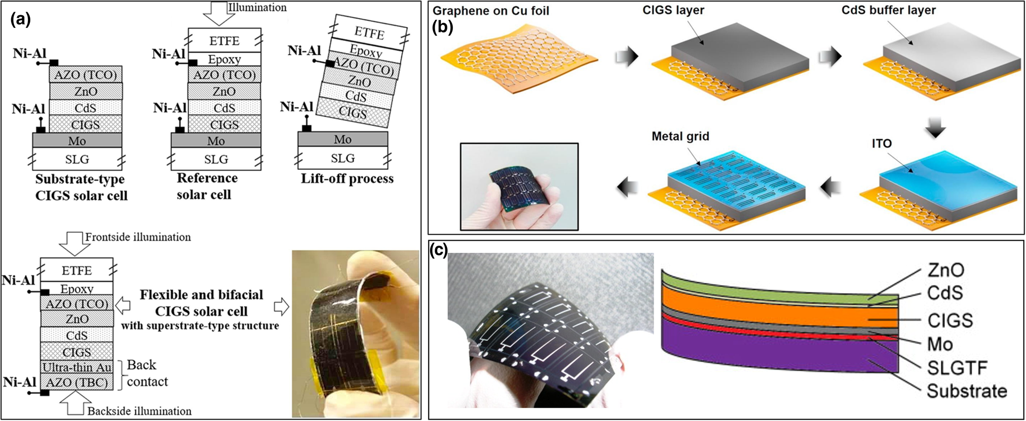
Figure 3. (a) Fabrication method of the flexible and bifacial CIGS solar cell with a superstrate-type structure of ETFE/epoxy glue/AZO/ZnO/CdS/CIGS/ultra-thin Au/AZO transparent back contact (TBC). Reprinted with permission from Ref. Reference Hamada, Nishimura, Chantana, Kawano, Masuda and Minemoto59. (b) Schematic representation of the deposition and fabrication processes of flexible CIGS solar cells on the graphene/Cu foil electrode. Reprinted with permission from Ref. Reference Sim, Kang, Nandi, Jo, Jeong and Lee61 . (c) Picture of a flexible CIGS solar cell fabricated on a zirconia sheet and the corresponding device structure. Reprinted with permission from Ref. Reference Ishizuka, Yamada, Matsubara, Fons, Sakurai and Niki62.
In order to promote inexpensive production of CIGS solar cells, it is essential to develop high efficiency cells over large areas with high yield and high throughput. For commercialization, the devices should exhibit prolonged stability. Nevertheless, flexible cells have several issues including the nonavailability of flexible substrates with suitable chemical, physical, and mechanical characteristics. Metal foils have high roughness, high density, a large thermal coefficient of expansion, as well as impurities which could diffuse to the active layers and degrade cell performance. Nevertheless, metal foils such as copper have been used to develop flexible CIGS cells.Reference Penndorf, Winkler, Tober, Röser and Jacobs60 Graphene-based CIGS cells have been demonstrated on copper foil where graphene was grown on the foil using CVD followed by a direct deposition of the CIGS and active layers onto the graphene, eliminating the need for a transfer process [Fig. 3(b)]. In this case, the graphene acts as a hole transport electrode and the device exhibited an efficiency of 9.91% with a fill factor of 0.647.Reference Sim, Kang, Nandi, Jo, Jeong and Lee61 The reported results are considerably better than those achieved on a reference cell with traditional electrodes.
Another issue with the flexible substrates, particularly polymers, is that they cannot endure high temperatures which are generally needed for growing high-quality films, and consequently, high efficiency cells. It should be noted that polyimide can sustain high temperatures up to 450 °C but only for short durations.Reference Caballero, Kaufmann, Eisenbarth, Unold, Klenk and Schock63 Moreover, while ultra-thin ceramics, such as zirconia [Fig. 3(c)], have been used as flexible substrates they have limited flexiblity which hinders their use in commercial products.Reference Ishizuka, Yamada, Matsubara, Fons, Sakurai and Niki62 Furthermore, the process of forming a graded bandgap in CIGS is accomplished exclusively by tuning the Ga doping, a process currently developed only at high temperatures making it unavailable to temperature-sensitive flexible substrates and thus limiting their performance. Moreover, the CdS buffer layer deposition is achieved via a wet process, and therefore, it is incompatible with R2R production. Finally, R2R manufacturing results in a variation in the polymeric substrate temperature which causes volume expansion.
Commercially, CIGS-based solar cells have been available since 1992 on rigid substrates. More recently, in 2017, leading manufacturers claim commercialization costs below $0.4/Watt.Reference Margolis, Feldman and Boff64 Using flexible substrates could further reduce production and installation costs. Currently, several companies are producing flexible CIGS-based solar cells mainly on stainless steel substrates.Reference Feurer, Reinhard, Avancini, Bissig, Löckinger, Fuchs, Carron, Weiss, Perrenoud, Stutterheim, Buecheler and Tiwari65,Reference Reinhard, Chirila, Blosch, Pianezzi, Nishiwaki, Buecheler and Tiwari66 Misasole demonstrated flexible CIGS cells in 2016 with the efficiency of 19.4% for small modules on the stainless steel substrate,Reference Farshchi, Hickey and Poplavskyy67 while Global Solar has produced CIGS cells on thinner stainless steel substrates in 2017 with the efficiency of 18.7%.Reference Kaczynski, Lee, Alsburg, Sang, Schoop and Britt68 Flisom and Empa are collaborating to provide equipment for manufacturing CIGS cells on polyimide. Even though CIGS sales account for only tens of MW, a small portion compared with Si, flexible CIGS products are becoming more mature with a quickly growing market.
Cadmium telluride thin film
Cadmium telluride (CdTe)-based PV devices are the most produced thin film solar cell worldwide. CdTe exhibits a bandgap of 1.45 eV in its polycrystalline form and 1.5 eV in its monocrystalline formReference Zhao, Boccard, Liu, Becker, Zhao, Campbell, Suarez, Lassise, Holman and Zhang69 which is ideal for achieving a high V oc (theoretically up to 1 V), high J sc (theoretically up to 30 mA/cm), and theoretical efficiency over 27%.Reference Zanio70 Actual CdTe-based devices have shown high efficiencies but only when grown at high temperatures (normally above 500 °C). Since CdTe cannot be deposited at temperatures higher than 350 °C while under vacuum, a controlled atmosphere is needed to enable atom re-evaporation and thus close-space sublimation is used.Reference Sites and Pan71 Nevertheless, growing CdTe at low temperatures results in lower energy consumption, induces less stress in the substrate, and enables the use of various substrates including temperature-sensitive materials needed for the development of flexible cells. CdTe photovoltaic devices can be fabricated using the substrate or the superstrate configurations. The device consists of the substrate, back contact, and buffer layer which is generally based on CdS,Reference Sites, Munshi, Kephart, Swanson and Sampath72 CdTe absorber, and front contact.
The highest efficiencies in CdTe-based solar cells have been achieved using thick absorber layers. However, Te is a scarce material, and therefore, if thick absorbers are needed with high production levels (>20 GW/year), then the availability of the element Te would be a concern. On the other hand, if thinner absorber layers could be used, then this would reduce the cost of the device.Reference Fthenakis73 CdTe has been deposited using radio frequency (RF)-sputtering and with a thickness below 1 μm, an efficiency of 12% was achieved,Reference Paudel, Compaan and Yan74 while thermal evaporationReference Salavei, Rimmaudo, Xu, Barbato, Meneghini, Meneghesso, Di Mare and Romeo75 and close-space sublimation methods have resulted in efficiencies up to 13%.Reference Krishnakumar, Barati, Schimper, Klein and Jaegermann76 Theoretically, an absorber layer with a thickness of 1 μm is enough to capture all the incident light, which was proved by the measured current densities in devices with different absorber thicknesses.Reference Krishnakumar, Barati, Schimper, Klein and Jaegermann76,Reference Paudel, Wieland, Young, Asher and Compaan77 In fact, it has been shown that a thickness of 1.1 μm of sputtered CdTe achieves the maximum density of short circuit current, but when CdTe is evaporated under vacuum requires a thickness of 2 μm, which could be due to the lower density of the material. Moreover, as the devices age, their short circuit current density is shown to increase while their open circuit voltage reduces such that the efficiency is maintained; therefore, good stability is reported in CdTe-based solar cells with thin absorber layers.Reference Paudel, Wieland, Young, Asher and Compaan77 In addition, the recombination in solar cells with ultra-thin CdTe is more pronounced than in the case of thick CdTe-based devices,Reference Kranz, Gretener, Perrenoud, Schmitt, Pianezzi, La Mattina, Blösch, Cheah, Chirilă, Fella, Hagendorfer, Jäger, Nishiwaki, Uhl, Buecheler and Tiwari78 which can be due to the low doping in thin layers that may inhibit the appropriate separation of the fermi levels.
Substrate configuration. Flexible solar cells do not require a transparent substrate and therefore can be fabricated using a wider range of possible substrates. An ideal flexible substrate is Mo due to its excellent stability at increased temperatures, in addition to its good contact with CdTe. The greatest efficiency that was obtained with Mo is 11.5% where the solar cell is grown at low temperatures on a polymeric substrate and sputter coated with Mo/Te as back contact, while doping with Cu post-CdTe deposition achieved 10.9% on a stainless steel substrate.Reference Kranz, Gretener, Perrenoud, Schmitt, Pianezzi, La Mattina, Blösch, Cheah, Chirilă, Fella, Hagendorfer, Jäger, Nishiwaki, Uhl, Buecheler and Tiwari78 Manufacturing CdTe solar cells using a R2R process on metal foils is desired for low production cost. However, most of the CdTe-based solar cells grown on metallic foils had reduced efficiencies (less than 10%) due to the need of inverting the structure which puts limitations on the fabrication methods and results in low-quality CdTe layers.
Doping the CdTe with copper in a controlled manner has been demonstrated as a promising technique where a record efficiency of 13.6% was achieved in an inverted structure. In this case, less than a monolayer of copper is evaporated and annealed to achieve controlled doping of CdTe, which enhances the hole density, carrier lifetime, and carrier collection in the photovoltaic device, as shown in Fig. 4(a).Reference Kranz, Gretener, Perrenoud, Schmitt, Pianezzi, La Mattina, Blösch, Cheah, Chirilă, Fella, Hagendorfer, Jäger, Nishiwaki, Uhl, Buecheler and Tiwari78

Figure 4. (a) Scanning electron micrograph and schematic of the cross-section of a CdTe solar cell in the superstrate configuration (left) and the substrate configuration (right) which allows the use of opaque substrates like metal foils. In substrate configuration, Mo/MoOx and i-ZnO/ZnO:Al are used as electrical back and front contacts, respectively. The scale bars correspond to 1 mm. The yellow arrows show the direction of illumination. Reprinted with permission from Ref. Reference Kranz, Gretener, Perrenoud, Schmitt, Pianezzi, La Mattina, Blösch, Cheah, Chirilă, Fella, Hagendorfer, Jäger, Nishiwaki, Uhl, Buecheler and Tiwari78 . (b) Schematic illustrations for the fabrication of poly-CdS/epi-CdTe and epi-CdS/epi-CdTe flexible solar cells. Reprinted with permission from Ref. Reference Wen, Lu, Sun, Xiang, Chen, Shi, Bhat, Wang, Washington and Lu79. (c) Schematic layout of the CdTe solar cell structure and the image of 3 × 3 cm solar cells fabricated on different substrates. Reprinted with permission from Ref. Reference Salavei, Menossi, Piccinelli, Kumar, Mariotto, Barbato, Meneghini, Meneghesso, Di Mare, Artegiani and Romeo80.
Recently, the majority of the high-quality CdTe were formed on single-crystal substrates via either molecular beam epitaxy (MBE) or metal-organic chemical vapor deposition (MOCVD). As a result, using CdTe in flexible electronics has been rare due to the requirement of the rigid substrate. Most recently, Wen et al. demonstrated the epitaxial growth of high-quality CdTe films on the mica substrate by the vapor transport deposition process through weak interface interactions and achieved an efficiency of 9.59% [Fig. 4(b)].Reference Wen, Lu, Sun, Xiang, Chen, Shi, Bhat, Wang, Washington and Lu79 The transfer of the CdTe film from the mica substrate onto various flexible substrates was also possible due to the weak interfacial interactions. In fact, the epitaxial film was released from the substrate when dipped in water via surface tension, and an SU8 substrate was used as the flexible permanent substrate for the solar cell. As a result, a CdS/CdTe solar cell with both layers being epitaxial exhibited an efficiency of 9.59% with an improved interface quality (low defects) and diode performance comparable to the same device with layers of poly-CdS/epi CdTe [Fig. 4(b)]. The devices showed excellent mechanical resilience where around 96.5% of the initial efficiency is maintained after 1000 bending cycles with a bending radius of 10 mm. Nevertheless, even though the obtained efficiency is lower than previously achieved efficiencies for flexible CdTe-based PV cells, the demonstrated results show that there is room for improving the performance of CdTe solar cells by increasing the carrier lifetime through an enhanced film quality.
Superstrate configuration. Another option for the development of flexible CdTe solar cells is based on the superstrate configuration, which requires the use of transparent substrates that can endure and remain stable at high temperatures during the different fabrication processes [Fig. 4(c)].Reference Salavei, Menossi, Piccinelli, Kumar, Mariotto, Barbato, Meneghini, Meneghesso, Di Mare, Artegiani and Romeo80 The first substrate studied for flexible CdTe-based solar cells using the superstrate configuation was polyimide.Reference Salavei, Menossi, Piccinelli, Kumar, Mariotto, Barbato, Meneghini, Meneghesso, Di Mare, Artegiani and Romeo80,Reference Tiwari, Romeo, Baetzner and Zogg81 Upilex-S and Kapton showed promising resultsReference Romeo, Khrypunov, Kurdesau, Arnold, Bätzner, Zogg and Tiwari82,Reference Perrenoud, Schaffner, Buecheler and Tiwari83 but remain temperature-limited as they cannot withstand temperatures above 450 °C. The highest efficiency obtained is 12.7%, where the CdTe/CdS layers were grown on aluminum-doped ZnO on polyimide.Reference Perrenoud, Schaffner, Buecheler and Tiwari83 Recently, polymer substrates have been replaced with ultra-thin alkali-free glass which is flexible and stable when exposed to high temperatures or chemicals.
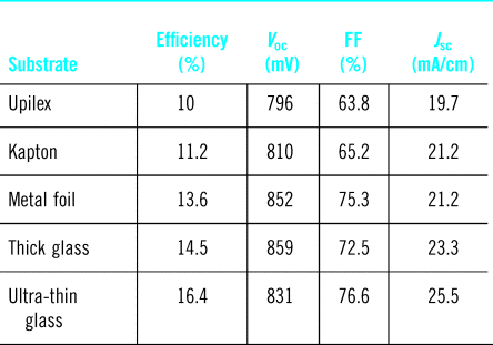
Developing solar cells on glass allows the growth of the active layers at high temperatures. Ultra-thin glass was first used by Rance et al.Reference Rance, Burst, Meysing, Wolden, Reese, Gessert, Metzger, Garner, Cimo and Barnes84 where CdS was deposited by sputter-coating instead of by the wet chemical process. As a result, a record efficiency of 16.4% has been achieved.Reference Mahabaduge, Rance, Burst, Reese, Meysing, Wolden, Li, Beach, Gessert, Metzger, Garner and Barnes85 Moreover, Salavei et al.Reference Salavei, Menossi, Piccinelli, Kumar, Mariotto, Barbato, Meneghini, Meneghesso, Di Mare and Artegiani86 used ultra-thin glass to fabricate CdTe-based solar cells at low temperatures. In this case, the same process was also applied on two polymers, Upilex and Kapton, and the stress generated in the films was studied using XRD. The results showed that the compressive strain is observed in the upper parts of the solar cells fabricated on the polyimides, while the bulk of the solar cell did not show any strain. This was also confirmed by Rance et al.Reference Rance, Burst, Meysing, Wolden, Reese, Gessert, Metzger, Garner, Cimo and Barnes84 where a larger distortion was observed in the CdTe surface. The compressive and tensile stresses generated in CdTe deposited on polyimides and ultra-thin glass have also been analyzed using Raman spectroscopy.Reference Salavei, Menossi, Piccinelli, Kumar, Mariotto, Barbato, Meneghini, Meneghesso, Di Mare and Artegiani86 The obtained results confirmed that the polyimide substrates result in larger distortions in CdTe than the ultra-thin glass substrates which could thus cause a stability issue in CdTe solar cells deposited on flexible polymers compared with glass. Table 2 lists the best efficiencies achieved in flexible CdTe solar cells developed on various substrates. The table shows that the highest efficiency is achieved on ultra-thin glass, while the device developed on Upilex exhibits the lowest efficiency, due to degraded photocurrent density in a lower transparency substrate.
Table 2. Best efficiencies of flexible CdTe devices.
The CdTe photovoltaic device should exhibit prolonged stability regardless of the structure configuration. In general, the CdTe material is very stable when encapsulated using a moisture-resistant material. However, it should be noted that, in the past, there was a stability issue in CdTe solar cells due to the diffusion of copper but was later solved by lowering the copper content and introducing a diffusion barrier at the back contact.Reference Gessert, Romero, Dhere and Asher87–Reference Artegiani, Menossi, Shiel, Dhanak, Major, Gasparotto, Sun and Romeo89 Current CdTe solar cells formed on the glass substrate exhibit excellent stability which enabled the production of large modules. However, regarding flexible CdTe-based solar cells, the stability can be affected by the bending and stretching of the device, and very few researchers have analyzed the stability of flexible cells. Rance et al. studied the impact of tensile and compressive stretching on the performance of flexible cells developed on ultra-thin glass.Reference Rance, Burst, Meysing, Wolden, Reese, Gessert, Metzger, Garner, Cimo and Barnes90 The solar cells were mounted on tubes with different curvatures to study the effect of different bending radii. Similar tests on polymeric substrates have not been conducted; however, since the variation in the measured efficiencies is due to the generated stress in the active layers and not due to the substrate material, it is expected that similar behavior would be observed on polymeric substrates. Another stability issue that arises when using polyimide substrates is deterioration from UV radiation.Reference Kim, Hwang, Namgoong, Kim and Kim91,Reference Green, Hishikawa, Dunlop, Levi, Hohl-Ebinger and Ho-Baillie92 Therefore, the polymeric substrate needs to be coated with a UV-resistant material.
CdTe thin film-based solar cells are currently being mass produced mainly by a single company (First Solar). The high reproducibility and simple stoichiometry minimize any inhomogeneity issues which are more common in other thin film-based solar cells with high efficiency. Nevertheless, since Si wafers are being mass produced, this made the thin film-based modules production costs similar to that of Si modules. However, thin film-based cells can potentially be made lower cost if their ability to adapt to different curvatures is considered. This would enable the integration and substitution of traditional roofs with photovoltaic roofs. The application of CdTe thin films on innovative substrates should be considered especially because it is enormously simple to grow CdTe without being affected by the different employed substrates, with minimized inhomogeneity problems for large area growth, and with a promising potential to be mass produced in flexible shapes. Moreover, CdTe-based solar cells using the superstrate configuration are the simplest to fabricate, and they would be ideal for application on windows and ultra-thin glass while the substrate configuration would be favored on ceramic surfaces and tiles. Nevertheless, the development of low-cost flexible glass and polymer substrates is needed to reduce the cost of CdTe solar cell.
Silicon–germanium and III–V thin film
III–V compound semiconductor photovoltaic devices have exhibited record efficiencies over all other materials. For instance, single-junction GaAs devices have shown efficiencies up to 29.1%, while III–V on Si solar cells exhibited efficiencies as high as 35.5%.Reference Kim, Hwang, Namgoong, Kim and Kim91,Reference Green, Hishikawa, Dunlop, Levi, Hohl-Ebinger and Ho-Baillie92 This is due to the excellent properties of III–V materials in terms of direct bandgap, prolonged stability, radiation hardness, in addition to its ideal optoelectronic characteristics. Even though the expensive cost of the wafer has been a bottleneck for deploying this technology at large, several works have reported the fabrication of flexible III–V solar cells where the substrate was back etched to thin it down. For instance, 80-μm-thick triple-junction PV cells (CTJ30-80) were developed by CESI for use in space with an InGaP/InGaAs/Ge epitaxial structure. Metal organic CVD was used to grow the epitaxial structure, a tool that can simultaneously receive up to 13 germanium substrates during each run. The active layers of the solar cell were formed on 100-mm-diameter and 140-μm-thick Ge substrates. Once the epitaxial growth is completed, the Ge substrate is back etched to reach a final thickness of around 80 μm. Using this technique, an efficiency of 29% is achieved under 1 sun.Reference Campesato, Gabetta, Lisbona and D'Abrigeon93
Over time, many efforts have been made to discover solutions to reduce the cost of manufacturing flexible III–V solar cells. In fact, the major expense in III–V cells comes from the costly crystalline III–V wafers which are needed to grow the epitaxial layers. To overcome this, epitaxial lift-off and transfer methods have been established,Reference Yablonovitch, Gmitter, Harbison and Bhat94–Reference Yoon, Jo, Chun, Jung, Kim, Meitl, Menard, Li, Coleman, Paik and Rogers98 and a record 28% efficiency flexible solar cell based on single-junction GaAs has been demonstrated using this technique.Reference Kayes, Nie, Twist, Spruytte, Reinhardt, Kizilyalli and Higashi99 In this method, the active layers are epitaxially grown on a crystalline wafer and then lifted off and transferred onto a permanent substrate while the original costly wafer can be reused for other runs. Another approach was based on mechanical bonding.Reference Cariou, Benick, Feldmann, Höhn, Hauser, Beutel, Razek, Wimplinger, Bläsi, Lackner, Hermle, Siefer, Glunz, Bett and Dimroth100 Nevertheless, the potential scalability of the process and the cost effectiveness of these techniques are still vague. In fact, it can be concluded from the current low-market size of III–V solar cells that there is not enough cost benefits to make this technology competitive with the existing solar cell technologies including Si, CIGS, and CdTeReference Fu, Feldman, Margolis, Woodhouse and Ardani101,Reference Woodhouse and Goodrich102 for terrestrial applications.
In order to reduce the costs of III–V solar cells, it is essential to develop a scalable process for manufacturing. One solution would be to directly deposit the active layers of the III–V device onto inexpensive substrates which can be either flexible or can be used as sacrificial substrates. However, it is essential to find inexpensive substrates that have lattice match with the III–V material and can endure high temperatures. For example, the growth of GaAs was reported on a low-cost monocrystalline silicon wafer via a SiGe buffer layer with graded composition to avoid misfit defects between GaAs and Si.Reference Jain and Hudait103–Reference Cariou, Benick, Beutel, Razek, Flotgen, Hermle, Lackner, Glunz, Bett, Wimplinger and Dimroth105 The largest efficiency obtained with single-junction GaAs/Si was 18.1% which was limited due to the high density of threading dislocations.Reference Andre, Carlin, Boeckl, Wilt, Smith, Pitera, Lee, Fitzgerald and Ringel106–Reference Wang, Ren, Thway, Lee, Yoon, Peters, Buonassisi, Fizgerald, Tan and Lee109 Nevertheless, the use of thick buffer layers increased the cost of the device making them commercially unfeasible. Another method is based on the selective area growth of high-quality III–V layers without the need for thick buffer layers.Reference McClelland, Bozler and Fan110–Reference Warren, Makoutz, Horowitz, Dameron, Norman, Stradins, Zimmerman and Tamboli112 Using this technique, an efficiency of 10.4% has been achieved in GaAs grown on patterned silicon with V-grooves.Reference Vaisman, Jain, Li, Lau, Makoutz, Saenz, McMahon, Tamboli and Warren113 Another method is based on the growth of GaAs on polycrystalline Ge substrates where good efficiencies were achieved; however, the cost effectiveness was negligible.Reference Venkatasubramanian, O'Quinn, Hills, Sharps, Timmons, Hutchby, Field, Ahrenkiel and Keyes114,Reference Venkatasubramanian, O'Quinn, Siivola, Keyes and Ahrenkiel115 Moreover, GaAs-based solar cells have been demonstrated where the GaAs was grown on polycrystalline substrates with large grains, including Ge, Mo, and W/graphite.Reference Wilt, Smith, Maurer, Scheiman and Jenkins116,Reference Polly, Plourde, Bailey, Leitz, Vineis, Brindak, Forbes, McNatt, Hubbard and Raffaelle117 However, only low efficiencies were obtained (around 10%) due to the polycrystalline nature of GaAs with grain boundaries and defects acting as recombination centers.Reference Kurtz and McConnell118
In order to obtain high-quality, single crystal-like layers on nonepitaxial wafers, a new technique has been demonstrated (seed-and-epitaxy) where very thin seed films with a single crystal-like structure are used as the substrate for growing the GaAs layer.Reference Wilt, Smith, Maurer, Scheiman and Jenkins116,Reference Teplin, Ginley and Branz119 In fact, single crystal-like Ge seed films were demonstrated on amorphous glass and polymetal via the ion beam-assisted deposition (IBAD) method. If GaAs-based solar cells could be grown on low cost metal substrates via a continuous R2R manufacturing process, then there would be a chance to merge high efficiency with low cost. In this light, Dutta et al. recently developed a R2R plasma-enhanced chemical vapor deposition method to form high-quality Ge films with a single crystalline-like structure on flexible metallic substrates. IBAD was employed to achieve templates with a single crystalline-like structure to allow the epitaxial growth of Ge thin films [Fig. 5(a)]. The Ge film on metal foil substrates was then employed to grow flexible GaAs single-junction PV cells using the MOCVD which exhibited efficiencies up to 11.5%.Reference Dutta, Rathi, Khatiwada, Sun, Yao, Yu, Reed, Kacharia, Martinez, Litvinchuk, Pasala, Pouladi, Eslami, Ryou, Ghasemi, Ahrenkiel, Hubbard and Selvamanickam120
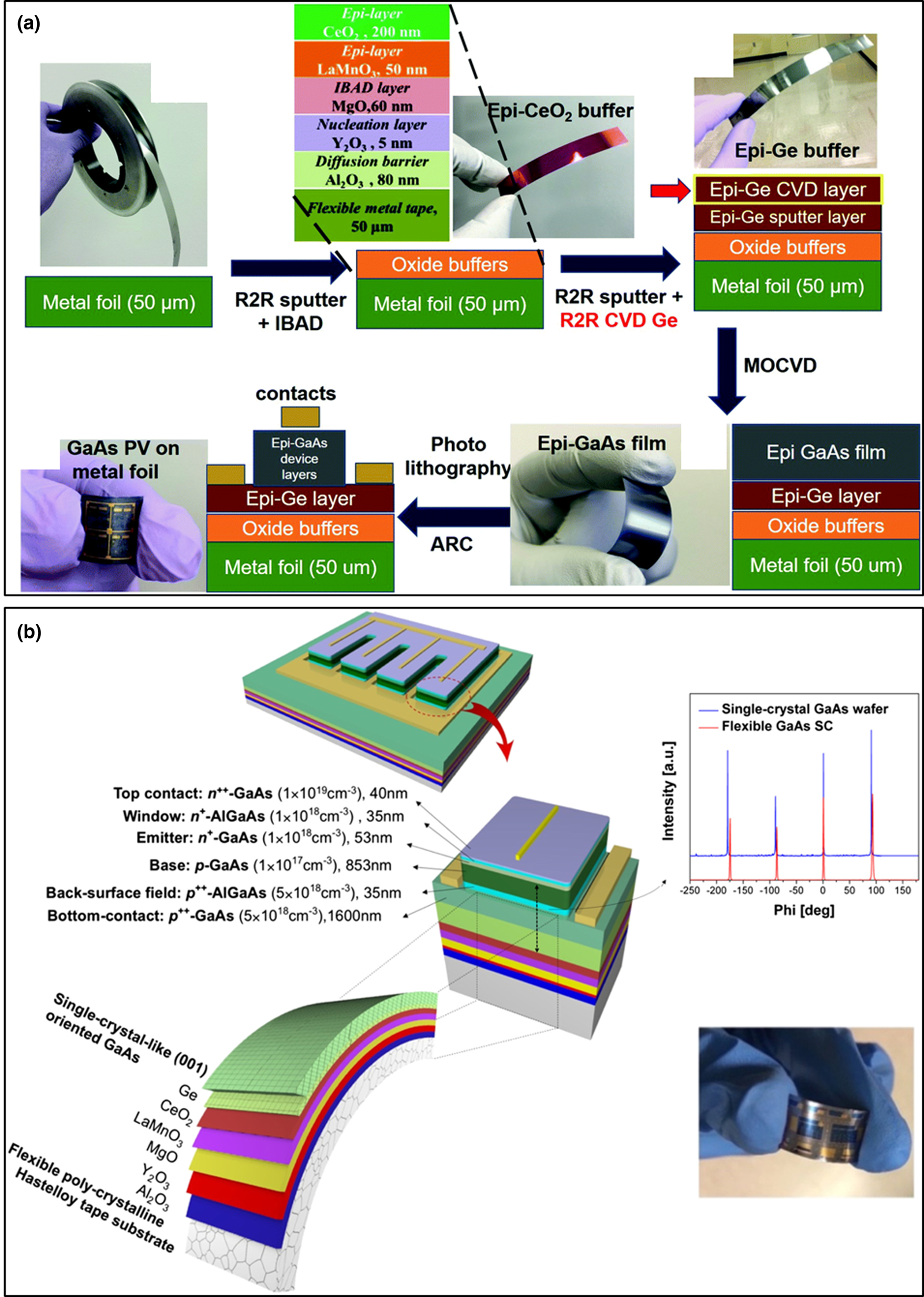
Figure 5. (a) Schematic of a fabricated single-junction (SJ) GaAs solar cell on a CVD-Ge template on metal foil and a photograph of a flexible SJ solar GaAs solar cell are shown. Reprinted with permission from Ref. Reference Dutta, Rathi, Khatiwada, Sun, Yao, Yu, Reed, Kacharia, Martinez, Litvinchuk, Pasala, Pouladi, Eslami, Ryou, Ghasemi, Ahrenkiel, Hubbard and Selvamanickam120. (b) Schematic illustration of the device and layer structures of flexible high-efficiency photovoltaic solar cells (PVSCs). The XRD φ scan around the epitaxially grown GaAs (224) peak demonstrates four sharp peaks 90° apart with in-plane texture spread of 1.2° showing a well comparable structure with single-crystal GaAs wafer. Reprinted with permission from Ref. Reference Pouladi, Rathi, Khatiwada, Asadirad, Oh, Dutta, Yao, Gao, Sun, Li, Shervin, Lee, Selvamanickam and Ryou121.
Pouladi et al. were the first to develop flexible single-junction III–V photovoltaic devices based on GaAs thin film with the single crystal-like structure [Fig. 5(b)]. The film was formed on a low-cost metal tape by direct deposition. The device exhibited a promising efficiency of 7.6%.Reference Pouladi, Rathi, Khatiwada, Asadirad, Oh, Dutta, Yao, Gao, Sun, Li, Shervin, Lee, Selvamanickam and Ryou121 This leads to overcoming the high-cost single crystal wafer fabrication challenge. Moreover, the devices showed negligible degradation when bent up to 100 cycles with a bending radius of 0.5 cm in both convex and concave modes.
Inorganic perovskite thin film
Perovskite-based solar cells were first demonstrated in 2009 where an efficiency of 3.8% was achieved.Reference Kojima, Teshima and Shirai122 Later, in 2017, Zhou et al. enhanced the efficiency up to 19.3%.Reference Zhou, Chen and Li123 The efficiency of perovskite-based solar cells have been continuously improving since then and currently, the world record efficiency is 25.2%.124,Reference Kojima, Teshima, Shirai and Miyasaka125 Even though the efficiencies of the hybrid perovskite solar cells are similar to the commercial ones, they are unstable, which inhibits their actual commercialization.Reference Li, Zhu, Li, Jen and Wang126, Reference Jiang, Feng, Zhao, Li, Yin, Han, Yan, Liu and Liu127 An alternative approach is to use all inorganic cesium-based perovskite material that exhibits enhanced moisture, light, and thermal stability.124 In Pb-halide perovskites, CsPbI3 shows a bandgap of 1.73 eV which is suitable for application in solar cells. However, the CsPbI3 is stable in the cubic phase only at increased temperatures, and at room temperature humid environments goes back to the orthorhombic phase, with a bandgap of 2.82 eV. As a result, a low efficiency of only 0.09% was achieved with the orthorhombic phase of perovskites with bad stability.Reference Choi, Jeong, Kim, Kim, Walker, Kim and Kim128
In the last 2 years, perovskite-based cells have improved quickly. In fact, until 2015, Snaith and coworkers used the inorganic CsPbI3 with small grain size (after treatment with hydriodic acid) and reported an efficiency of 2.9%.Reference Eperon, Paternò, Sutton, Zampetti, Haghighirad, Cacialli and Snaith129 In 2016, Luther and coworkers reported that CsPbI3-based quantum dots exhibit prolonged stability at room temperature and in a humid environment where the cubic phase can be maintained for months. As a result, an efficiency of over 10% was achieved.Reference Swarnkar, Marshall, Sanehira, Chernomordik, Moore, Christians, Chakrabarti and Luther130 Since then, multiple techniques have been studied to enhance the stability of the inorganic perovskite material with cubic phase by minimizing its grain size, including polymer modification,Reference Hu, Bai, Liu, Ji, Miao, Qiu and Zhang131 ion doping,Reference Li, Zhang, Fu, Yu, Zhou, Zhang and Yin132 and dimension control.Reference Jiang, Yuan, Ni, Yang, Wang, Jiu, Yuan and Chen133 However, passivating the grain boudaries becomes essential as more grain boudaries will exist when smaller grain sizes are achieved.Reference Zhang, Bai, Jin, Bian, Wang, Sun, Wang and Liu134 In 2018, Wang and coworkers reported a distorted black CsPbI3 film using additives including hydroiodic acid (HI) and phenylethylammonium iodide (PEAI). It is shown that the HI produces hydrogen lead iodide (HPbI3+x), which represents a transition to the distorted black phase with a band gap of 1.69 eV; whereas PEAI leads to nucleation which is needed to achieve an optimized crystallization. More notably, the additive stabilizes the distorted black phase where the phase transition is obstructed due to its steric effects. As a result, high efficiencies up to 15.07% were reported with a negligible loss after 300 h of light exposure (without encapsulation). The devices showed good stability as well where 92% of its initial cell efficiency was maintained after a 2-month storage under ambient conditions.Reference Wang, Jin, Liang, Bian, Bai, Wang, Zhang, Wang and Liu135 More recently, in 2020, Zhang et al. synthesized black-phase CsPbI3 perovskite thin films with good quality and stability using an antisolvent-based blended with a methylammonium iodide mediator. As a result, smaller perovskite crystallites were developed with enhanced stability, morphology, and photoelectronic characteristics. Efficiencies of >16% were obtained which good reproducibility and stability where 95% of the initial efficiency is maintained after 1000 h.Reference Zhang, Wang, Chen, Ji, Wang, Li, Raschke and Li136
Snaith and coworkers reported, in 2016, the stability of cesium lead mixed-halide perovskites (CsPbI2Br) in its cubic phase at room temperature even when bulk material is used.Reference Sutton, Eperon, Miranda, Parrott, Kamino, Patel, Hörantner, Johnston, Haghighirad, Moore and Snaith137 This material shows a bandgap range between 1.82 and 1.92 eV, which depends on the growth technique. The cubic phase stability was improved due to the reduced temperature of phase transition. As a result, the first solar cell based on CsPbI2Br exhibited an efficiency of 9.8%,Reference Sutton, Eperon, Miranda, Parrott, Kamino, Patel, Hörantner, Johnston, Haghighirad, Moore and Snaith137 which quickly improved to 14.8% most recently due to the enhancements in grain boundary passivation, crystal morphology control, structure optimization, and interface engineering.Reference Yan, Xue, Liu, Zhu, Tian, Li, Chen, Chen, Yan, Yip and Cao138 Nevertheless, even though the achieved stability with the all-inorganic perovskites is considerably better than that of the hybrid perovskites, their efficiencies are still lower. This confirms the need for optimizing the doping density, energy-level matching, in addition to improving the carrier transport and collection to achieve higher J sc and reduce energy loss.
In fact, the deposition of high-quality CsPbI2Br film is challenging, chiefly due to the limited solubility of CsBr. Thus, control over the crystallization throughout the deposition process of the film is important for achieving high-performance CsPbI2Br perovskite solar cells. Different techniques have been studied for this purpose, including a single-step method which resulted in high-quality film but with limited thickness. By controlling the annealing temperature, a 9.5% stabilized power output was achieved; however, the J sc was limited due to the small thickness of the film. To increase the thickness of the film, dimethyl sulfoxide has been added as a co-solvent to increase the solubility of CsBr. This resulted in films with thicknesses above 500 nm. Additionally, CsPbX3 perovskites normally require preparation at high temperature; in fact, annealing temperatures >250 °C are generally needed to achieve the desired photovoltaic active perovskite phase of α-CsPbI2Br. This makes it difficult for the development of flexible solar cells on polymeric substrates. To overcome this, Wang et al.Reference Wang, Zhang, Xu, Li and Zhao139 demonstrated a simple formation of high-performance CsPbI2Br perovskite solar cell by applying a one-step technique and a low temperature annealing process at 100–130 °C. This easily formed CsPbI2Br film exhibited long-term phase stability at room temperature for a period of a month and showed thermal stability at annealing temperatures below 100 °C for over 7 days. As a result, the all-inorganic perovskite solar cell achieved efficiencies up to 10.56%. In addition, Hu et al.Reference Hu, Zhang, Shu, Qiu, Bai, Ruan and Xu140 developed a vacuum-assisted drying process for the fabrication of all-inorganic perovskite films at room temperature [Fig. 6(a)]. The photoelectric characteristics and morphology of the film, in addition to the long-term stability, are considerably enhanced in comparison to those of the reference layer developed with the assistance of the annealing process. The obtained flexible cells using the room temperature processed films exhibited a high efficiency of 11.47% with a negligible hysteresis.Reference Hu, Zhang, Shu, Qiu, Bai, Ruan and Xu140 Moreover, the devices maintained 95% of the original efficiency when bent down to 4.5 mm bending radius up to 200 cycles. Rao et al. also demonstrated the development of inorganic perovskite thin films at room temperature using a dimethylsulfoxide solvent annealing treatment. This technique is found to enable control over the crystallization process of the thin film resulting in uniform and hole-free layers [Fig. 6(b)]. Consequently, an efficiency of 6.4% in a (indium tin oxide, ITO)/NiOx/RT-CsPbI2Br/C60/Bathocuproine (BCP)/Ag device is demonstrated and was further improved to 10.4% through post-annealing at an optimal temperature of 120 °C. Finally, the authors developed a flexible perovskite solar cell using this technique which exhibited an efficiency of 7.3%.Reference Rao, Ye, Gu, Zhao, Liu, Bian and Huang141 The device showed negligible degradation in the efficiency when bent down to 10 mm bending radius up to 100 cycles. More recently, in 2019, Wang et al. showed that the incorporation of 5% of Br ions into the CsPbI3 film resulted in a mixed-halide CsPbI2.85Br0.15 thin film. Using this layer as the absorber layer in a perovskite solar cell, a record reverse scan efficiency is achieved of 17.17% with a stabilized efficiency of 16.83%. Moreover, the authors demonstrated the development of the cell on large-scale and flexible substrates (1 cm), and a record efficiency of 13.14% was reported. In fact, the Br is found to suppress bulk trap-assisted nonradiative recombination and to relax lattice strain which also lead to a good stability where the efficiency dropped by 80% when exposing it to 40–50% relative humidity for 5 h.Reference Wang, Bian, Jin, Zhang, Liang, Wen, Wang, Ding and Liu142

Figure 6. (a) Schematic diagram of the vacuum-assisted drying approach to deposit the all-inorganic perovskite films. Reprinted with permission from Ref. Reference Hu, Zhang, Shu, Qiu, Bai, Ruan and Xu140. (b) Schematic diagram of preparation procedures of the CsPbI2Br films with RT DMSO vapor annealing and direct thermal annealing. Reprinted with permission from Ref. Reference Rao, Ye, Gu, Zhao, Liu, Bian and Huang141.
Low-dimensional material
Even though various low-dimensional materials, such as quantum dots, have been used on solar cells to enhance light trapping,Reference Chowdhury, Alnuaimi, El-Atab, Nayfeh and Nayfeh143–Reference El-Atab, Saadat, Saraswat and Nayfeh149 in this section, we focus on low-dimensional materials that have been used specifically as active layers in the solar cell.
In fact, low-dimensional materials have several benefits, including a large surface area-to-volume ratio, flexibility, enhanced charge collection,Reference Kayes, Atwater and Lewis150 and the potential of improving light absorption via light trapping,Reference Cao, Park, Fan, Clemens and Brongersma151 which make them the focus of research for improving the power conversion efficiency in solar cells. For instance, Jia et al. demonstrated the growth of Ge QDs using a PECVD process which is compatible with the solar cell development process [Fig. 7(a)].Reference Jia, Fan, Zi, Ren, Liu, Liu and Liu152 The quantum dots (QDs) size was optimized to result in the largest solar cell efficiency. In fact, the 14-nm QDs, showing quantum confinement effects, enhanced the short circuit current and efficiency by 8.31%.Reference Jia, Fan, Zi, Ren, Liu, Liu and Liu152 Du et al. developed flexible quantum dot-sensitized solar cells (QDSCs) using a titanium (Ti) mesh which is based on QDs with the desired photovoltaic (PV) performance. ZnO/ZnSe/CdSe nanocrystals were formed on a flexible Ti mesh substrate with the role of photoanodes.Reference Du, Liu, Li, Chen and Zhong153 The nanocrystals were fabricated by surface selenization of ZnO nanosheets to form ZnO/ZnSe core/shell nanostructures. This was followed by a partial conversion of ZnSe to CdSe via the ion replacement method. As a result, an efficiency of 5% was achieved under 1 sun.

Figure 7. (a) Schematics of the a-SiGe:H solar cell with Ge-QDs and its corresponding external quantum efficiency (EQE) measurement. Reprinted with permission from Ref. Reference Jia, Fan, Zi, Ren, Liu, Liu and Liu152. (b) Solar cell fabrication graphene-insulator-silicon (GIS) cell schematic showing the steps for forming the backside contact, electroplating, exfoliating, interlayer Al2O3 deposition, graphene/PMMA transfer, and frontside contact. Reprinted with permission from Ref. Reference Ahn, Chou and Banerjee154.
In terms of 2D materials, graphene has gained a lot of interest in the past years,Reference El-Atab, Turgut, Okyay, Nayfeh and Nayfeh155–Reference Nayfeh, Okyay, El-Atab, Cimen and Alkis157 and for photovoltaics in specific, several of its physical chracteristics are exceptionally attractive, including the high electrical conductivity, mechanical flexibility, and transparency. Therefore, researchers have considered graphene for enhancing the performance of solar cells. To this end, Ahn et al. developed a graphene–insulator–silicon solar cell with an Al2O3 insulator layer. The device is fabricated on thin foils where the graphene is used as the top contact due to its electrical conductivity and optical transparency. Graphene layers were initially grown by CVD on copper–nickel foils and doped with gold nanoparticles to achieve the p-doping. Finally, the device was encapsulated using poly(methyl methacrylate) (PMMA) which exhibited great stability with negligible performance drop over a period of 30 days under ambient conditions. The flexible silicon thin film was developed using a kerf-less exfoliation approach via spalling. The Al2O3 insulator layer is used as a tunneling barrier for holes in addition to its role as a passivation layer to enhance the minority carrier lifetime from 2 to 27 μs [Fig. 7(b)]. Using this approach, a solar cell with a 7.4% efficiency is achieved.Reference Ahn, Chou and Banerjee154 In addition, Li et al. have reported a solar cell with a similar efficiency (7.5%) using carbon nanotubes. In specific, single-walled carbon nanotube/Si (p–n) solar cells are developed via scalable room temperature processes.Reference Li, Mariano, McMillon-Brown, Huang, Sfeir, Reed, Jung and Taylor158
Bulk silicon
Flexible photovoltaic cells based on crystalline silicon with enhanced efficiency are very promising thanks to the exceptional carrier transport characteristics in c-Si. Even though sub-50-μm-thick Si shows flexural rigidity, two main challenges that arise include an increased mechanical fragility and reduced light absorption. In fact, most of the commercially available c-Si-based solar cells use a 170–250-μm Si substrate. This is because Si with thickness below 50 μm becomes very challenging to handle during the fabrication process, especially at the wafer scale, which makes the development process more costly. In addition, due to the indirect bandgap of silicon, the absorption of light needs phonons support. As a result, in very thin silicon, the absorption of light is significantly reduced leading to a reduction in the power output. These two challenges further increase the $/W for ultra-thin flexible crystalline silicon.
To overcome these challenges, Bahabry et al. and El-Atab et al. demonstrated ultra-flexibility in thick (170 μm) monocrystalline silicon using a corrugation approach.Reference Bahabry, Kutbee, Khan, Sepulveda, Wicaksono, Nour, Wehbe, Almislem, Ghoneim, Torres Sevilla, Syed, Shaikh and Hussain159,Reference El-Atab, Babatain, Bahabry, Alshanbari, Shamsuddin and Hussain160 The corrugation technique is applied on large-scale commercial grade monocrystalline silicon solar cells with interdigitated back contacts (IBC) as shown in Fig. 8. Deep reactive ion etching is used to create grooves within the solar cell until the back contacts are exposed which achieves flexibility through the IBC grid with no deterioration in the original efficiency. Bahabry et al. used kapton tape with linear patterns as the hard mask material which was manually placed on the solar cell. As a result, wide grooves are achieved which resulted in the world record minimum bending radius of 140 μm with an efficiency of 17%. A negligible degradation in the efficiency is observed when bending the cells up to 1000 cycles with a bending radius of 4.5 cm in both convex and concave modes. However, due to the linear patterns, only flexing in one direction was possible.Reference Bahabry, Kutbee, Khan, Sepulveda, Wicaksono, Nour, Wehbe, Almislem, Ghoneim, Torres Sevilla, Syed, Shaikh and Hussain159 El-Atab et al. used kapton tape as the hard mask as well; however, the mask was patterned using the CO2 laser. As a result, different patterns were studied including honeycomb and diamond. The results show that the flexing capability in terms of minimum bending radius, flexing directionality, specific weight, and active area loss can be tuned to meet the different application requirements. The technique is shown to achieve ultra-flexibility in 19% efficient cells. Moreover, the minimum bending radius is shown to depend on the corrugation pattern, for instance, with the diamond patterns, the cells can be bent down to 5 mm up to 500 cycles with negligible degradation in the efficiency.Reference El-Atab, Babatain, Bahabry, Alshanbari, Shamsuddin and Hussain160 The corrugated solar cells also showed enhanced thermal dissipation compared with conventional flat cells as a result of the increased surface area to volume ratio. The devices were also encapsulated using polydimethylsiloxane (PDMS) which resulted in a robust performance under different environmental conditions such as rain, acid rain, and snow exposure. It is worth to note that up till now the IBC technology can provide efficiencies up to 26%; therefore, the corrugation technique promises the realization of flexible monocrystalline silicon solar cells with efficiencies up to 26%. Nevertheless, it should be noted that the actual power output is reduced compared with the original rigid cell due to the loss of active silicon area in the etched grooves (Fig. 8). The corrugation approach is also found to enhance the thermal dissipation in the solar cells by natural convection due to the increased surface area to volume ratio.

Figure 8. Fabrication process flow of the corrugated flexible solar cells. Optical and microscope images of the interconnected Si islands show that grooves are created in Si until the back contacts are exposed. The flexible solar cells can be flexed in different directions based on the corrugation patterns. Reprinted with permission from Refs. Reference Bahabry, Kutbee, Khan, Sepulveda, Wicaksono, Nour, Wehbe, Almislem, Ghoneim, Torres Sevilla, Syed, Shaikh and Hussain159,Reference El-Atab, Babatain, Bahabry, Alshanbari, Shamsuddin and Hussain160.
Stretchable solar cells
While flexibility in solar cells can be realized by thinning down the active layers such that the produced strain is below the fracture limit of the material, however, stretchability involves the change of material size which may be reversible in addition to potential out-of-plane deformations. Therefore, achieving stretchability in solar cells needs to be tackled differently. Semiconductor-based solar cells show higher efficiencies than their organic counterpart; however, they are inherently rigid and brittle. To overcome these constraints, three different techniques have been demonstrated to achieve stretchable inorganic solar cells. The first approach is based on the development of various forms of shape engineering such as wavy, serpentine, and stiff-island structures,Reference Zhang, Xu, Fu, Lee, Su, Hwang, Rogers and Huang161–Reference Kim, Ahn, Choi, Kim, Kim, Song, Huang, Liu, Lu and Rogers163 which enable stretching as a result of various mechanisms, including out-of-plane deformation, twisting, and buckling.Reference Bowden, Brittain, Evans, Hutchinson and Whitesides164 The first inorganic material-based stretchable solar cell was demonstrated in 2011 by Rogers and coworkers where single-junction GaAs cells with the small area (3.6 μm-thick) were transferred onto a prestrained elastomer which included interconnects that are downward buckled [Fig. 9(a)]. As a result, an efficiency of ~13% with stretchability up to 20% was achieved with a robust mechanical performance up to 500 cycles.Reference Lee, Wu, Shi, Yoon, Park, Li, Liu, Huang and Rogers165 In a follow-up work, ultra-thin with optimized geometry microcells based on dual-junction GaInP–GaAs were used to show a 19% efficiency and 60% stretchability but with a 33% loss of active area.Reference Lee, Wu, Ryu, Liu, Meitl, Zhang, Huang and Rogers166 Nevertheless, the demonstrated inorganic material-based stretchable solar cells require a transfer process with the excellent alignment of the ultra-thin and patterned inorganic III–V material from the parent wafer onto the permanent prestrained elastomer, with great adhesion and negligible alignment mismatch.Reference Nam, Lee, Choi, Kim, Kim, Kim, Kim and Jo167

Figure 9. (a) Development of the stretchable GaAs solar cell where the array of ultra-thin GaAs microcells is bonded onto a prestrained, structured substrate of PDMS. Reprinted with permission from Ref. Reference Lee, Wu, Shi, Yoon, Park, Li, Liu, Huang and Rogers165. (b) Schematic illustration for stretchable vertical array of Si wires array embedded into an elastomer, PDMS. Reprinted with permission from Ref. Reference Yoon and Khang168. (c) Fabrication process flow of the stretchable solar cells. Inset shows SEM cross-section of the solar cell and the IBC structures connecting two silicon islands. The optical images of the stretchable solar cell before stretching and after stretching by ~33% are shown. Reprinted with permission from Ref. Reference El-Atab, Qaiser, Bahabry and Hussain169.
The second technique is based on the development of organic/inorganic solar cells where silicon microwire-based solar cells are encapsulated in an elastomer, such as PDMS. Yoon and Khang demonstrated a stretchable solar cell based on an array of vertical Si micropillars embedded into the PDMS elastomer as depicted in Fig. 9(b).Reference Yoon and Khang168 The cell has the capability to be stretched reversibly up to 100% with no obvious performance deterioration. In addition, the solar cell can be converted into a bifacial cell by using stretchable Ag nanowire electrodes. Nevertheless, the achieved efficiency with this technique is low (3.3%). In addition, this technique requires the preparation of an ordered array of silicon microwires; otherwise, a variation in the performance from cell-to-cell would be observed.
Thirdly, El-Atab et al. used the corrugation technique to demonstrate an ultra-stretchable solar cell in thick (170 μm) monocrystalline silicon cell with the IBC technology.Reference El-Atab, Qaiser, Bahabry and Hussain169,Reference El-Atab, Shamsuddin, Bahabry and Hussain170 The method is based on the patterning of the hard mask such that islands are obtained which are readily interconnected via the IBC grid [Fig. 9(c)]. The different patterns are shown to enable different stretching capabilities where the stretchability is achieved by orthogonally aligning the rigid islands to the applied tensile stress in addition to employing an Ecoflex elastomer as a stretchable substrate. The achieved mechanics guarantee that the brittle rigid islands do not experience substantial mechanical stress during the stretching process. Using this approach, a world record in stretchability of inorganic solar cells is achieved (95%) with a world record efficiency (19%) and an excellent mechanical resilience up to 500 cycles. It is worth to note again that the IBC technology has enabled efficiencies up to 26% up till now; thus, this approach can lead to ultrastretchable silicon cells with similar efficiencies. Moreover, the corrugation technique is shown to enhance the thermal dissipation by natural convection. It is also important to note that the corrugation approach enables both in-plane and out-of-plane stretching capabilities which can further widen the range of its applications. Nevertheless, due to the common electrodes at the edges of the IBC grid and due to the linear patterns in the grid, stretching was only possible in one direction – perpendicularly to the IBC lines. However, designing an IBC grid with different fractal patterns in the future, such as the serpentine design, could achieve ultra-stretchability in multi-directions. In terms of commercial status, no stretchable solar cell is currently being produced by any manufacturer probably due to the lack of a wide range of applications. However, in recent years, wearables and foldables have gained a lot of interest, and to make these systems self-powered, stretchable energy-harvesting devices must be integrated for which stretchable solar cells would be one promising option. In specific, the corrugation technique is simple and can be applied on large-scale commercial grade solar cells, and therefore, it holds promises for potential future commercialization.
Encapsulation
Flexible solar cells need to be encapsulated using a transparent layer with a low water vapor transmission rate. Moreover, they have to protect the plastic substrate (in case, plastic is used as the substrate) from UV radiation as well as being UV-resistant themselves. Generally, a polymeric encapsulation is employed including polyvinyl fluoride films, Teflon ethylene tetrafluoroethylene or “EVA” resin encapsulant; however, these increase the cost of the module. Multilayers of organic/inorganic films have been used to address this issue such as the CVD-deposited stack of a-SiNx/PGMA/a-SiNx (PGMA stands for poly(glycidyl methacrylate)) with a low water vapor transmission rate,Reference Spee, van der Werf, Rath and Schropp171 in addition to other options including atomic layer-deposited Al2O3,Reference Ali, Choi, Jo and Lee172 sputtered SiOx, Reference Bang, Hwang and Kim173 and silica-like layer deposited using PECVD.Reference Elam, Starostin, Meshkova, van der Velden-Schuermans, Bouwstra, van de Sanden and de Vries174 Finally, the curing process or the deposition temperature of the different encapsulants needs to be below the glass transition temperature of the substrates and thus not all substrates are compatible with the listed encapsulants. For instance, EVA resin is usually cured at 220 °C,Reference Seymour175 which is above the glass transition temperature of flexible plastic substrates (PET and PEN) of 150–200 °C, thus, in this case, employing an encapsulant which can be cured at lower temperatures is necessary (e.g. PDMS).
It should be noted that the flexible solar cells based on plastic substrates exhibit high water vapor transmission rates and gas permeation, unlike rigid cells which are encapsulated in glass with an ultra-low water vapor transmission rate. The flexible devices developed on metal foils show this benefit only on the metallic side, while the other side still has to be encapsulated with a flexible layer that shows high transparency and a low water vapor transmission rate. Currently, the encapsulation of flexible cells with polymers makes the resulting module very costly. Thus, more efforts need to be made to develop low cost polymers which show excellent transparency, low water vapor transmission rates, good stability, and UV resistance.
Outlook and conclusion
In this review, the achieved advancements and current progress in the areas of inorganic material-based flexible and stretchable photovoltaic devices have been highlighted with a focus on various practical aspects and up to date industrial data. Flexible solar cells can be divided into three main categories based on the type of inorganic material used, including thin films, low-dimensional materials, and bulk material.
Thin film-based solar cells are advantageous when used in large modules thanks to the smallest loss in efficiency with upscaling, in addition to the simple monolithic integration when compared with other technologies. Nevertheless, the mass production of silicon wafers reduces the cost of silicon-based modules and keeps thin film-based modules at a competitive disadvantage. However, flexible thin film-based solar cells promise further cost reduction if developed on a wider range of substrates as they could be more easily integrated, on roofs and buildings for instance.
Flexible a-Si thin film-based solar cells have a wide range of application from space, medical application, agriculture, textiles to outdoor utility. In addition to niche applications, the market growth of flexible a-Si-based solar cells will depend on the encapsulation material cost, warranty, and stability of the efficiency under different mechanical and environmental conditions.
CIGS thin film solar cells provide the best efficiencies and mature technology for conventional applications. The achieved efficiency is larger than that of organic cells, and unlike inorganic perovskites, instability, and toxicity are minor. As a matter of fact, currently produced flexible CIGS modules compete with the polycrystalline Si-based modules in terms of efficiency. Flexible CIGS solar cells can be further improved when a wider range of substrates that can sustain high temperatures can be developed, which is needed to fabricate high-quality CIGS thin films. Currently, the transfer approach looks promising since the impact of high temperature can be mitigated.
Flexible CdTe thin film-based solar cells are currently being mass produced due to their promising performance and excellent reproducibility. They can be further improved when a wider range of viable substrates are available, innovative buffer layers could be introduced to mitigate impurity diffusion from the substrate, novel back contacts with improved stability to the fabrication processes can be developed, and enhanced doping methods can be applied to improve the electrical performance of the cells. In addition, more testing to determine the stability of flexible CdTe solar cells during and after bending should be conducted.
III–V thin film-based flexible solar cells promise the highest efficiencies; however, the lack of a cost effective fabrication technique inhibits their further commercialization and thus they are now limited to niche applications. Therefore, currently, it is essential to develop new techniques that allow the fabrication of high-quality III–V solar cells on low-cost substrates with a good interface quality.
Inorganic perovskite thin film PVs have shown an unprecedented enhancement in achieved efficiencies with good stability unlike their organic counterparts. Nevertheless, the obtained efficiencies can be further improved by optimizing the doping density, energy-level matching, in addition to improving the carrier transport and collection to achieve higher J sc, reducing the energy loss, and developing the perovkite material at reduced temperatures.
Low-dimensional material-based solar cells have achieved only low efficiencies, so far <10%. The limited potential of scaling up the development processes in addition to the concern of cell-to-cell variability inhibits their potential commercialization. However, the use of low-dimensional materials on top of solar cells to enhance light trapping and photon-energy downshifting is a more promising application.
The development of flexible solar cells based on bulk and rigid silicon using the corrugation technique is very recent (2018) and not yet commercialized. Nevertheless, the technique is very promising since it allows the conversion of rigid and large-scale commercial grade solar cells into their flexible version with high efficiencies and ultra-flexibility with a rolling capability. Moreover, since the technique is applied on IBC-based solar cells which provide the highest efficiencies so far among the silicon solar cell technologies, then the corrugated flexible solar cells promise the highest efficiencies in flexible silicon-based solar cells.
Stretchable solar cells, which are more recent than their flexible counterpart and not yet commercialized, can be divided into three main categories as well: ultra-thin microcells interconnected with downward buckled interconnects, microwires embedded in an elastomer, and corrugated bulk solar cell with IBC technology. With the advances in potential applications including wearable and foldable electronics, the stretchable solar cell field is expected to grow further with potential future commercialization of the first stretchable PV products.
Currently, the characterization of the flexible solar cells is far from standardized. Many of the researchers report data related to the electrical performance of the flexible solar cells in terms of efficiency, fill factor, open circuit voltage, and current density without providing details about the minimum bending radius that could be achieved. Thus, researchers are encouraged to report data related to the mechanical resilience, thermal performance, and stability of the solar cells in terms of minimum bending radius, cycling tests, thermal dissipation rate or temperature coefficient, and the effect of extended exposure to light and humidity. The same applied to the more recently developed stretchable solar cells where the % elongation needs to be reported instead of the minimum bending radius.
In summary, a-Si:H thin film-based flexible solar cells have been successful and promising as a result of the high throughput, large area deposition, and extended PECVD deposition times without the need for a “time off”. Moreover, the standard deposition tool employed for the thin film growth is PECVD which allows the growth at reduced temperatures (200 °C); therefore, in this case, substrates which are temperature-sensitive can be used such as plastic foils. Moreover, in comparison with traditional Si-based rigid solar cells, the achieved efficiency in flexible CIGS-based cells is comparable with a good stability. On the other hand, a prosperous industrial production has been achieved in CdTe thin film-based solar cells as a result of the high reproducibility, simple stoichiometry, high efficiency, and development using both substrate and superstrate configurations. Thus, future progress is bright for flexible a-Si:H, CIGS, and CdTe thin film-based solar cells. Narrowing and bridging the gap between the efficiency of rigid and flexible photovoltaic devices is also possible by applying the techniques and understanding established on the glass substrate. SiGe and III–V solar cells on the other hand are showing the highest efficiencies but at the highest costs as well due to the high cost of wafer. Thus, they are still limited to niche applications such as space applications. Inorganic perovskite solar cells have shown enhanced stabilities with good efficiencies; nevertheless, the efficiency and reliability still need to be further improved to compete with the semiconductor thin film-based solar cells. Finally, the recently developed corrugation technique is promising for achieving ultra-flexibility and ultra-stretchability in high efficiency Si solar cells with excellent mechanical resilience due to the thicker Si layer and with the rolling capability.
Acknowledgments
The authors acknowledge generous support of the King Abdullah University of Science and Technology (KAUST). The authors thank Kelly Rader for proof reading this manuscript.


 Open access