


Introduction
The implantable medical device (IMD) has gained scientist's attention nowadays. Thanks to recent development of the health care system, people now use more frequently IMDs in order to monitor continuously personal health conditions. IMDs should be light and small and able to serve various applications; they have thus huge potential. As one of the most used methods for wireless charging on a large scale, microwave radiation has its own advantages: smaller and more robust to distance change and disorientations than other kinds of transmission methods, and perfectly meets the requirements for an IMD.
For biomedical uses, the Medical Device Radiocommunication (MedRadio) Service band (401–406 MHz) and the Industrial, Scientific, and Medical (ISM) bands (433.1–434.8 MHz, 868–868.6 MHz, 902.8–928 MHz, and 2.4–2.5 GHz) are authorized and frequently used [1–3]. A radio frequency medical energy transmission system consists of at least two parts: an antenna for capturing energy and a circuit for converting alternate current (AC) power to direct current (DC) power. The antenna supports energy transmission and sometimes data transmission as well. Among the bands that are mentioned above, the 902.8–928 MHz band is frequently chosen as the energy transmission band.
As the most important part in the energy transmission system, the embedded antenna has been studied by many research teams in the world. Since the team of L.C. Chirwa [Reference Chirwa, Hammond, Roy and Cumming4] has published a study about the performances of an implanted source in human intestine under different frequencies in 2003, many research teams have carried out successively their own designs or analyses [Reference Kim and Rahmat-Samii5–Reference Ali, Bashar and Hosain7]. Some designs of antenna possess multiple resonant frequencies but have larger sizes [Reference Liu, Guo and Xiao8]; others are smaller in size but resonate at a higher frequency which will certainly lead to higher losses in deeper implantation [Reference Kiourti and Nikita9]; moreover, many research studies are performed in the skin layer, which adds difficulties to medical surgery and is less realistic [Reference Karacolak, Cooper and Topsakal10, Reference Mohamed and Sharawi11].
There is also strong challenge for the design of the rectifying circuit. Since the input energy is extremely low, it is very difficult for the circuit to have a good efficiency due to all the losses in each component. Although many studies have been conducted on the rectifying circuit [Reference Visser, Keyrouz and Smolders12, Reference Asif, Iftikhar, Hansen, Khan, Ewert, Braaten and Member13], circuits that operate with an input lower than −20 dBm are not much studied. Still, there are published studies that are focused on embedded rectifiers: H. W. Cheng et al., have studied in [Reference Cheng, Yu and Luo14] a rectenna system that operates at 400 MHz with a circuit input power of 10 dBm and a rectifying efficiency of 76%. B. J. DeLong et al., have proposed a rectenna structure that operates at 2.4 GHz in free space, but the efficiency at −20 dBm is only around 7% [Reference DeLong, Kiourti and Volakis15]. C. Liu et al., have worked on an rectenna system which is implanted in body but only has an efficiency of 20% with an input power of −20 dBm and an implantation depth of 4 mm [Reference Liu, Guo, Sun and Xiao16]. In conclusion, due to its high operating frequencies and low input power level, the design of a deep-implanted and efficient energy transmitting rectenna is still a crucial challenge for researchers. Therefore, designing an adequate circuit that operates at a low power input and matches with the antenna is also necessary.
In this paper, an integrated rectenna system is presented. Firstly, the receiving antenna design with all necessary parameters is presented. The presented antenna covers two frequency bands (MedRadio and ISM). The MedRadio band will support the communication channel and is not discussed here. Then, a realistic rectifying circuit simulation is studied. An electromagnetic electronic co-simulation is performed to evaluate and compare several designs in order to obtain the best results. Finally, some experimental results are presented while some current research work on sensors and their operation needs are detailed against present work. The target of this paper is to describe a complete embedded rectenna's working scenario.
Embedded antenna design
In this section, the design and key parameters of the embedded antenna are presented. All the calculations in this section are performed by CST Studio Suite 2017 [17].
Antenna design
A detailed parametric model of the designed antenna is presented in Fig. 1. This antenna is made up of a circular radiating patch and a circular ground plane that is all printed on a circular substrate. Two circular slots are cut away from the patch so as to have two different operating frequencies at 402 and 915 MHz (MedRadio band and ISM bands). There is a shorting pin (radius = 0.15 mm) located at point W in order to decrease the antenna size. The antenna is fed by a coaxial cable that is standardized to 50 Ω and located at point F. The entire antenna is covered by a superstrate. Both the substrate and the superstrate are of material Rogers RO3210 (ɛ r = 10.2, tan δ = 0.003) and have the same thickness of 0.64 mm. All the necessary parameters are marked in Fig. 1 and detailed in Table 1.

Fig. 1. The circular antenna.
Table 1. Antenna parameters

The whole antenna is embedded in a three-layer human arm model shown in Fig. 2. This model is made of three coaxial cylinder which simulate bone (radius: 0–25 mm), muscle (radius: 25–47.5 mm) where the antenna is embedded and skin (radius: 47.5–50 mm). In order to save the calculation time, the length of the arm model is set to the minimum value that does not affect the results. The dielectric constants (relative permittivity ɛ r and electrical conductivity σ) of the three types of human tissues at corresponding frequencies are presented in Table 2.

Fig. 2. The three-layer arm model.
Table 2. Dielectric constants of human tissue

The influence of the different positioning of the antenna is also investigated. Even if the maximum gain does not have significant difference between the two position, the positioning in the xz plane allows more average gain at the front side, which is more favorable when the external antenna is not placed at the exact front of the implanted antenna.
Reflection coefficient
The reflection coefficient is a key factor to characterize an antenna. Figure 3 shows the reflection coefficient values at two different frequencies with different embedded depths varying from 10 to 16 mm.

Figure 3. Reflection coefficient of the antenna (at 400 MHz and at 915 MHz).
As seen, the reflection coefficient values are almost immune to the change of implantation depth. The −10 dB bandwidths at 403 and 915 MHz are 80 and 60 MHz which cover the entire corresponding frequency band.
Radiation pattern, gain, and SAR
The two-dimensional (2D) radiation patterns at the center of the operating frequency bands (403 and 915 MHz) are presented in Fig. 4.

Figure 4. 2D radiation pattern of the antenna at 10 and 16 mm implantation depths ((a) at 400 MHz and (b) at 915 MHz).
The antenna is embedded 10 mm deep in arm. At the MedRadio band (403 MHz), the maximum gain in far field is around −33.5 dB and towards the Z axis. The value is low due to antenna's tiny size and deep implantation of 10 mm in muscle. At the ISM band (915 MHz), the gain is −33.65 dB. It is worth pointing out that the antenna has a better maximum gain at deeper location: at 16 mm depth, its gain increases to −31.6 dB at 403 MHz and −33.1 dB at 915 MHz since the radiation pattern has a narrower main lobe.
As an embedded antenna, safety issues are always of vital importance. The specific absorption rate (SAR) is the criterion for an IMD to evaluate its electromagnetic safety level. It indicates the average amount of power absorbed per unit of mass of human body. The two IEEE standards about SAR limits [18, 19] point out that the value of SAR of every 1 g or 10 g of human tissue cannot be higher than 1.6 and 2 W/kg respectively. In Table 3, it is given the maximum input power for the embedded antenna that satisfies each SAR limits at 403 and 915 MHz for implantation depths of 10 or 16 mm.
Table 3. Maximum input power for the PIFA antenna

Rectifying circuit design
In this section, detailed parameters of the rectifying circuit and simulation results are presented.
Circuit topology
The detailed design of the rectifying circuit is presented in Fig. 5.

Figure 5. Rectenna system structure (abstract).
The entire rectenna system includes four sections in total. The first one is the power transmission section proposed in the previous chapter. The external antenna transmits microwave power from outside the body into the embedded antenna, then the power flows through the voltage doubler in order to be converted into DC power that could be used directly by the load. The impedance matching section ensures the minimization of power reflection.
The most important component in the rectifying circuit is the diode. As the circuit operates at 915 MHz, ordinary diodes are not suitable. Two different diodes HSMS 285× series from Agilent Technologies and SMS 7630 series from Skyworks company were tested. The comparison results will be shown in part E in this chapter. HSMS 285× series are finally chosen.
Printed pattern design
In order to respect the size of the embedded antenna, the rectifying circuit must fit in a surface of the same size of the antenna. The proposed structure is presented in Fig. 6. Another circuit layer is added to back side of the antenna. The circuit is also printed on a substrate of the same thickness and material as the antenna, with the ground plane at the opposite side. Antenna's ground plane and circuit's ground plane are electrically connected and the circuit's feeding point is connected with the patch by a feeding line. The connection is a simple hole (radius = 0.15 mm) that penetrates the substrate and the patch. Meanwhile, another hole (radius = 0.3 mm) with the same center as the previous one is fabricated on the ground plane in order to avoid short-circuiting. Then the copper core of a coaxial cable goes through the hole and is soldered with the patch while the outside of the coaxial cable is soldered with the ground plane.

Figure 6. Rectenna system structure (physical).
In the circuit, the length and width of the circuit trace line generate impedance and phase changes in a signal. The distance between the traces also causes a parasitic phenomenon. Therefore, it is necessary to create an electromagnetic model for the circuit and run a co-simulation with lumped components so as to reach the best impedance matching results.
This co-simulation is performed by Advanced Design System 2019 [20] that supports at the same time electromagnetic modeling and circuit simulations. All the components that used in the simulation are off-the-shelf components from Murata company and are based on ADS's own library. The circuit pattern (copper circuit in red and substrate in green) is shown in Fig. 7.
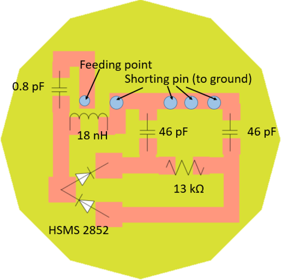
Figure 7. Rectifying system pattern.
The values in Fig. 7 are already adjusted to this circuit pattern and components' availability in order to achieve the maximum conversion efficiency.
Numerical results
In this section, numerical results that are based on ADS simulations are presented. Figure 8 shows the rectifying efficiency and output voltage (at load) for different input power levels. The rectifying efficiency is the ratio between the power consumed by the load and the power provided by the power source. Because of reflection, the power provided by the source is slightly higher than the power consumed by the whole circuit.

Figure 8. Efficiency and output voltage results for different input power (rectifying efficiency = 41.22%, output voltage = 0.354 V with −16 dBm input power; rectifying efficiency = 31.15%, output voltage = 0.195 V with −20 dBm input power).
Due to the existence of the non-linear component, there is a phase delay between the current and the voltage. Thus, the input power is calculated by:
 $$P_{active} = \hbox{Re}[U_{rms} \times \hbox{conj} (I_{rms})] $$
where Urms and Irms are the voltage and the current in the phasor form with the amplitude as root mean square (rms) values right after the receiving antenna respectively.
From the results shown in Fig. 8, it appears that when the source provides a total power of −20 dBm, the rectifying efficiency is 31.15%, and the output voltage could achieve 0.195 V. Comparing with the work in [Reference Bakogianni and Koulouridis21], the rectifying efficiency at −16 dBm is 41.2% which is 10% better.
As the value of the load depends on different applications, it is also interesting to find the impact of load on the rectifying efficiency and output voltage. Figure 9 shows different efficiencies and output voltages as a function of different loads with a power input of −20 dBm.

Figure 9. Efficiency and output voltage for different load resistances (rectifying efficiency = 31.17%, output voltage = 0.19 V with 13 kΩ load resistance).
As seen, the rectifying efficiency reaches a local peak value when load is 13 KΩ. As the load increases, the power at the load decreases but the output voltage increases continuously, which might be used as a voltage trigger.
Matching circuit comparison
There are many possibilities for the number of components in a matching circuit. In this section, a three-component matching circuit is presented at the aim of comparing with the two-component design and proves the superiority of the two-component design against other multiple component designs. The circuit is shown in Fig. 10.
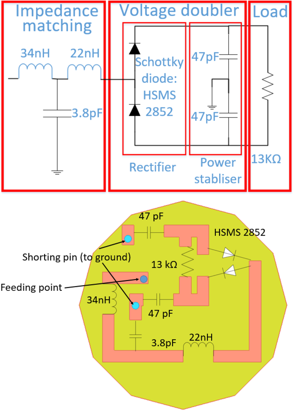
Figure 10. Three-component rectifying system design.
In this design, the rectifying circuit consists of three different elements. Apart from this difference, the total lengths of transmission lines are even shorter than the previous design. However, the total efficiency is 23% at a power input of −20 dBm (shown in Fig. 11), which is less efficient than the previous two-component design.

Figure 11. Efficiency and output voltage results for three-component design (rectifying efficiency = 22.976%, output voltage = 0.168 V with −20 dBm input power).
Diodes comparison
Apart from matching circuits, the choice of diodes is also important. Skyworks 7630 and HSMS 2850 are both frequently used for low power rectifying. In this section, the performance of these two diodes are examined and compared in the same circuit pattern. The efficiency and output voltage are the main criteria for this comparison.
The ADS model of diode Skyworks 7630 is not provided by the Skyworks company. In this paper, a Spice model together with the SOT-23 package model [22] is used as a realistic model for ADS simulation. Figure 12 shows the rectifying efficiency and output voltage results for Skyworks 7630 diodes with different input power levels.

Figure 12. Topology and rectifying results for Skyworks 7630 diode (rectifying efficiency = 35.16%, output voltage = 0.183 V with −20 dBm input power).
Compared to the results in “Numerical results”, the rectifying efficiency for this diode is 4% better than the previous model. However, this model is less accurate because it is created from the Spice parameters and SOT-23 package model. In contrast, HSMS 2850 exists already in the ADS library and is thus more trustworthy. In conclusion, although there is a tiny difference of the rectifying efficiency between the two diodes, the HSMS 2850 diode is chosen for this rectifying circuit.
Experimental results
Antenna test
During the experimental validation, minced pork is used for simulating human tissue and is put inside a plastic cup. The thickness of the cup is negligible. However, due to the fat component and air bubbles between the pork and cup, the dielectric constant of the simulated “human tissue” is smaller than normal muscle. Furthermore, there exists another layer of glue below the superstrate since it is glued to the patch. Thus, some slight adjustments should be done to the antenna design before the fabrication.
The embedded antenna is fabricated, soldered together with the coaxial cable, then stick with superstrate by glue. A network analyzer is used to measure the reflection coefficient of the antenna. The fabricated antenna is shown in Fig. 13.

Figure 13. (a) Fabricated antenna comparing with one euro cent, (b) complete antenna with coaxial cable and superstrate and (c) antenna embedded into minced pork.
Unlike the ideal simulation environment, the real case is more complicated and more difficult to control.
In the simulation, the metallic radiating patch has the same size as the substrate, which leads to a direct contact with the minced pork meat. Due to this contact, the resistance (the real part of the impedance) of the antenna at its first resonant frequency (403 MHz) is smaller and the reactance (the imaginary part of the impedance) of the second resonant frequency (915 MHz) is larger than without contact.
However, in the real case, some glue is used so as to stick the superstrate with the substrate. For the first measurement, since the edge of the metallic patch is thin, some glue covered it and hence isolate it from the surrounding minced pork meat, which avoided the contact mentioned before and thus made the resistance at 403 MHz higher and the reactance at 915 MHz lower. Therefore, the reflection coefficient at 403 MHz is around −6 dB instead of −20 dB (in simulation) and the second resonant frequency is at 1.04 GHz instead of 915 MHz (in simulation). The corresponding measurement results are shown in Fig. 14(a). Because the results are different from those of the previous simulations, another simulation in which the metallic patch is surrounding by 0.3 mm of glue was done, the results are also shown in the same figure, which matches well the measurement result. This simulation model is presented in Fig. 14(b).

Figure 14. (a) First measurement results and corresponding simulation when patch is isolated by glue and (b) corresponding simulation model.
Meanwhile, in order to confirm the results from the design in previous chapters, a second measurement is done with the surrounding glue cut away from the antenna (patch exposed to pork meat). Figure 15(a) shows the comparison of the measurement and simulation results. There is still slight difference which is probably caused by air bubbles in the minced pork. The experimental results match globally the simulation results.

Figure 15. (a) Second measurement results and corresponding simulation when patch is expose to the minced pork meat and (b) corresponding experimental model.
Circuit test
As an essential part of the power transmission system, the circuit is tested separately in order to measure its performance. Figure 16 shows the unsoldered and soldered circuit. The circuit is fed by a coaxial cable from Pasternack company.

Figure 16. Soldered and unsoldered circuits.
The measurement is performed by the RHODES & SCHWARZ ZNB Vector Network Analyzer (VNA). The VNA provide −20 dBm of power from its output port for the circuit. The impedance of the total circuit and the voltage between the load are measured during the experiment. The load is an 18 kΩ resistance instead of a 13 kΩ but the results difference is negligible.
The total impedance of the circuit is around 32–31 jΩ, which is nearly matched with the standard 50 Ω impedance at 915 MHz. The reflection coefficient is −7.8 dB. The voltage at the load is measured as 0.07 V by a multimeter placed at the two ends of the 18 kΩ load. The value presents some difference with the simulation results, which is likely due to the tiny size of the circuit. The measurement impedance could even be affected by the different size of soldering dot. Some more advanced experiments are still undergoing.
Sensors powering
Various micro-sensor grids for biomedical uses are studied and developed in recent years. These sensors cost low power and have small sizes to be suitable for implanting uses. In Table 4, several sensors together with its feeding power, supply voltage, area of circuit, and effective number of bits (ENOB) are presented.
Table 4. Low cost sensors and specific parameters

From the previous calculation, the power that a single power transmission system in this paper could receive for different transmission distances is shown in Table 5.
Table 5. Received power at difference distances

As seen, the sensors in the table require low energy and voltage to operate. They also occupy little space which is suitable for implanted uses together with the power transmission system in this paper. In order to match the two parts together, it is necessary to calculate the actual power that received by the load.
As shown in Table 5, the power transmission system is capable of feeding several sensors in terms of power. The mentioned results are calculated by simulations. These results are calculated by the power that received by the implanted antenna with the corresponding distance value and the rectifying efficiency & output voltage results with the corresponding power received. In both simulations, the port impedances are standardized to 50 Ω.
For the values in Table 5, the power at the input of the rectifying circuit is not always −20 dBm. This power varies with the change of transmission distances. However, due to the reference, the power emitted by the external antenna must not be higher than 30 dBm. Therefore, in all the results presented in Table 5, the power emitted by the external antenna is fixed at the maximum value of 30 dBm. When the external antenna is located 200 mm away from the human body, the implanted antenna can receive around 32 μW at load. This could support anyone of the sensors that mentioned in Table 4. However, a voltage booster is still needed for achieve the supply voltage of the sensors and will be tested in the future.
Conclusion
A miniature wireless power transmission system for biomedical uses is presented in this paper. A complete scenario from external antenna to sensor powering is detailed and discussed. This power transmission system operates at 915 MHz. Several simulations are done for both the antenna and the rectifying circuit part. A comparison of the numerical predictions with experimental measurements proved the validity of the global system. The dual-band embedded antenna could receive around 77 μW from an external patch antenna at a distance of 200 mm and then 44.5% of it could be converted into DC power, which is around 32 μW in total. At a 400 mm distance, the received DC power decreases to 4.33 μW. In addition, it is also tested that the circuit is capable of rectifying AC into DC power with an optimum efficiency. Some experimental results are obtained and more accurate results are under procedure. In the last section, it is proved that this system could support the feeding of several kinds of sensors in terms of received power.
For the future work, several single systems could be combined together and operate at the same time in order to increase the output voltage and rectifying power. An external signal enhancing solution could also be possible.
 Shuoliang Ding was born in Shenyang, China in 1994. He received both his diploma engineer degree from the Ecole Centrale de Nantes in France and diploma master degree from Beihang University in Beijing, China in 2017. He is currently pursuing the Ph.D degree in CentraleSupelec in Paris, France. In 2017, he joined the Group of Electrical Engineering in Paris (GeePs). During his Ph.D study, he has authored several papers in international conferences. His current research interests include bio-electromagnetics, antenna theory, implantable antenna design, and wireless powering devices for biomedical applications.
 Stavros Koulouridis was born in 1975, in Athens, Greece. He received the Diploma Engineer in Electrical and Computer Engineering and the Ph.D. degrees in Microwave engineering from National Technical University of Athens, Greece, in 1999 and 2003, respectively. From 1999 to 2003 he worked as Research Engineer in Microwave and Fiber Optics Lab and Biomedical Simulations and Imaging Unit, National Technical University of Athens. He taught several classes in the School of Pedagogic and Technological Education (ASPAITE) from 2000 to 2003. He was also teaching assistant from 2000 to 2002 in National Technical University of Athens. From 2004 to 2008, he worked as Postdoctoral Researcher at the Electroscience Laboratory, The Ohio State University, Columbus, OH, USA. In March 2009 he joined Electrical and Computer Engineering Department, University of Patras, Greece and since August 2013 he holds an Assistant Professor position. From 2015 to 2016 he was visiting professor in Group of electrical engineering – Paris (GeePs) / CNRS-CentraleSupelec – Univ. Paris-Sud – Université Paris-Saclay - Sorbonne Université. He leads the Microwave Communications group. His research interests include Antenna and Microwave Devices Design, Development and Fabrication of Novel Materials, Microwave Applications in Medicine, Electromagnetic Optimization Techniques, Applied Computational Electromagnetics. He was the recipient of a three year PhD Scholarship on Biomedical Engineering from Hellenic State Scholarships Foundation in 2001. In May 2005 he received the annual award for the best dissertation in National Technical University of Athens. He is the Chair of IEEE AP/MTT/ED Local Greek Chapter. He was the General Chair of IWAT 2017 (International Workshop in Antennas Technology). He has published over 80 refereed journals and conference proceeding papers. He is serving as reviewer for several scientific international journals.
 Lionel Pichon received the Dip. Eng. from Ecole Supérieure d'Ingénieurs en Electronique et Electrotechnique in 1984. In 1985 he joined the Laboratoire de Génie Electrique de Paris where he earned a PhD in electrical engineering in 1989. He got a position at the CNRS (Centre National de la Recherche Scientifique) in 1989. He is now Directeur de Recherche (Senior Research Scientist) in GeePs (Group of electrical engineering – Paris), a laboratory belonging to four institutions: CNRS, CentraleSupélec, Université Paris-Saclay, Sorbonne Université. His research interests include computational electromagnetics for wave propagation, scattering and electromagnetic compatibility.


 Open access