

I. INTRODUCTION
Wireless power transfer is an old topic [Reference Tesla1] of much current interest [Reference Kurs, Karalis, Moffatt, Joannopoulos, Fisher and Soljavcić2, Reference van Wageningen and Staring3] with significant competition between standards and approaches. Most approaches utilize magnetic induction to carry power from a transmitting coil to one or more receiving units. Operation frequencies between 100 kHz and tens of MHz have been considered with the license-free ISM bands at 6.78 and 13.56 MHz being attractive choices. Metamaterials have been demonstrated to usefully contribute to these systems by helping to concentrate magnetic flux on its way from transmitter to receiver [Reference Urzhumov and Smith4] and have also been considered as power delivery media [Reference Stevens5, Reference Wang, Yerazunis and Teo6]. Following the original work on two terminal systems [Reference Kurs, Karalis, Moffatt, Joannopoulos, Fisher and Soljavcić2], where a power source drives a resonant transmitting antenna delivering power to a load via a single receiving coil, a number of researchers have considered approaches for increasing the range of efficient power transfer. Several methods have been employed to increase the range, notably the use of passive, resonant, relay coils to increase the oscillating magnetic flux at the receiving antenna. There are two main configurations for relays that have been studied – axial [Reference Lee, Zhong and Hui7] and planar [Reference Narusue, Kawahara and Asami8, Reference Mori, Lim, Iguchi, Ishida, Takamiya and Sakurai9]. Such relay coil arrays are identical to metamaterial structures.
In general, metamaterials are repeating arrays of resonant electromagnetic elements and in this work we are concerned with magnetically active varieties [Reference Stevens, Chan, Stamatis and Edwards10]. Periodic arrays of coupled circuits such as those employed in metamaterials generally support several modes of signal propagation. In 2002, magnetic metamaterials were discovered to exhibit a novel type of wave propagation known as a magneto-inductive wave (MIW) [Reference Shamonina, Kalinin, Ringhofer and Solymar11] which may only propagate within its host metamaterial.
In the past work, MIWs have been considered as novel waveguides [Reference Shamonina, Kalinin, Ringhofer and Solymar12], for distributed data transfer systems [Reference Stevens, Chan, Stamatis and Edwards10, Reference Chan and Stevens13] and to carry signals in magnetic resonance imaging [Reference Wiltshire, Hajnal, Pendry, Edwards and Stevens14]. A significant advantage of this type of waves for power transfer is their strongly magnetic character which leads to efficient coupling to resonant electric circuits in their near field. By their very nature MIW with strong coupling offer low loss and wide bandwidth channels [Reference Stevens, Chan, Stamatis and Edwards10]. Thus a good power transfer structure is also perfectly prepared to offer a high-bandwidth communication channel with data capacity well above traditional near field coupled (NFC) systems.
This paper deals with the application of MIW to power transfer via a one-dimensional (1D) structure which supports them. When driven by a suitable source and coupled to a power receiver MIW carry energy from source to load wherever it is placed on along the device. As an example, such a device could be used to recharge a number of mobile telephones equipped with contactless power receivers. A simple scheme for this is shown in Fig. 1 along with its equivalent circuit and it is this scheme that we consider for the rest of the paper.

Fig. 1. Simple structure for a MIW-based near-field power transfer structure using a MIW line. Equivalent circuit showing the first neighbor coupling and receiver coupling terms.
Section II details the modeling of MIW power transfer lines and is divided into three parts.
Section IIA describes the properties of MIWs , the benefits they convey in terms of bandwidth and offers a simple figure of merit for structure design.
Section IIB uses MIW characteristic impedance to determine the input impedances for semi-infinite MIW-based power transfer structures for two different source connections.
Section IIC considers finite length structures and the impact of standing waves on input impedances, finally calculating power transfer efficiency for a model line under three different constraints.
Section III reports results of a simple experiment on one such finite line and compares the performance with predicted values.
Section IV considers future approaches to further optimizing the structure in light of the results with potential for power transfer efficiency in excess of 80% to loads at a range of 800 mm along a MIW line from the driving source.
II. MIWs AND POWER TRANSFER
Metamaterials for resonant frequencies are generally formed using periodic arrays of resonant circuits (“cells”). Magnetic metamaterials (being those designed to exhibit a strong magnetic permeability) utilize simple series resonant circuits (inductance L, resistance R, and capacitance C), which are often coupled together via the mutual inductance between adjacent cells. Figure 1 shows a typical, 1D metamaterial structure, whose cells are square tracks with series capacitors bridging a small gap in the conductors forming the LC resonator. The cells are very close to one another so that a current circulating in one cell generates a significant magnetic flux through the neighboring cells and hence they are coupled via a mutual inductance M. If a resonant current is induced in one cell, the mutual inductance results in a current being stimulated in the cells neighbors. These in turn stimulate their neighbors and this is the propagation of a MIW [Reference Shamonina, Kalinin, Ringhofer and Solymar11]. A key feature of these structures is that they are open: the magnetic flux linking the cells extends beyond the structure and provides a region of near field from which nearby structures can draw power or data signals. The power transfer device which is the subject of this paper is formed by connecting an radio frequency (RF) source directly to one of the cells of a conventional MIW guide as shown in the lower pane of Fig. 1. Power is then delivered to one or more receivers in the near field of the guide.
A) MIWs
Detailed descriptions of the properties of MIWs can be found in the literature [Reference Stevens, Chan, Stamatis and Edwards10, Reference Shamonina, Kalinin, Ringhofer and Solymar11–Reference Solymar15] and need not be repeated here. We include the key results below. In general, there is a limited bandwidth available for signal transmission via this type of channel with the bandwidth increasing as the mutual inductance coupling rises while the losses commensurately decrease. In consequence the optimal structure for both power and high-bit-rate data transfer requires that the mutual inductive coupling between cells be as high as possible. This coupling is usually characterized by the parameter k = 2M/L, where M is the nearest-neighbor mutual inductance and L is the self-inductance of each cell.
MIWs are described in terms of the currents circulating in each cell (In for the nth cell) and the general expression for a MIW in 1D is I = I 0 e (a + jb)nd , where a is the attenuation and b is the wave vector, and d is the period of the cells. Attenuation at the cells resonant frequency is then given by equation (1) where αd is the attenuation per cell for MIW transmission (in a structure with a period of d) and Q is the individual cell's resonant quality factor measured in isolation [Reference Hao, Stevens and Edwards16].
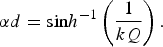 $$\alpha d = {\rm sin}h^{ - 1} \left( {\displaystyle{1 \over {kQ}}} \right).$$
Its very clear that for efficient power transmission in this medium strong coupling (high k) and low loss (high Q) resonators are preferred. Hence in optimizing metamaterial power transfer designs, care should be taken that the figure of merit kQ = 2ω 0 M/R be as high as possible. Propagation for waves in such a very low loss system is then governed by a simple dispersion equation.
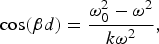 $${\rm cos}(\beta d) = \displaystyle{{\omega _0^2 - \omega ^2} \over {k\omega ^2}},$$
where, ω
0 is the cell resonant angular frequency
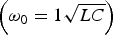 $\left( {\omega _0 = 1\sqrt {LC}} \right)$
. The band limits for MIW transmission are then defined by the frequencies for which |cos(bd)| = 1. This provides a simple expression for the bandwidth which is shown in equation (3)
$\left( {\omega _0 = 1\sqrt {LC}} \right)$
. The band limits for MIW transmission are then defined by the frequencies for which |cos(bd)| = 1. This provides a simple expression for the bandwidth which is shown in equation (3)
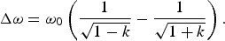 $$\Delta \omega = \omega _0 \left( {\displaystyle{1 \over {\sqrt {1 - k}}} - \displaystyle{1 \over {\sqrt {1 + k}}}} \right).$$
In a 1D structure with |k| = 0.3 the bandwidth available for MIW transmission will be 31% of the cell resonance frequency ω 0 [Reference Shamonina, Kalinin, Ringhofer and Solymar11] given by setting k = 0.3 in equation (3).
B) Input impedance and matching
For a 1D MIW there is a simple matching condition [Reference Solymar15] when only first-order coupling is significant which states that a structure is perfectly terminated if the last cell in a line includes an extra impedance Z m given by
 $$Z_m = j\omega Me^{ - (\alpha \,+\, j\beta )d}.$$
In practice, this is a rather difficult situation to achieve as the value of Z m is a complex frequency dependent function and only has a pure real value (i.e., resistive character) at ω 0. Despite this, in terms of determining the match between a source and a MIW line or a load coupled to one Z m allows a simple analysis to be performed.
We have investigated two configurations of source connection directly to one cell of a MIW line, in series with the components of that cell or in parallel across the capacitance of the cell.
We consider two locations for a source directly coupled to the MIW line. First a source coupled to the first or last cell of a line (END). Second, a source coupled to a cell in the middle of the line (MID). Equivalent circuits for the two cases are shown in Fig. 2.

Fig. 2. The two cases for parallel power connection to the MIW line showing the use of the matching impedance Z m to allow calculation for an infinite line.
In the END case the first cell of the line, to which the source of internal resistance R s is coupled (in parallel with the resonating capacitor or series with the cell) includes an element of impedance Z m . This is sufficient to model the source being connected to the start of a semi-infinite line. For the MID case the driven cell is linked to two semi-infinite lines and so is modeled with two identical impedances Z m for the MIW launched by this source along the two directions of the infinite line. Using these two simplifications the matching condition for any driving frequency can be obtained. Using simple circuit methods the effective input impedances (Z in = R in + jX in ) presented to the source in each case can be derived for these parallel configurations (source connected across input cell's capacitor) as
 $$\eqalign{\displaystyle{1 \over {Z_{in}}} = &\; j\omega C + \displaystyle{1 \over {R + j\omega L + Z_t}} \quad Parallel, \cr Z_{in} = &\, R + j\left( {\omega L - \displaystyle{1 \over {\omega C}}} \right) + Z_t \quad Series,}$$
where Z t is given by Z m for the END case and 2Z m for the MID case.
Figure 3 shows the results for the two configurations (parallel and series) for both locations (END and MID). Values used in this calculation were derived from FastHenry [Reference Kamon, Tsuk and White17] simulations of w = 1 mm wide tracks forming square single turn inductors with side length of a = 40 mm, separated by gaps of g = 0.2 mm. Cell resistance is taken to be 88 mΩ from the copper conductor losses. Within the pass-band there is a significant difference between the two impedances and their frequency dependence.

Fig. 3. Input impedances for sources connected in the two locations (END and MID) in both parallel and series configuration. Resonant frequency of 13.6 MHz is indicated. Cell parameters in this case are L = 130 nH, C = 1.05 nF, R=88 mΩ, M1 = −16.5 nH, and |kQ|=32.
The parallel END case input impedance has a maximum real component near the center of the band falling to near zero at the band edges, while its imaginary component peaks at the lower band edge, falls to zero at the resonant frequency f 0 and then goes negative with a negative peak near the top of the band.
The parallel MID case exhibits a real input impedance that is peaked near the band edges and has a minimum within the pass-band above the resonant frequency. For the majority of the pass-band the real value only varies by ±15% about 46.3 Ω for 65% of the bandwidth. The imaginary component of the parallel MID input impedance has a nearly frequency independent value for most of the pass-band which is negative (with a value of −11.7 Ω for these parameters).
The series connections both exhibit a much smaller impedance than the parallel version. Both real components are smoothly peaked near to the resonant frequency of 13.6 MHz with the MID case having nearly twice the real resistance as the END. Most attractive is that the imaginary part of the MID input impedance is very close to zero for the whole passband (−0.2<X MID <0.2).
Conventionally the maximum power transfer theorem suggests that maximum power is provided from a source to a load when both have the same impedance. In such a case the efficiency is only 50% as half the power generated by the source is lost internally. Hence for high-efficiency power transfer, it is preferable to mismatch the source and load with the source impedance being as low possible. Thus, in order to maximize the power transfer efficiency for this system the parallel connection is preferred as this presents a much higher input impedance than the series variant. Power transfer only requires that a single frequency be transmitted but this introduces problems when reflections from the ends of finite lines are considered. Standing waves resulting from such reflections will modulate the smooth curves for impedance and reflection.
C) Finite lines
As alluded to at the end of Section IIB real lines will be finite so that standing waves are expected to impact the performance for most applications unless the line ends are terminated. In a power transfer system absorbing terminations for the MIW are quite undesirable as they will lead to large fixed losses and seriously degrade overall efficiency unless they are themselves the loads to which power is being provided. Hence, we confine ourselves to considering unterminated lines where the only losses are those intrinsic to the line (the resonator loss R), the source loss R s and one or more loads inductively coupled to the line. To perform finite line calculations we adopt the circuit modeling approach as has been employed previously [Reference Stevens, Chan, Stamatis and Edwards10] to compute currents in each cell of a line and each receiver coupled to it. In brief this method uses the impedance matrix (Z) for the set of coupled cells and receiver which is numerically inverted for each frequency under consideration and then used to determine the currents i circulating in the cells of the device driven by the source(s) (V).
 $$\eqalign{& {\bf V} = {\bf Zi} \cr & {\bf i} = {\bf Z}^{ - 1} {\bf V}}$$
Circuit modeling uses the matrix inversion method described elsewhere [Reference Solymar15] and in this case we include coupling terms to third-order (1st, 2nd, and 3rd neighbor mutual inductances: M 1, M 2, and M 3, repectively), are included for the cells forming the lines and for the receiver elements. To compute the input impedance the current drawn from a source is calculated for each frequency and compared with the potential generated across the input of the MIW. Output power is computed by adding a load to the receiver element which is otherwise identical to those forming the line. Loads are connected to a receiver inductively coupled to the five cells closest to it. The load impedance may be either series connected with the LRC elements of the receiver resonator, or in parallel across its capacitance, as shown in the two receivers of Fig. 1.
1) Input impedance and standing waves
Figure 4 (left pane) shows the input impedance calculated for a finite 21 cell line excited either at its first cell (END parallel) or at cell number 11 (MID parallel) compared with the infinite line calculations from Fig. 3. Cell parameters are the same as those used previously with extra values computed using FastHenry [Reference Kamon, Tsuk and White17] for the second and third nearest-neighbor couplings. To obtain these results the receiver is effectively removed by setting its coupling inductances to zero. In all source cases, the effects of standing waves are to modulate the input impedance components about the infinite model result. The amplitude of the standing waves is clearly greater for the MID case as would be expected (waves only have to travel half as far to the reflective ends of the structure for the MID as compared with END case). In general, for high-power transfer efficiency one would like to minimize the cell resistance in order to ensure cell losses are as insignificant as possible. The results of Fig. 4 (left) show that this would offer a penalty in terms of the standing waves influence.

Fig. 4. (Left) parallel coupled input impedance for MIW line 21 cells long computed at the center (MID) and the ends (END) without a receiver and load. (Right) the same calculation but with a load present and strongly coupled to an end cell. Lines are infinite model calculations from Fig. 3. Circuit parameters are identical to those used for infinite model with M2 = −0.60 nH and M3 = −0.96 nH. Receiver coupling is 57.0 nH to the end cell and −8.3 nH to the next nearest.
The right pane of Fig. 4 shows the results for the input impedances when a load is coupled to the end of line (opposite to the end used for the END case). This receiver has a load of 5 Ω connected in series with its LRC components and is strongly coupled to the line (set at a distance of 3 mm above for FastHenry [Reference Kamon, Tsuk and White17] calculations). The modulation depth of the standing waves is significantly reduced in this case as 70% of the power arriving at this end is now being absorbed by the load.
Two conclusions can be drawn from this result. Firstly, standing waves are not a serious impediment to power transfer as, when one has a well-coupled load they are suppressed removing the strong frequency variation in input impedance that they generate for the unloaded line. Secondly, the infinite model input impedances are in fact quite close to those for the finite case when the load is strongly coupled making these results useful in determining optimal source and receiver parameters.
2) Power transfer efficiency
With a single receiver located above one of the cells of the line, power is sent to that receiver's load by the source driving the line. Power efficiency is calculated including the source losses in R
s
using circuit modeling and matrix inversion as described elsewhere [Reference Stevens, Chan, Stamatis and Edwards10] to find the currents in each cell plus the receiver, then using them to obtain power at the load (P
LOAD
= |i
R
|2
R
L
), while power from the source is evaluated as the real part of the complex product of source voltage and current
 $(P_{input} = \Re (V_S i_{input}^* ))$
. The maximum voltage (V
B
) that may be applied to a line is limited by the breakdown potential of the capacitor used to set the cell's resonant frequency.
$(P_{input} = \Re (V_S i_{input}^* ))$
. The maximum voltage (V
B
) that may be applied to a line is limited by the breakdown potential of the capacitor used to set the cell's resonant frequency.
Figure 5 shows the results of one such calculation for a line, consisting of 21 cells and 1 receiver. Each cell is the same as those used for the impedance calculations previously and all parameters are the same. A low impedance source of 1 Ω is connected in parallel to the central cell (the 11th in the line) and the load resistance and receiver height allowed to vary. The load is connected in series with a receiver cell located at a height z (1–20 mm) above each of the cells of the line in turn. The receiver here is identical to the cells of the line which are the same a = 40 mm square loops as introduced earlier.

Fig. 5. Predicted performance parameters [efficiency (a), output power (b), operating frequency (c), load resistance and receiver height (d)] for a 21 cell line driven by a source connected to its central cell. Three cases are shown for properties if driven at a fixed frequency of 13.6 MHz, at the frequency giving maximum efficiency (f 0 pt) and at that frequency that generates maximum output power.
Three cases are considered here. Firstly driving the source at a fixed frequency (13.6 MHz) and then seeking the combination of R L and height z that give the largest efficiency. For this case we show the power output under these conditions along with the load resistance and the height that give the maximum efficiency. The second and third cases are obtained by allowing the drive frequency to vary over the entire MIW band and finding the combination of R L , z, f that give maximum efficiency (‘opt’ case) and maximum output power (‘maxP’ case)
Efficiency: Figure 5(a). Fixed frequency efficiency (η13.6) peaks at 77% in the degenerate case (receiver directly above the source at cell 11) to 1.9% for the 2nd and 20th cell locations. The even numbered receiver locations have much lower efficiency and power than the odd numbered positions. The origin of these oscillations is the generation of standing waves between the source and the cell coupled to the load from which waves are reflected. The resonant frequency has a wavelength of exactly four cells resulting in standing wave peaks every 2 cells. Turning to the maximum efficiency (ηopt) one finds a higher degenerate peak of 93% and the lowest value at the ends of the line of 38%. The peak arises in the region where the direct coupling between source and receiver adds to the power transferred via MIW to enhance the efficiency. At a distance of two cells the direct coupling becomes insignificant and all power is being delivered via the MIW line. Maximum output power efficiency (η maxP ) is only 51% and drops to 24% at the ends of the line. It is notable that the maximum efficiency coincides with that for the fixed resonant frequency drive of 13.6 MHz for the odd numbered cells where standing wave peaks are generated.
Output power: Looking at the output power (Fig. 5(b)), values for the fixed frequency vary between 3.5 W and 13 mW due to the standing wave interference, while the maximum efficiency and maximum power cases result in more consistent performance. The maximum efficiency case gives output powers ranging from 2.4 W (x r = 11) to 0.6 W at the ends. The majority of the degradation in both output power and efficiency arises from the attenuation of the MIW over the ten cells between source and the ends of the lines. Maximum output power peaks at 17.7 W dropping to 0.93 W at the ends. Once again the maximum efficiency, maximum output power cases and peak 13.6 MHz values tend to converge away from the source cell.
Frequency: The frequencies corresponding to the three cases are shown in Fig. 5(c). Away from the central source cell these are close to, but generally above the resonance frequency varying between 13.6 and 15.5 MHz.
Load Resistance and height: Finally the optimal load resistances and receiver heights have been evaluated as shown in Fig. 5(d). Standing waves near the line ends result in large variation in these parameters but away from them the optimum load resistances lie between 1.5 and 4 Ω, while the optimal height is close to 7 mm. It is useful, at this point, to make some observations based on the above data. Firstly at least for this type of capacitor loaded resonator, the overall length in cells should be short to minimize attenuation losses. If a fixed drive frequency is required (as is likely given the licensing restrictions on RF systems), then the resonant frequency for the cells of the line should be chosen lower than the drive frequency for best performance. For best performance the drive frequency should be allowed to vary between 13.6 and 15 MHz. In fact, it is possible that only two drive frequencies (13.6 and 14.5 MHz) would be required to give near optimal performance at all cells.
III. EXPERIMENTAL VERIFICATION
To confirm the predictions of the circuit-based modeling described in the previous section a simple experimental verification has been conducted. The 21 cell line made from a = 40 mm cells spaced g = 0.2 mm apart would be nearly 850 mm long and was impractical to fabricate for a test of this kind. We instead constructed a smaller five cell line whose total length is 201 mm. Tracks were laid out w = 1 mm wide and fabricated by PWCircuits Ltd. [18] on an FR4 substrate using photo-lithography. Each cell was a square single turn loop and had a maximum outer dimension of 40 × 40 mm with a 0.2 mm gap between cells. Surface mount ceramic multilayer capacitors (1 nF 603 size, C0 G dielectric Kemet Ltd.) were soldered across gaps in the tracks to form a resonator. The power receiver is a resonator of identical dimensions to the MIW cells but has an extra gap across which the series load of 3.3 Ω is connected.
Initially measurements of individual resonators loaded with 1 nF capacitors gave a resonant frequency of 13.75 MHz with a Q factor of 37. Hence, the real inductance of the individual resonators was 134 nH. Using a pair of cells the effective first-order coupling between them was determined from the split of their resonances giving a value for M1 of −16.33 nH, very close to the predicted values of L = 130 nH and M1 = −16.5 nH from FastHenry [Reference Kamon, Tsuk and White17]. The Q factor implies a cell equivalent resistance of 307 mΩ which is rather higher than the 88 mΩ copper loss value used in the simulations reflecting the significant extra losses from solder (typically 100 mΩ per joint), the ceramic capacitors equivalent series resistance (11 mW from the manufacturers datasheets) and possibly some radiation loss. This larger resistances inevitably increase the losses associated with MIW propagation for this system but as we are only using five cells it should be tolerable. The figure of merit for this structure |kQ| = 9.1 in contrast to the figure of 32 expected for the copper loss alone.
The experimental apparatus is shown in Fig. 6. Measurements were made using a vector network analyser (VNA) to provide the source (connecting directly across the central cell's capacitor) and to measure the received signals connecting across the load resistance. Care must be taken when analysing data using the VNA (Z 0 = 50 Ω) to adjust for the difference between the VNA impedance and the actual load resistance. In order to convert the measured forward scattering parameters to power transfer efficiency ( = power to load/power into line) one must combine the forward and reverse scattering parameters to find the effective efficiency from a simple source as shown in equation (7).
 $$\eta _{power} = \displaystyle{{S_{21}^2 (1 + Z_0 /R_L )} \over {1 - S_{11}^2}},$$
where Z 0 is the characteristic input impedance of the VNA (50 ΩW) and R L is the load resistance across which the output is measured. Hence for this 3.3 Ω load the power efficiency is more than 16.1 times the measured value for the forward scattering parameter. This efficiency does not however include any source losses as the data has effectively been corrected for them by this process. To compare with a model calculation one must set the source impedance to a very low value. In a realistic implementation of course, there will be some source losses which reduce the overall system efficiency below these values.

Fig. 6. Experimental apparatus for measurements of power transfer.
The receiver is swept along the line in 5 mm steps for heights above the line in 1 mm increments with the closest approach between the copper layers of the line and receiver being 1.6 mm. Maximum separation between line and receiver was 26.6 mm. Two source connections were evaluated – one in the MID position (cell 3) and one at the END location (cell 1). Both cases were modeled using the same circuit method previously described for comparison with |kQ| = 9.1 as determined from the discrete resonator performance. Figure 7 shows the peak efficiency for each longitudinal position of the receiver along with the frequency for this maximum performance for the two source configurations. We also plot discrete points for the computed model power transfer efficiency corresponding to the five locations where the receiver is aligned to one of the MIW cells. Maximum efficiency in both cases occurs when the receiver is aligned (location TX in the figure) with the transmitter and is 75% for both END and MID cases. This drops quickly and by the time the receiver is two cells away from the source the efficiency has dropped to around 45%. The rapid drop here is attributable to a combination of the rapid falloff of the direct coupling between source cell and receiver adding to the MIWs’ attenuation. After this the dominant power transfer mechanism is via MIWs. The frequencies at which these maximal efficiencies are obtained are also shown. There are large variations in the optimal frequency near the transmitter but these converge to a value just above the resonant frequency away from the source. The calculated power transfer efficiency matches most of the locations quite well but the TX point generally has a higher predicted efficiency than the measured value. Inspecting the height for which these maximum efficiencies are obtained at the TX point is always the minimum value of 1.6 mm. At this point some capacitive coupling between the TX cell and the receiver is to be expected which generally has opposite sign to the magnetic coupling for this configuration and hence acts to reduce the actual power transferred.

Fig. 7. (top left) Measured peak power transfer efficiency for a line with source driving one end (crosses) compared with predicted values for receiver aligned with each cell in turn (circles). Here the calculations are made with a cell resistance of 0.3 Ω matching the experimental values derived from measured Q factors. (bottom left) Optimum frequency for maximum efficiency with END drive. (top right) Peak efficiency for MID drive. (bottom right) Optimum frequency for this case.
At more than two cells horizontal displacement from TX MIW dominate the power transfer and the strong MIW attenuation present in our test structure becomes the main limitation on overall efficiency.
IV. DESIGN METHODOLOGY AND OPTIMIZATION
By understanding the MIW properties of the line one may rapidly find the potential performance of any relay coil/MIW device. For a series connected source, driving one end of a semi-infinite line, the input impedance at resonance is very close to ω 0 M and approximately double to this for mid-line sources. This is also true for finite lines, when they are well terminated by an absorbing load (possibly that to which power is being supplied). Attenuation on the line is given by equation (1) and longer the line the greater the loss for power transfer to the ends given by 1−e −αd . In order to perfectly match the line the load must introduce an effective impedance to the line equal to the series input impedance. This in turn determines the height or a receiver terminal and its load. These design rules can be expressed in the simple form of equation (8), where n D is 1 for a semi-infinite line and 2 for an infinite case and the approximation on attenuation holds well for kQ > 5. The expressions assume perfect termination at the resonant frequency by a load whose impedance is equal to the input impedance.
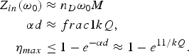 $$\eqalign{{Z_{in}}({\omega _0}) & \approx {n_D}{\omega _0}M \cr \alpha d & \approx frac1kQ, \cr {\eta _{max}} & \le 1 - {e^{ - \alpha d}} \approx 1 - {e^{11/kQ}}.}$$
It is clear from the rather low values of the experimental efficiency that the higher than anticipated effective cell resistance and reduction of the figure of merit to 9.1 from 32 has resulted in too much loss. Future design for metamaterial power transfer could counter this by several strategies:
Multiple turn inductors: As the product kQ controls the magnitude of attenuation for MIW increasing Q by raising the resonator inductance seems an obvious choice. In isolation L may be increased by a very large factor using spiral structures with increasing numbers of turns. While this raises the resistance linearly it raises L in a super linear fashion so that their ratio controlling Q(= ωL/R) can be significantly enhanced. If one is winding coils on cylindrical cores this is very effective but leads to a rather thick and complex structure in terms of manufacturing. Q factors as high as 800 have been reported for such coils [Reference Breitkreutz and Henke19]. For planar PCB inductors multiple turns can be achieved using spiral patterns but care must be taken as, should the inner dimension of the spiral become too small, the value of k will decrease. Using the wheeler method for square coils, a three turn spiral with 1 mm track widths and inter track gaps of 0.2 mm made from 35 μm thick copper would offer Q in excess of 180 but will reduce k to −0.20 giving |kQ| = 36.
Self-resonant structures: In our test structure the resonators’ resonances were set to 13.56 MHz by adding a low loss surface mount capacitor to each cell. This added series resistance and degraded the overall Q factor. Using resonator structures that do not require this lumped element offers potential for very much higher Q values and longer range power transfer structures. Planar spirals, broadside coupled split rings, multi-layer spirals [Reference Hao, Stevens and Edwards16], and others all offer higher Q possibilities but are difficult to design for frequencies as low as 13.6 MHz. Wound self-resonant coils can offer Q factors in excess of 1400 but present manufacturing penalties [Reference Breitkreutz and Henke19].
Enhanced coupling: Our test structure is a purely single-layer planar design but this imposes strong limitations on the maximum possible coupling and the value we achieve of k = −0.24 is close to the realistic limit for symmetric cells of this type. The coupling can however be much larger if structures use more than one later and the cells of each layer are overlapped [Reference Radkovskaya, Sydoruk, Shamonin, Stevens, Faulkner, Edwards, Shamonina and Solymar20]. Alternately quasi-axial structures using cells each of which overlays the next by half its width also give good performance with coupling reported at k = 0.675 [Reference Syms, Solymar, Young and Floume21] although these have only been demonstrated using cells with very high aspect ratios (very long in the line direction). Using one or more of these approaches it is thus possible to significantly improve on the performance of our test structure. Using the circuit modeling method we have investigated how much efficiency could be improved as the kQ value increases. Literature values for magneto-inductive cables for instance [Reference Syms, Solymar, Young and Floume21], give Q of 48 and k = 0.675 to a total of 32. To explore the potential we calculate the power transfer to our single turn terminal for a variety of cell resistances and kQ values and the results are shown in Fig. 8.

Fig. 8. Predicted performance for a 21 cell line with |kQ| = 9.1, 32, 55, and 199. (left) Power transfer efficiency for an END connected source and (right) optimum frequency.
For a 21 cell line (844.2 mm long) our original cells (|kQ| = 9.1) would offer <4% power transfer efficiency end to end while cells with |kQ| = 32 could achieve in excess of 30% with better than 60% for lines of 400 mm or less. If one were to use the self resonant cells of reference [Reference Syms, Solymar, Young and Floume21] |kQ| = 55 is possible offering 50% for 21 cell lines. Using self-resonant coils taken from the literature [Reference Breitkreutz and Henke19] one may achieve |kQ| = 199 with 80% efficiency for the 21 cell line and better than 90% over 11 cells. It is important to note here that the frequencies for optimal power transfer shown for all these cases (Fig. 8 left) do not significantly vary as a function of the |kQ| value being only due to the effects of standing waves rather than any spectral variation of the attenuation within the passband. Hence optimization for power transport need only consider maximizing the |kQ| product.
V. CONCLUSIONS
This study has investigated the potential to transfer power efficiently between source and load via MIWs traveling on a 1D metamaterial waveguide. We have found that it is indeed possible to transfer useful power via MIWs with the breakdown of the resonating capacitors being the principal limitation. From this understanding of the nature of power flow along such a line we have developed simple methods to determine performance and obtain optimal design using very simple analytical formulae. Although experimental efficiency of only 40% was demonstrated potential exists for much higher performance if our resonators’ design can be improved. Power transfer is maximized when the product of the dimensionless coupling k (= 2L/M) and the cells resonant Q factor is maximized. Standing waves on low loss lines do not significantly limit power transfer but do result in a variation in the frequency for optimal efficiency. For 1D lines such as those explored here it is possible to obtain reasonable power transfer using two drive frequencies both of which are somewhat higher than the cell's resonance. Driving the MIW cells directly from a source is best achieved with a low impedance source connected in parallel and maximum power is extracted from the receiver if the load is placed as a series components in its resonator. The matching impedance in the experimental case was 3 Ω but use of cells with a larger mutual inductance would (as shown in equation (4)) offer a larger optimum load value. It is possible that better performance still could be obtained if the receiver were itself formed using a higher Q structure with more turns. Finally, it is useful to point out that MIW are present both in 1D and 2D structures offering the potential for power transfer surfaces covering relatively large areas if resonator design can be optimized. Such 2D structures exhibit larger bandwidths and lower loss than 1D waveguides but still offer the near field power and data coupling to simple receivers.
ACKNOWLEDGEMENTS
I gratefully acknowledge the support of Isis Innovations Limited in this work.
 Christopher J. Stevens read physics at the University of Oxford, UK, graduating in 1990 with first class honours and prizes for practical physics and received his D. Phil. degree in condensed matter physics in 1994 following a 3-year doctoral program at the same university. Subsequently he worked in Uiversita Degli Studidi Lecce after which he held a Royal Academy of Engineering fellowship at St. Hugh's College, Oxford. He now holds an engineering faculty position at the University of Oxford and is a Fellow of St. Hugh's College, Oxford. His current research activities include ultrawideband communications, metamaterials, ultrafast nanoelectronics, and high-speed electromagnetics.


