Hostname: page-component-788cddb947-pt5lt Total loading time: 0 Render date: 2024-10-19T02:35:02.088Z Has data issue: false hasContentIssue false

3D Nanoscale Imaging of Semiconductor Films for GAA (Gate All Around) Device Development

Published online by Cambridge University Press:  22 July 2022

Pritesh Parikh
Affiliation:
Eurofins Nanolab Technologies, 1708 McCarthy Blvd, Milpitas, CA, United States
Darshan Jaware
Affiliation:
Eurofins Nanolab Technologies, 1708 McCarthy Blvd, Milpitas, CA, United States
Jiangtao Zhu*
Affiliation:
Eurofins Nanolab Technologies, 1708 McCarthy Blvd, Milpitas, CA, United States
*
*Corresponding author: jiangtaozhu@eurofins-nanolab.com

Abstract

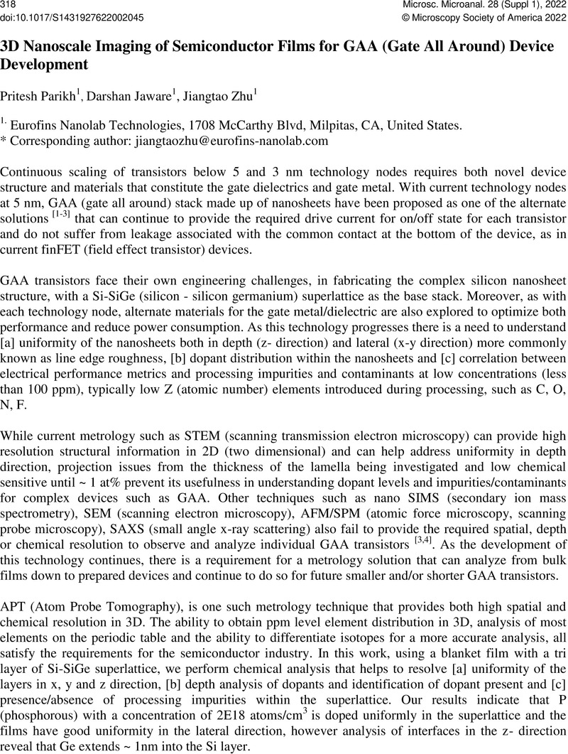
Image of the first page of this content. For PDF version, please use the ‘Save PDF’ preceeding this image.'
Type
Advanced 3D Imaging and Analysis Methods for New Opportunities in Material Science
Copyright
Copyright © Microscopy Society of America 2022

References

Nagy, D., Indalecio, G., GarcíA-Loureiro, A. J., Elmessary, M. A., Kalna, K. and Seoane, N., “FinFET Versus Gate-All-Around Nanowire FET: Performance, Scaling, and Variability,” in IEEE Journal of the Electron Devices Society, vol. 6, pp. 332-340, 2018, doi: 10.1109/JEDS.2018.2804383.CrossRefGoogle Scholar
Loubet, N. et al. , “Stacked nanosheet gate-all-around transistor to enable scaling beyond FinFET,” 2017 Symposium on VLSI Technology, 2017, pp. T230-T231, doi: 10.23919/VLSIT.2017.7998183.CrossRefGoogle Scholar
Das, U. K. and Bhattacharyya, T. K., “Opportunities in Device Scaling for 3-nm Node and Beyond: FinFET Versus GAA-FET Versus UFET,” in IEEE Transactions on Electron Devices, vol. 67, no. 6, pp. 2633-2638, June 2020, doi: 10.1109/TED.2020.2987139.CrossRefGoogle Scholar
Pott, V., Moselund, K. E., Bouvet, D., De Michielis, L. and Ionescu, A. M., “Fabrication and Characterization of Gate-All-Around Silicon Nanowires on Bulk Silicon,” in IEEE Transactions on Nanotechnology, vol. 7, no. 6, pp. 733-744, Nov. 2008, doi: 10.1109/TNANO.2008.2007215.CrossRefGoogle Scholar
Orji, N. G., et al. , Metrology for the next generation of semiconductor devices, Nature Electronics 1 (10), 532-547 (2018). https://doi.org/10.1038/s41928-018-0150-9CrossRefGoogle ScholarPubMed