


Introduction
Most modern devices contain components that leverage an interaction between light and electrons: displays, cameras, many sensors, photovoltaics and so on. A material that is transparent to visible light and also electrically conductive is often essential to these devices. Of the materials that fit these requirements, the most commonly used are transparent conducting oxides (TCOs), typically integrated into devices as thin films [Reference King and Veal1, Reference Li, Winget and Brédas2]. Because of its high transparency and conductivity, the most widely used TCO is indium tin oxide (ITO), where tin is the dopant [Reference Lin and Li3]. The relatively low natural abundance of indium drives up the financial and environmental cost of devices using this conductor [Reference Minami4]. Al-doped ZnO (AZO) is emerging as an earth-abundant replacement for ITO for applications that require transparent conductive n-doped thin films. Resistivity values as low as 10−3 Ω cm have been achieved for ZnO films, and doping can yield even lower resistivities [Reference Kim, Kang, Kim and Kim5]. Thin film deposition methods such as magnetron sputtering at moderate temperatures have been reported that match the relevant properties of ITO films [Reference Minami4]. AZO films have been deposited by many methods including chemical vapor deposition, sol–gel spin coating, aqueous synthesis, and magnetron sputtering, yielding a wide range of resistivities (10−2–10−4 Ω cm) [Reference Hu and Gordon6, Reference Chaitra, Muhammed Ali, Viegas, Kekuda and Rao7, Reference Liu, Chen, Ding, Yuanbo and Tian8, Reference Wang, Yin, Yang, Jiang, Guo, Zhou and Wu9].
Atomic layer deposition (ALD) is a well-known cyclic layer-by-layer growth method that uses alternating pulses of gases carrying the components of the target film, separated by inert purge steps. ALD processes typically boast film growth resolution on the order of an ångström per cycle [Reference Dasgupta, Lee, Bent and Weiss10]. Alumina is the most common film deposited by this technique using trimethylaluminum (TMA) and water. Zinc oxide film deposition is similarly straightforward and well understood, where diethyl zinc is used as the metal center source. Doping zinc oxide with aluminum by ALD is straightforward from the perspective of process parameters: a pulse of TMA is periodically inserted between multiple cycles of diethylzinc (DEZ) and water pulses. The aluminum doping level can be easily altered by changing the ratio of TMA:DEZ cycles. AZO has been deposited by atomic layer deposition in this manner for several applications [Reference Minami4]. ZnO is a wide band-gap semiconductor and is used in transistors, light-emitting diodes, gas sensors, and other intricate nanostructured devices. Its piezoelectric properties make it useful in micro-electromechanical systems, but its high transparency in the visible spectrum and tunable electrical conductivity are particularly attractive. For a comprehensive survey of the state of the art (2014) of atomic layer deposition of ZnO and related films, please see the outstanding review by Tynell and Karppinen [Reference Tynell and Karppinen11]. ZnO is accessible from many well-established thin-film deposition methods: sputtering, metal–organic chemical vapor deposition (MOCVD), molecular beam epitaxy (MBE), and pulsed laser deposition (PLD). ALD saw a significant increase in interest as a process because of ever decreasing dimensions, increased device complexity, and the need for precise thickness control; ALD is unmatched in its film thickness conformality and continuity over complex surfaces while retaining fine control over growth rate. Typical deposition processes using diethylzinc are in the 100–200 °C range, which is suitable for integration into a wide range of device assemblies, where the thermal budget cannot accommodate elevated temperatures (300 °C is a common cutoff). Dimethylzinc has also been used at similar temperatures with similar growth rates and film quality. Elemental Zn, zinc(II) chloride, and zinc acetate (ZnAc) have also been used, but all require elevated process temperatures. Oxygen sources that have been investigated include water, oxygen, and ozone as well as N2O which is somewhat unusual for ALD. Of these, water requires the lowest deposition temperature. The Karppinen review is an excellent source for further details [Reference Tynell and Karppinen11]. Herein, diethylzinc and water were used as they are best studied, easiest to handle, and the process can be run at reasonable temperatures. The aluminum-doping levels reported as optimal for minimum resistivity vary considerably, but most reports lie within the 2–5% range. It is likely that the variation of dopant concentration in the literature depends to a significant degree on processing and postprocessing details, although in many cases, the doping levels are assumed from the TMA:DEZ pulse ratios and not experimentally determined. As a small part of a larger investigation, Khan et al. have reported the work functions for three different aluminum concentrations in doped zinc oxide films deposited by ALD with an eye toward the effect of the annealing process under various atmospheres. This provided some control over the oxygen-related vacancies, which are implicated in charge transportation and surface potential [Reference Khan, Baek and Kim12]. More work of this type is needed for careful measurement and discussion of the AZO work function and to assess the effect of aluminum concentration, defects, and in situ or postprocessing surface treatments.
The work function is the energy required to promote an electron from the Fermi level to the vacuum level for a given material and relates the Fermi levels of materials to one another. Band alignment at interfaces between materials depends on the work function, making it an important parameter in the design of devices. The work function is determined by both bulk (chemical potential) and interfacial contributions (e.g., crystal orientation, physisorbed or chemisorbed solid, and liquid or gas adsorbates). This can allow universal tuning of the work function by, for example,—up to 1.3 eV by deposition of ultrathin polymer films on a variety of surfaces. Physisorbed polymer layers as thin as 1–10 nm containing simple aliphatic amine groups have been reported to reduce the work function of a conductor in an effective, scalable, environmentally friendly process [Reference Zhou, Fuentes-Hernandez, Shim, Meyer, Giordano, Li, Winget, Papadopoulos, Cheun, Kim, Fenoll, Dindar, Haske, Najafabadi, Khan, Sojoudi, Barlow, Graham, Bredas, Marder, Kahn and Kippelen13].
The work function of AZO herein was measured using a Kelvin probe (KP) [Reference Baikie and Estrup14]. This instrument measures the work function difference (or contact potential, V c) by bringing a vibrating probe tip in close proximity to the sample being measured (tungsten is used as an example in Fig. 1). The instrument uses a current amplifier to measure the charging current (signal) as the distance between the tip and the sample oscillates. The traditional KP method involves applying a DC bias (“backing potential”) between the tip and the sample and varying this potential until the signal vanishes at V b = V c. The instrument used herein uses off-null detection in which the signal is measured at various values of V b, and linear interpolation is used to determine V c. In addition to improving signal to noise, the off-null method also enables using the gradient of the signal versus V b data to maintain a constant probe-to-sample spacing while scanning across a surface [Reference Baikie and Estrup14]. The off-null KP method enables sensitive (<5 meV) measurements of the work function of the sample relative to that of the tip.

Figure 1: Principle of work function measurements: (a) When a standard (here, gold) and a sample (here, tungsten) are not in contact, they have different Fermi levels. (b) When the standard and sample are brought into electrical contact, a measurable potential difference develops (the contact potential difference, V b) equal to the difference in their work functions (c).
Here, we examine the effect of changing the Al:Zn ratio and the way in which the aluminum dopant is introduced, on the work function of the material. Because of the sensitivity of the work function to the surface dipole (and so, to the nature of the surface), two fundamental geometries were evaluated: an “Al-terminated” recipe, where the deposition was terminated with a DEZ/TMA cycle, which could over-represent the aluminum dopant at the surface, and a “ZnO-terminated” geometry, where the deposition was completed with a stack of DEZ/water cycles, leaving the dopant pulse buried in the bulk of the deposited AZO (Fig. 2). The population of aluminum at the surface was expected to have an effect on the surface dipole of the material, so we compared the work function with undoped ZnO. Because the surface dipole is sensitive to surface contamination and adsorbed surface species, surface cleaning before the characterization of work function also demanded special attention. A variety of surface solvent treatments and their effect on the measured work function were assessed and found to have a significant degree of influence. The work function will be compared with the resistivity measured for each of the films reported here and compared with the literature values to discern any patterns that might be related to the manner in which the dopant is applied.

Figure 2: A cartoon of the (a) Al-terminated and (b) ZnO-terminated deposition recipes for AZO. The dark grey lines represent the aluminum pulses, and the light grey represents the zinc oxide stack. Note that the substrate interface does not change, but the exposed surface material does.
Results and discussion
The films were grown from DEZ and water, with intervening pulses of TMA in ratios from 21:1 to 15:1. Notably, the lower ratios will be highly doped than suggested by these ratios, as it has been shown that Al doping impedes subsequent ZnO formation for about 4 cycles [Reference Na, Peng, Scarel and Parsons15]. The films were characterized without annealing. The growth rate of ZnO from water and DEZ was 1.70 Å/cycle (Table I). This growth rate is in line with but slightly lower than those reported in the seminal work performed by Elam and George [Reference Elam, Routkevitch and George16]. The growth rate of AZO in this study ranged between 1.40 and 1.59 Å/cycle, which is in agreement with similar processes reported in the literature [Reference Tynell and Karppinen11].
TABLE I: Growth rates as measured by ellipsometry; elemental composition measured by EDX.

In both the Al-terminated and ZnO-terminated recipes, energy-dispersive X-ray (EDX) analysis showed that the Al:Zn peak ratios were reasonably close to the TMA:DEZ pulse ratios regardless of the deposition geometry, with the small discrepancies possibly due to a minor amount of Al-center etching by subsequent DEZ pulses (Table I). Because the TMA pulse was followed directly by a DEZ pulse, a simple ligand exchange could occur (“╟” represents the film surface):
 $${\Vdash}{\rm{OH}} + {\rm{AlM}}{{\rm{e}}_{3\left( {\rm{g}} \right)}} \to {\Vdash}{\rm{O}} – {\rm{AlM}}{{\rm{e}}_2} + {\rm{C}}{{\rm{H}}_{{\rm{4(g)}}}}\quad ,$$
 $${\Vdash}{\rm{O}} – {\rm{AlM}}{{\rm{e}}_2} + {\rm{ZnE}}{{\rm{t}}_{2({\rm{g}})}} \to {\Vdash}{\rm{O}} – {\rm{ZnEt}} + {\rm{M}}{{\rm{e}}_{\rm{2}}}{\rm{AlE}}{{\rm{t}}_{{\rm{(g)}}}}\quad .$$
Notably, these Al:Zn ratios are averaged through the entire film because of the acceleration of the electrons (20 keV), which results in an interaction volume significantly greater than the thickness of the deposited AZO. This has the added effect of rendering the oxygen signal useless for compositional analysis [Reference Hua17]. Sputtered X-ray photoelectron spectroscopy would provide a detailed map of the distribution of dopant throughout the film as well as specific oxidation state information. This could provide very interesting data but was beyond the scope of this work.
In general, the resistivities were 4–5× better in the doped films than in undoped ZnO (Table I). These resistivities compared favorably to resistivities found by Lee et al. [Reference Lee, Kim, Kwon, Choi, Kim and Kim18]. under similar ALD conditions. In contrast to this reference, however, no minimum in resistivity was found within this dopant range, and the general trend showed a more slightly decreasing resistivity with increasing Al-doping levels, regardless of the deposition geometry (Fig. 3). It should be noted that our doped films showed a resistivity range of 1.053–1.320 mΩ·cm and 5.574 mΩ·cm for undoped ZnO, whereas the previously reported data in the literature cover a range of 3.2–11 mΩ cm for doped films (with a minimum at 1:19 TMA:DEZ) with 7.6 mΩ cm for the undoped film. The lowest resistivities reported in the literature for ALD AZO on silicon are 0.77 mΩ cm [Reference Luka, Krajewski, Witkowski, Wisz, Virt, Guziewicz and Godlewski19]. Our results contradict the commonly reported assertion that a 1:19 TMA:DEZ pulse ratio yields minimum film resistivity; it could be that process parameters other than dopant level or oxygen vacancies and other defects contribute significantly to films’ resistivities. The deviation of the 1:21 doping level from the trend could be due to process variability. The deviation suggests a local minimum of resistivity which may be of fundamental interest but poses no practical benefit.
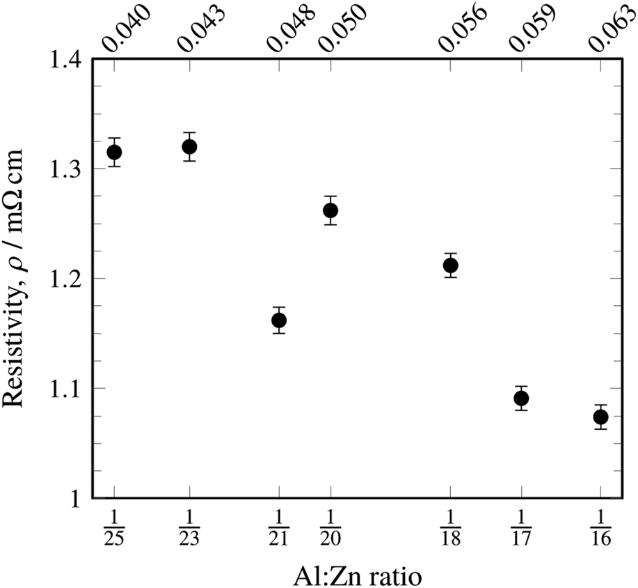
Figure 3: Resistivity of ALD-deposited AZO as a function of the Al:Zn atomic ratio as measured by EDX. Note that there was no significant difference in resistivity for the two recipes (see Fig. 2), and so, this chart includes data obtained from both recipes.
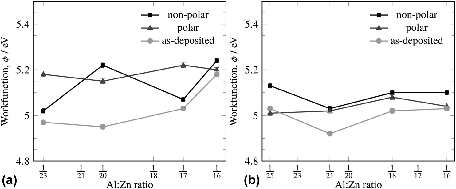
The work function of ZnO and AZO deposited by magnetron sputtering has previously been determined to be 4.71 eV and 4.62 eV, respectively [Reference Wei, Li, Deng and Deng20]. The work function of AZO deposited by magnetron sputtering was found to be 4.26 eV for UV-ozone treated AZO and 3.94 eV for acetone-treated AZO by ultraviolet photoelectron spectroscopy; the authors also reported that the work function was highly dependent on at.% content of Al and surface carbon content [Reference Wang, Feng, Jiang, Huang, Zhang, Song and Tan21]. These values are similar to the measured work functions we observed for ALD-deposited AZO. The work functions varied considerably depending on the surface treatment, which will be detailed in the following paragraphs. However, the average work functions for the surface recipe ranged between 5.06 and 5.21 eV, and for the ZnO-terminated recipe between 4.97 and 5.06 eV. Surface cleaning and immediate subsequent measurement of the surface were undertaken to assure a meaningful comparison between samples, but no distinct trend with respect to the measured dopant ratio was observed. Surface cleaning had a greater effect on the work function than the Al:Zn ratio of the film, and so, it is difficult to ascribe meaning to the minimum at the 1:21 doping level. This is not entirely surprising as Kelvin probe work function measurements are known to be very sensitive to surface treatment and relative humidity [Reference Özkanat, Salgin, Rohwerder, Mol, de Wit and Terryn22].
The measured work function was significantly affected by the terminal condition of the surface. When deposited with the Al-terminated recipe (i.e., a TMA pulse was the terminal pulse in the deposition), the as-deposited work function showed a range of 4.97 eV–5.18 eV, whereas the range of the as-deposited film using the ZnO-terminated recipe was 4.92–5.03 eV (Fig. 4). Different surface treatments (to clean the surface before measurement) also showed these trends. With an Al-terminated recipe, the polar treatment (terminating in water) gave a uniformly higher work function across all Al:Zn ratios, whereas the nonpolar treatment (toluene) gave more widely scattered work functions (Fig. 4). Because the Al-terminated recipe produces a surface with a high abundance of aluminum centers, aluminum oxide, aluminum hydroxide, zinc oxide, and zinc hydroxide moieties will all be present. It is likely that the distribution of polarities of the groups present at the surface alters the work function measurement significantly. When the ZnO-terminated recipe was used, the range of work functions dropped to 4.92–5.13 eV, regardless of the surface treatment used, and the polar rinse gave a uniform work function of 5.04 eV across all Al:Zn ratios within error.

Figure 4: The work functions of different Al:Zn atomic ratios with varying surface treatments for the Al-terminated (a) and ZnO-terminated (b) recipes (see Fig. 2). The light grey line (●) represents the as-deposited film, the black line (■) represents a nonpolar surface treatment, and the dark grey line (▲) represents the polar surface treatment.
Conclusions
Scanning Kelvin probe and four-point probe measurements revealed small but significant changes in the work functions and resistivities of doped zinc oxide films deposited by ALD. These changes were observed to result from two very different types of surface modification: The formulation of the ALD recipe used to generate the film and the solvents used to wash the film immediately before KP measurements. Two ALD pulse program recipes were used to establish the role that the TMA pulse placement plays in the films’ ultimate properties: One recipe terminated each DEZ/H2O subcycle with a TMA pulse and the other recipe buried the TMA pulse half-way into each DEZ/H2O subcycle. The TMA-terminated recipe generated films with, on average, higher work functions at Al:Zn ratios higher than 1:21, and lower resistivities at ratios above 1:19. The lowest resistivities observed were 1.05 mΩ cm for TMA-terminated films and 1.095 mΩ cm for the ZnO-terminated recipe, each with a 1:16 Al:Zn atomic ratio. The role of surface washing before work function measurement was elusive, and no clear trend could be established. The most significant difference observed was between washed and unwashed samples, regardless of the solvent used. Careful and detailed characterization of dopants and defects that contribute to electrical properties including the work function must be obtained if aluminum-doped zinc oxide is to fulfill its potential as a straightforward, earth-abundant, and environmentally friendly alternative to existing transparent conducting oxides.
Methods
ALD depositions were performed using a Picosun R200 Advanced deposition tool (Picosun OyMasalantie 365FI-02430 Masala, Finland). Trimethylaluminum (>98%) and diethylzinc (>95%) were purchased from Strem Chemicals, Inc., Newburyport, Massachusetts and used as received. These precursors and distilled water were held at 18 °C in stainless steel bubblers for all depositions. Purge and line flows used 99.998% N2 (150 sccm for TMA and DEZ, 200 sccm for water). The pulse and purge times for TMA, DEZ, and water were all 0.1 s and 6.0 s, respectively, for all depositions. In all depositions, the TMA pulse was introduced after a DEZ pulse/purge cycle, following the careful work reported by Na et al., who reported that this minimizes the impact of the TMA pulse on the growth rate [Reference Na, Peng, Scarel and Parsons15]. All depositions were performed with the chamber temperature set to 220 °C, with a measured temperature of 200 °C. This temperature was chosen as the minimum values for (undoped) ZnO film resistivity (10−3 Ω cm) are typically achieved in the range of 200–220 °C [Reference Tynell and Karppinen11]. To ascertain the impact on work function measurements, two pulse program recipes were used to generate the same dopant levels; in the first, the TMA pulse was introduced at the end of each DEZ/H2O subcycle. In the second recipe, the TMA pulse was introduced half-way through a DEZ/H2O subcycle. All substrates were 50 mm Si(100) wafers with a 1000 Å coating of thermally grown silica; this silica coating was essential for proper evaluation of the electrical properties of the deposited films as it provides a thick, robust, electrically insulating layer (Table II).
TABLE II: Pulse programs used for depositions. Each precursor identifier indicates a pulse/N2-purge pair. For example, the AZO (1:17) film used 76 supercycles, each consisting of 17 cycles of DEZ and water and one cycle of DEZ and TMA. Cycle values were chosen to deposit a film thickness of approximately 200 nm.

Ellipsometry was performed using a Plasmos SD2000 with a HeNe laser at λ = 632 nm. The refractive indices were set as follows: n Si = 3.882, (Palik, 1985)  ${n_{{\rm{Si}}{{\rm{o}}_{\rm{2}}}}}$ = 1.457, (Malitson, 1965), and n ZnO = 2.00.[Reference Madelung, Rössler and Schulz23] A refractive index of 2.00 was used for all ZnO and AZO films. The growth rates obtained from these measurements are in reasonable agreement with similar ALD processes in the literature [Reference Tynell and Karppinen11].
Elemental composition was determined using an Oxford Instruments/INCA energy dispersive spectroscopy system, installed on a Tescan Vega-II XMU Scanning Electron Microscope. All spectra were acquired using a beam acceleration of 20 kV, calibrated to a copper standard.
Sheet resistance was evaluated using a home-built four-point probe (4 PP), and resistivity values were determined from measurements of V, by Eq. (1) [Reference Smits24]
 $$\rho = {\pi / {{\rm{ln}}\left( 2 \right)\;{V / {I\;t}}}}\quad ,$$
where I was supplied by a constant current source set to 10 mA.
Work functions were measured with a KP Technology SKP5050 scanning Kelvin probe (sKP). The Au probe tip was set to vibrate at 75 Hz. The work function was measured as the sample was scanned over a 10 × 10 grid, taking points every 475 µm. The work function difference measured by the sKP was converted to an absolute sample work function by assuming a tip work function of 5.1 eV.
To ascertain the role of surface species remaining after cleaning, three independent sKP measurements were acquired after three separate surface treatments: (i) as deposited; (ii) a 5 s wash with toluene, hereafter referred to as the “nonpolar rinse”; and (iii) a series of 5 s washes of 2-propanol, ethanol, acetone, and water (the “polar rinse”). Each sample was thoroughly dried with flowing N2 at room temperature before measurement.


