Hostname: page-component-76fb5796d-5g6vh Total loading time: 0 Render date: 2024-04-26T08:51:16.664Z Has data issue: false hasContentIssue false

Selective diffusion of gold nanodots on nanopatterned substrates realized by self-assembly of diblock copolymers

Published online by Cambridge University Press:  20 January 2011

C. Garozzo
Affiliation:
Consiglio Nazionale delle Ricerche, Istituto per la Microelettronica e Microsistemi, Zona Industriale, 95121 Catania, Italy
R.A. Puglisi*
Affiliation:
Consiglio Nazionale delle Ricerche, Istituto per la Microelettronica e Microsistemi, Zona Industriale, 95121 Catania, Italy
C. Bongiorno
Affiliation:
Consiglio Nazionale delle Ricerche, Istituto per la Microelettronica e Microsistemi, Zona Industriale, 95121 Catania, Italy
S. Scalese
Affiliation:
Consiglio Nazionale delle Ricerche, Istituto per la Microelettronica e Microsistemi, Zona Industriale, 95121 Catania, Italy
E. Rimini
Affiliation:
Università di Catania, Dipartimento di Fisica, Catania, Italy
S. Lombardo
Affiliation:
Consiglio Nazionale delle Ricerche, Istituto per la Microelettronica e Microsistemi, Zona Industriale, 95121 Catania, Italy
*
a)Address all correspondence to this author. e-mail: rosaria.puglisi@imm.cnr.it
Get access

Abstract

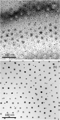
We investigated a simple and low-cost route for the formation of metallic nanodots on Si substrates ordered in size and position and laterally isolated by SiO2. The method was based on a two-step process: (i) the formation of a nanopattern of ordered cylindrical pores on oxidized Si substrates through self-assembly of diblock copolymers, and successive oxide dry etching down to the Si; (ii) the deposition of gold nanodots and thermal diffusion over the nanopatterned oxide substrates. After diffusion, the nanodot density outside the nanopores was found to decrease, and most of the nanodots were found to saturate the nanopores. The process was followed in situ by transmission electron microscopy (TEM) and ex situ by scanning electron microscopy (SEM) analysis for different thermal budgets. This patterned substrate can be used for catalyst mediated growth, for example, through vapor-liquid-solid (VLS), of nanowires for the formation of absorber materials in novel photovoltaic architectures.

Type
Reviews
Copyright
Copyright © Materials Research Society 2011

Access options

Get access to the full version of this content by using one of the access options below. (Log in options will check for institutional or personal access. Content may require purchase if you do not have access.)

References

REFERENCES

1.Kelzenberg, M.D., Boettcher, S.W., Petykiewicz, J.A., Turner-Evans, D.B., Putnam, M.C., Warren, E.L., Spurgeon, J.M., Briggs, R.M., Lewis, N.S., and Atwater, H.A.: Enhanced absorption and carrier collection in Si wire arrays for photovoltaic applications. Nat. Mater. 9, 239 (2010).CrossRefGoogle Scholar
2.Catchpole, K.R. and Polman, A.: Design principles for particle plasmon enhanced solar cells. Appl. Phys. Lett. 93, 191113 (2008).CrossRefGoogle Scholar
3.Maier, S.A.: Plasmonics—Fundamentals and Applications. (Springer, Berlin, 2007).CrossRefGoogle Scholar
4.Wagner, R.S. and Ellis, W.C.: Vapor-liquid-solid mechanism of single crystal growth. Appl. Phys. Lett. 4, 89 (1964).CrossRefGoogle Scholar
5.Givargizov, E.I.: Fundamental aspects of VLS growth. J. Cryst. Growth 31, 20 (1975).CrossRefGoogle Scholar
6.Kolasinski, K.W.: Catalytic growth of nanowires: Vapor–liquid–solid, vapor–solid–solid, solution–liquid–solid and solid–liquid–solid growth. Curr. Opin. Solid State Mater. Sci. 10, 182 (2006).CrossRefGoogle Scholar
7.Putnam, M.C., Filler, M.A., Kayes, B.M., Kelzenberg, M.D., Guan, Y., Lewis, N.S., Eiler, J.M., and Atwater, H.A.: Secondary ion mass spectrometry of vapor-liquid-solid grown, Au-catalyzed, Si wires. Nano Lett. 8, 3109 (2008).CrossRefGoogle ScholarPubMed
8.Perraud, S., Poncet, S., Noël, S., Levis, M., Faucherand, P., Rouvière, E., Thony, P., Jaussaud, C., and Delsol, R.: Full process for integrating silicon nanowire arrays into solar cells. Sol. Energy Mater. Sol. Cells 93, 1568 (2009).CrossRefGoogle Scholar
9.Latu-Romain, L., Mouchet, C., Cayron, C., Rouvière, E., and Simonato, J.P.: Growth parameters and shape specific synthesis of silicon nanowires by the VLS method. J. Nanopart. Res. 10, 1287 (2008).CrossRefGoogle Scholar
10.Irrera, A., Pecora, E.F., and Priolo, F.: Control of growth mechanisms and orientation in epitaxial Si nanowires grown by electron beam evaporation. Nanotechnology 20, 135601 (2009).CrossRefGoogle ScholarPubMed
11.Fan, H.J., Werner, P., and Zacharias, M.: Semiconductor nanowires: From self-organization to patterned growth. Small 2, 700 (2006).CrossRefGoogle ScholarPubMed
12.Yan, H.F., Xing, Y.J., Hang, Q.L., Yu, D.P., Wang, Y.P., Xu, J., Xi, Z.H., and Feng, S.Q.: Growth of amorphous silicon nanowires via a solid–liquid–solid mechanism. Chem. Phys. Lett. 323, 224 (2000).CrossRefGoogle Scholar
13.Yu, D.P., Xing, Y.J., Hang, Q.L., Yan, H.F., Xu, J., Xi, Z.H., and Feng, S.Q.: Controlled growth of oriented amorphous silicon nanowires via a solid–liquid–solid (SLS) mechanism. Physica E 9, 305 (2001).CrossRefGoogle Scholar
14.Guarini, K.W., Black, C.T., and Yeung, S.H.I.: Optimization of diblock copolymer thin film self assembly. Adv. Mater. 14(18), 1290 (2002).3.0.CO;2-N>CrossRefGoogle Scholar
15.Thurn-Albrecht, T., Schotter, J., Kastle, G.A., Emley, N., Shibauchi, T., Krusin-Elbaum, L., Guarini, K., Black, C.T., Tuominen, M.T., and Russell, T.P.: Ultrahigh-density nanowire arrays grown in self-assembled diblock copolymer templates. Science 290, 2126 (2000).CrossRefGoogle ScholarPubMed
16.Kim, S.J., Maeng, W.J., Lee, S.K., Park, D.H., Bang, S.H., Kima, H., and Sohn, B.H.: Hybrid nanofabrication processes utilizing diblock copolymer nanotemplate prepared by self-assembled monolayer based surface neutralization. J. Vac. Sci. Technol., B 26(1), 189 (2008).CrossRefGoogle Scholar
17.Guarini, K.W., Black, C.T., Zhang, Y., Kim, H., Sikorski, E.M., and Babich, I.V.: Process integration of self-assembled polymer templates into silicon nanofabrication. J. Vac. Sci. Technol., B 20(6), 2788 (2002).CrossRefGoogle Scholar
18.Guarini, K.W., Black, C.T., Milkove, K.R., and Sandstrom, R.L.: Nanoscale patterning using self-assembled polymers for semiconductor applications. J. Vac. Sci. Technol., B 19(6), 2784 (2001).CrossRefGoogle Scholar
19.La Fata, P., Puglisi, R., Lombardo, S., and Bongiorno, C.: Nano-patterning with block copolymers. Superlattices Microstruct. 44, 693 (2008).CrossRefGoogle Scholar
20.Puglisi, R.A., Scandurra, A., Bongiorno, C., La Fata, P., and Lombardo, S.: Pattern transfer of nanomasks based on diblock copolymers through reactive ion etching (to be submitted).Google Scholar
21.Mansky, P., Liu, Y., Huang, E., Russell, T.P., and Hawker, C.: Controlling polymer-surface interactions with random copolymer brushes. Science 275, 1458 (1997).CrossRefGoogle Scholar
22.Puglisi, R.A., La Fata, P., and Lombardo, S.: Tailoring the long-range order of block copolymer based nanomasks on flat substrates. Appl. Phys. Lett. 91, 053104 (2007).CrossRefGoogle Scholar
23.Ruffell, S., Venkatachalam, D.K., Shalav, A., and Elliman, R.G.: Formation of ordered arrays of gold particles on silicon and silicon-dioxide by nanoindentation patterning, in Nanoscale Pattern Formation, edited by Chason, E., Cuerno, R., Gray, J., and Heinig, K.-H. (Mater. Res. Soc. Symp. Proc. 1228E, Warrendale, PA, 2010), 1228-KK13-05.Google Scholar
24.Venables, J.A.: Atomic processes in crystal growth. Surf. Sci. 299/300, 798 (1994).CrossRefGoogle Scholar
25.Ruffino, F., Grimaldi, M.G., Bongiorno, C., Giannazzo, F., Roccaforte, F., and Raineri, V.: Microstructure of Au nanoclusters formed in and on SiO2. Superlattices Microstruct. 44, 588 (2008).CrossRefGoogle Scholar
26.Allen, J.E., Hemesath, E.R., Perea, D.E., Lensch-Falk, J.L., Li, Z.Y., Yin, F., Gass, M.H., Wang, P., Bleloch, A.L., Palmer, R.E., and Lauhon, L.J.: High-resolution detection of Au catalyst atoms in Si nanowires. J. Nat. Nanotechol. 3, 168 (2008).CrossRefGoogle ScholarPubMed
27.Bullis, W.M.: Properties of gold in silicon. Solid-State Electron. 9(2), 143 (1966).CrossRefGoogle Scholar