


I. INTRODUCTION
A well-known revolutionary 2-dimensional (2D) material graphene has been widely explored since its discovery to investigate its fundamental physics to find its applicability in practical applications. Among many remarkable properties, graphene’s good transport properties, and high thermo-mechanical properties have proven its strong suitability in nanoelectronics and photonics. However, symmetrical electrical band structure of semi-metallic graphene at Dirac point, i.e., zero band gap energy limits its use for many optoelectronic applications. Therefore, many remarkable efforts have been done to increase its band gap (E g). Reference Lee, Duong, Vu, Jin, Kim and Lee1–Reference Han, Ozyilmaz, Zhang and Kim6 To address these issues, simultaneously, a lot of research has been made toward semiconducting materials such as transition metal dichalcogenides (TMDs) and insulating materials such as hexagonal boron nitride (h-BN), silicene, and phosphorene, at quite a rapid pace. Among 2D family of materials, phosphorene, a single atomic layer of black phosphorus (BP), has recently attracted significant attention due to its interesting strong angle dependent opto-electronic properties and anisotropic characteristics. In particular, by filling the large gap of unresolved properties such as energy gap, Reference Dvorak, Oswald and Wu4,Reference Han, Ozyilmaz, Zhang and Kim6–Reference Kim, Baik, Ryu, Sohn, Park, Park, Denlinger, Yi, Choi and Kim11 charge carrier mobility, Reference Bolotin, Sikes, Jiang, Klima, Fudenberg, Hone, Kim and Stormer12–Reference Wu, De, Chang, Wang, Peng, Bao and Pei16 current on/off ratio Reference Wu, De, Chang, Wang, Peng, Bao and Pei16–Reference Liu, Neal, Zhu, Luo, Xu, Tománek and Ye18 and response time Reference Urich, Unterrainer and Mueller19,Reference Buscema, Groenendijk, Blanter, Steele, van der Zant and Castellanos-Gomez20 between graphene and TMDs, this unique feature is coming to the forefront of next generation nano-sized electronic devices.
Above all, a widely tunable band gap (E g) of phosphorene is one of the great advantages in 2D regimes, and this interesting electronic structure induces light-matter optical interaction with very broad spectral range from the visible to infrared region. Theoretical calculations Reference Tran, Soklaski, Liang and Yang21 and experimental data Reference Li, Kim, Jin, Ye, Qiu, da Jornada, Shi, Chen, Zhang and Yang22–Reference Das, Zhang, Demarteau, Hoffmann, Dubey and Roelofs24 show that the layer-dependent direct E g of black phosphorus (a few layer of phosphorene) compared to graphene and TMD semiconductors ranges broadly from 0.3 to 2.05 eV. In this sizable value, it can be further controlled using various methods, for instance, mechanical stress, Reference Peng, Wei and Copple25,Reference Sa, Li, Qi, Ahuja and Sun26 electrical field, Reference Das, Zhang, Demarteau, Hoffmann, Dubey and Roelofs24 dimensional size control, Reference Woomer, Farnsworth, Hu, Wells, Donley and Warren27 edge oxidation, Reference Ziletti, Carvalho, Trevisanutto, Campbell, Coker and Neto28,Reference Lu, Wu, Carvalho, Ziletti, Liu, Tan, Chen, Castro Neto, Özyilmaz and Sow29 different stacking orders, Reference Dai and Zeng30 hetero structure with other 2D materials, Reference Padilha, Fazzio and da Silva31,Reference Hu and Hong32 and substitutional doping. Reference Koenig, Doganov, Seixas, Carvalho, Tan, Watanabe, Taniguchi, Yakovlev, Castro Neto and Özyilmaz33,Reference Kulish, Malyi, Persson and Wu34 For layer dependency, the single layer has a noticeable E g ∼2.0 eV, but it gradually decreases to 0.3 eV as increasing film thickness to bulk size which is explained by the harmonized effect of interlayer coupling and quantum confinement effect. Reference Takagahara and Takeda35 In addition, unlike the indirect to direct band gap transition in TMDs, the band structure of phosphorene remains direct at the Γ point of Brillouin zone as increasing thickness up to few-layer. Only in bulk BP, conduction band minimum and valence band maximum are detected at the Z point. This stable and thickness independent band topology is very beneficial for its potential photonics and optoelectronics in nano scale 2D regime.
The puckered lattice structure of phosphorene as shown in Figs. 1(a) and 1(b) leads to in-plane anisotropic physical properties including thermal conductivity, Reference Qin, Yan, Qin, Yue, Hu and Su36 Young’s modulus Reference Liu, Neal, Zhu, Luo, Xu, Tománek and Ye18,Reference Peng, Wei and Copple25,Reference Wei and Peng37,Reference Wang, Kutana, Zou and Yakobson38 carrier mobility and effective masses, Reference Wang, Kutana, Zou and Yakobson38,Reference Qiao, Kong, Hu, Yang and Ji39 and exciton dynamics, Reference Zhang, Yang, Xu, Wang, Li, Ghufran, Zhang, Yu, Zhang and Qin40–Reference Tran, Soklaski, Liang and Yang43 which are in marked contrast to those of graphene and TMDs. Highly anisotropic natures extended the prospect of phosphorene for a broad range of optical applications with a precedently unrevealed sizable band gap. Consequently, to optimize the designed phosphorene optical sensors with high-efficiency, it becomes critical to determine the right orientation on the substrates as well as to select the interlayer stacking orders. Notwithstanding the promising candidates of post graphene 2D materials as introduced, phosphorene is unstable and prone to oxidation promptly in ambient conditions in contrast to graphene, Reference Ziletti, Carvalho, Campbell, Coker and Neto44 which degrades a lifecycle in most of electrical devices. Thus, new passivation methods were announced using Al2O3, Reference Luo, Rahbarihagh, Hwang, Liu, Du and Peide45–Reference Pei, Gai, Yang, Wang, Yu, Choi, Luther-Davies and Lu47 graphene, Reference Avsar, Vera-Marun, Tan, Watanabe, Taniguchi, Castro Neto and Ozyilmaz48 h-BN, Reference Hu and Hong32 or hydrophobic polymer Reference Bao, Cai, Kim, Sridhara and Fuhrer49–Reference Zhu, Yogeesh, Yang, Aldave, Kim, Sonde, Tao, Lu and Akinwande51 as a passivation layer, and more aggressively phosphorus oxide (P x O y ) layers similar to SiO2 on Si substrate could be used as a functional material in single- or few-layer at the pristine BP surface. Reference Pei, Gai, Yang, Wang, Yu, Choi, Luther-Davies and Lu47

FIG. 1. Atomic structure and layer dependent characteristics of black phosphorus. (a) Schematic diagram of black phosphorus layer structure. (b) Microscope image of 1L phosphorene. (c) Calculated band structure by DFT (dashed lines) and GW-BSE (solid lines) for monolayer phosphorene. (d) OPL values from simulation (black dots) and experimental PSI measurements (red dots) for black phosphorus layers from 1L to 6L. (e) PL spectra of the 1L–5L phosphorene flakes. PL intensities are normalized, and the emission peak of the PL spectrum for monolayer is at 711 nm, corresponding to peak energy of 1.75 eV. (f) Evolution of PL peak energy with layer number of phosphorene. The PL for the monolayer was measured at −10 °C, while others were measured at room temperature. Inset: schematic energy diagram showing the electronic band gap (E g), optical gap (E opt), and the exciton binding energy (E b). Parts (b), (d), (e), and (f) are adapted with permission Ref. Reference Yang, Xu, Pei, Myint, Wang, Wang, Zhang, Yu and Lu54. Parts (c) is adapted with permission from Ref. Reference Tran, Soklaski, Liang and Yang21.
In this perspective, we present the recent advances in the unique optical characteristics of phosphorene, such as anisotropic luminescence, light-matter interaction, tunable E g and exciton emissions, and also discuss challenges for its practical applications to current nano-technology. Finally, the state of the art of opto-electrical sensing devices based on BP is introduced.
II. ELECTRICAL STRUCTURE AND LAYER DEPENDENT OPTICAL PROPERTIES
Bulk black phosphorus (BP) consists of infinite number of phosphorene monolayers similar to graphene and other 2D materials, and the 2D flat layers are weakly coupled by the van der Waals force which allows to exfoliate BP into phosphorene nano-sheets. Reference Appalakondaiah, Vaitheeswaran, Lebegue, Christensen and Svane52 However, unlike in other 2D materials, phosphorene does not form entirely flat sheets like but it constructs a puckered surface structure due to the sp 3 hybridization. Based on pre-revealed 2D materials atomic crystalline structure, phosphorene’s ridged surface is normally defined as x axis—zigzag direction and y axis—armchair direction.
From the perspective of semiconducting applications, since the electronic band gap structure is a fundamental factor, it is theoretically calculated by using first-principles density functional theory (DFT) and GW-Bethe–Salpeter equation (BSE) [Fig. 1(c)] Reference Tran, Soklaski, Liang and Yang21 and also experimentally measured by using photoluminescence excitation spectroscopy ranging from 0.3 eV in bulk to ∼2.0 eV in monolayer. This sizable value is obviously thickness dependent, and induced exciton binding energy and optical absorption are also controllable with different thickness in contrast to other 2D layered materials.
Few-layer phosphorene has only several atoms in thickness, but the PL intensities from 2L to 5L layered phosphorene are all stronger than that from the thick Si substrate. This is because of the direct band gap structure in few-layer phosphorene and the indirect band gap in Si. As compared to the indirect band gap behaviors in TMDs, Reference Ramasubramaniam, Naveh and Towe8,Reference Wu, Qu and MacDonald53 this intrinsic direct band gap nature in few-layer phosphorene serves them great potential advantages for various optoelectronic applications.
Layer thickness of nano-sheets can be calculated using Kelvin probe force microscope (KPFM) but it has a risk to damage the delicate sample surfaces by the sharp scanning tip during the measurement. Recently, optical path length (OPL) of the light reflected from the 2D layer is introduced as a fast, non-invasive, and highly accurate technique to measure the thickness and the atomic layer number of BP.
Reference Yang, Xu, Pei, Myint, Wang, Wang, Zhang, Yu and Lu54
The OPL is calculated from the relation,
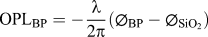 ${\rm{OP}}{{\rm{L}}_{{\rm{BP}}}} = - {\lambda \over {2\pi }}\left( {{\emptyset _{{\rm{BP}}}} - {\emptyset _{{\rm{Si}}{{\rm{O}}_2}}}} \right)$
, where λ is the wave length of the light source, and ∅BP and
${\rm{OP}}{{\rm{L}}_{{\rm{BP}}}} = - {\lambda \over {2\pi }}\left( {{\emptyset _{{\rm{BP}}}} - {\emptyset _{{\rm{Si}}{{\rm{O}}_2}}}} \right)$
, where λ is the wave length of the light source, and ∅BP and
 ${\emptyset _{{\rm{Si}}{{\rm{O}}_2}}}$
are the phase shift of the light reflected from the BP and SiO2/Si substrate, respectively. In experiment, phase-shifting interferometry (PSI) using very low-density light from a light-emitting diode (LED) is used to measure the OPL. OPL values obtained from simulations and experiments for BP from 1L to 6L are linearly fit well as shown in Fig. 1(d).
${\emptyset _{{\rm{Si}}{{\rm{O}}_2}}}$
are the phase shift of the light reflected from the BP and SiO2/Si substrate, respectively. In experiment, phase-shifting interferometry (PSI) using very low-density light from a light-emitting diode (LED) is used to measure the OPL. OPL values obtained from simulations and experiments for BP from 1L to 6L are linearly fit well as shown in Fig. 1(d).
With the evolution of the electronic band structure on low-dimensional materials, the induced exciton, a bound quasiparticle state between electron and hole through a Coulomb force, plays a key role to understand the relation between variant effects of the spacial dimension, shape, crystalline structure, and material composition on the nano-optoelectronic properties. Figure 1(e) shows the normalized PL spectra of the 1L–5L phosphorene flakes. The emission peak of the PL spectrum for monolayer phosphorene is at 711 nm, corresponding to the peak energy of 1.75 eV. The peak energy of PL emission, which is termed as optical gap (E opt), is the difference between the electronic band gap (E g) and the exciton binding energy (E b) [Fig. 1(f) inset]. Strong quantum confinement effect at free-standing monolayer phosphorene induces a large exciton binding energy of ∼0.8 eV, Reference Tran, Soklaski, Liang and Yang21,Reference Rodin, Carvalho and Neto55 whereas this value for monolayer phosphorene on a SiO2/Si substrate is measured to be only ∼0.3 eV on account of the increased screening effect from the substrate. Reference Rodin, Carvalho and Neto55 A high exciton binding energy stabilizes excitons and trions (charged excitons) against thermal fluctuations which conventionally degrade the transport efficiency in opto–electronic devices.
As depicted in Fig. 1(f), the optical gaps in phosphorene layers increase rapidly with decreasing layer number because of the strong quantum confinement effect and the van der Waals force between the phosphorene layers.
Reference Yang, Xu, Pei, Myint, Wang, Wang, Zhang, Yu and Lu54
A nonlinear curve by fitting the measured optical gaps is obtained as
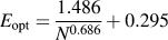 ${E_{{\rm{opt}}}} = {{1.486} \over {{N^{0.686}}}} + 0.295$
, where E
opt is the optical gap in unit of eV and N is the layer number, and this layer-dependent optical gap function agree well with the theoretical models.
Reference Tran, Soklaski, Liang and Yang21
For bulk phosphorene sample with infinite N value, its optical gap converges the limit value of ∼0.295 eV, which perfectly matches well with the measured energy gap (∼0.3 eV) of bulk phosphorus.
Reference Li, Yu, Ye, Ge, Ou, Wu, Feng, Chen and Zhang56,Reference Keyes57
${E_{{\rm{opt}}}} = {{1.486} \over {{N^{0.686}}}} + 0.295$
, where E
opt is the optical gap in unit of eV and N is the layer number, and this layer-dependent optical gap function agree well with the theoretical models.
Reference Tran, Soklaski, Liang and Yang21
For bulk phosphorene sample with infinite N value, its optical gap converges the limit value of ∼0.295 eV, which perfectly matches well with the measured energy gap (∼0.3 eV) of bulk phosphorus.
Reference Li, Yu, Ye, Ge, Ou, Wu, Feng, Chen and Zhang56,Reference Keyes57
III. ANISOTROPIC OPTICAL PROPERTIES
The atomic crystal structure of phosphorene possesses a puckered orthorhombic lattice with the D
2h group point symmetry.
Reference Li and Appelbaum58
The lattice parameters along the two perpendicular directions are respectively |a
1| = 4.37 Å, |a
2| = 3.31 Å.
Reference Li and Appelbaum58
Due to its notable nonplanar, ridged structural shape, phosphorene shows anisotropic natures of electronic, optoelectronic, phononic, and thermo-electronic properties. These properties are principally affected by the carrier mobility (µ), which is inversely proportional to the effective masses
 $\left( {{m^*}} \right)$
as
$\left( {{m^*}} \right)$
as
 ${\rm{ = }}q\tau /{m^*}$
, where τ is the scattering time and q is the charge. The anisotropic effective mass values of carriers along zigzag (x) and armchair (y) directions at phosphorene are calculated
Reference Qiao, Kong, Hu, Yang and Ji39
:
${\rm{ = }}q\tau /{m^*}$
, where τ is the scattering time and q is the charge. The anisotropic effective mass values of carriers along zigzag (x) and armchair (y) directions at phosphorene are calculated
Reference Qiao, Kong, Hu, Yang and Ji39
:
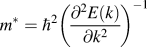 ${m^*} = {\hbar ^2}{\left( {{{{\partial ^2}E\left( k \right)} \over {\partial {k^2}}}} \right)^{ - 1}}$
, where k is the reciprocal lattice vector and E is the energy, and
${m^*} = {\hbar ^2}{\left( {{{{\partial ^2}E\left( k \right)} \over {\partial {k^2}}}} \right)^{ - 1}}$
, where k is the reciprocal lattice vector and E is the energy, and
 $m_{{\rm{c,}}\,{\rm{zig}}}^*$
is up to ∼10 times heavier than
$m_{{\rm{c,}}\,{\rm{zig}}}^*$
is up to ∼10 times heavier than
 $m_{{\rm{c,}}\,{\rm{arm}}}^*$
indicating that the armchair direction is much more efficient for carrier transport.
$m_{{\rm{c,}}\,{\rm{arm}}}^*$
indicating that the armchair direction is much more efficient for carrier transport.
The polarization angle dependency of phonon dynamics was simply measured using Raman spectroscopy. As shown in Fig. 2(a), Raman scattering intensities exhibit
 ${\rm{A}}_{\rm{g}}^{\rm{1}}$
,
${\rm{A}}_{\rm{g}}^{\rm{1}}$
,
 ${{\rm{B}}_{{\rm{2g}}}}$
, and
${{\rm{B}}_{{\rm{2g}}}}$
, and
 ${\rm{A}}_{\rm{g}}^{\rm{2}}$
phonon modes along the z, y, and x directions in phosphorene flakes respectively. Intensity of
${\rm{A}}_{\rm{g}}^{\rm{2}}$
phonon modes along the z, y, and x directions in phosphorene flakes respectively. Intensity of
 ${{\rm{B}}_{{\rm{2g}}}}$
(armchair) and
${{\rm{B}}_{{\rm{2g}}}}$
(armchair) and
 ${\rm{A}}_{\rm{g}}^{\rm{2}}$
(zigzag) modes are significantly dependent on the polarization angle by showing an angle period of 180° [Fig. 2(b)]. Each two modes generate maximum value when the laser polarization is parallel (0°) with its crystalline direction, while the intensity reaches minimum when it is crossing right angle (90°). However, since
${\rm{A}}_{\rm{g}}^{\rm{2}}$
(zigzag) modes are significantly dependent on the polarization angle by showing an angle period of 180° [Fig. 2(b)]. Each two modes generate maximum value when the laser polarization is parallel (0°) with its crystalline direction, while the intensity reaches minimum when it is crossing right angle (90°). However, since
 ${\rm{A}}_{\rm{g}}^{\rm{1}}$
mode oscillates along z-direction, it is not sensitive to the angle of laser polarization.
Reference Zhang, Yang, Xu, Wang, Li, Ghufran, Zhang, Yu, Zhang and Qin40
Furthermore, the lab-designed polarized optical microscope revealed optical anisotropy of few-layer BP in the visible regime.
Reference Mao, Tang, Xie, Wu, Han, Lin, Deng, Ji, Xu and Liu59
Optical contrast in the RGB channels of BP exhibits periodic variation with the rotation angles from 0 to 180° [Figs. 2(c) and 2(d)]. These simple and accurate methods are optimized to determine the atomic crystalline orientation of phosphorene layers, and it will touch up the nano-measurement technologies for other anisotropic 2D layered structures.
${\rm{A}}_{\rm{g}}^{\rm{1}}$
mode oscillates along z-direction, it is not sensitive to the angle of laser polarization.
Reference Zhang, Yang, Xu, Wang, Li, Ghufran, Zhang, Yu, Zhang and Qin40
Furthermore, the lab-designed polarized optical microscope revealed optical anisotropy of few-layer BP in the visible regime.
Reference Mao, Tang, Xie, Wu, Han, Lin, Deng, Ji, Xu and Liu59
Optical contrast in the RGB channels of BP exhibits periodic variation with the rotation angles from 0 to 180° [Figs. 2(c) and 2(d)]. These simple and accurate methods are optimized to determine the atomic crystalline orientation of phosphorene layers, and it will touch up the nano-measurement technologies for other anisotropic 2D layered structures.

FIG. 2. Anisotropic optical properties of black phosphorus. (a) Raman spectrum of 2L phosphorene. Inset: the vibration directions of
 ${\rm{A}}_{\rm{g}}^{\rm{1}}$
,
${\rm{A}}_{\rm{g}}^{\rm{1}}$
,
 ${{\rm{B}}_{{\rm{2g}}}}$
, and
${{\rm{B}}_{{\rm{2g}}}}$
, and
 ${\rm{A}}_{\rm{g}}^{\rm{2}}$
Raman modes. (b) Polarization dependence of
${\rm{A}}_{\rm{g}}^{\rm{2}}$
Raman modes. (b) Polarization dependence of
 ${\rm{A}}_{\rm{g}}^{\rm{1}}$
,
${\rm{A}}_{\rm{g}}^{\rm{1}}$
,
 ${{\rm{B}}_{{\rm{2g}}}}$
, and
${{\rm{B}}_{{\rm{2g}}}}$
, and
 ${\rm{A}}_{\rm{g}}^{\rm{2}}$
modes in a 15L phosphorene and silicon substrate. The intensities of
${\rm{A}}_{\rm{g}}^{\rm{2}}$
modes in a 15L phosphorene and silicon substrate. The intensities of
 ${{\rm{B}}_{{\rm{2g}}}}$
and
${{\rm{B}}_{{\rm{2g}}}}$
and
 ${\rm{A}}_{\rm{g}}^{\rm{2}}$
modes both show the apparent angle dependent curves. (c) Optical images of a thick black phosphorus sample shows a color change as a function of rotation angle, and (d) RGB optical intensities of the reflected light in the region marked with red square in (c) exhibit sinusoidal behaviors. (e) Top view of the square of the electron wavefunction of the bright ground-state exciton in monolayer phosphorene. Since the carriers are more mobile along the x direction with low effective mass and the Coulomb interaction is isotropic, the exciton is anisotropic forming striped patterns. (f) The measured PL quenching factor from the 2L phosphorene. The red line is the fitted sinusoidal function of emission polarization angle. (g) Photoluminescence peak intensity as a function of polarization detection angle for excitation laser polarized along x (gray), 45° (magenta) and y (blue) directions. Parts (a) and (b) are adapted with permission Ref. Reference Zhang, Yang, Xu, Wang, Li, Ghufran, Zhang, Yu, Zhang and Qin40. Parts (c) and (d) are adapted with permission Ref. Reference Mao, Tang, Xie, Wu, Han, Lin, Deng, Ji, Xu and Liu59. Parts (e) and (g) are adapted with permission Ref. Reference Wang, Jones, Seyler, Tran, Jia, Zhao, Wang, Yang, Xu and Xia41. Part (f) is adapted with permission with Ref. Reference Xu, Yang, Zhu, Yan, Pei, Myint, Zhang and Lu23.
${\rm{A}}_{\rm{g}}^{\rm{2}}$
modes both show the apparent angle dependent curves. (c) Optical images of a thick black phosphorus sample shows a color change as a function of rotation angle, and (d) RGB optical intensities of the reflected light in the region marked with red square in (c) exhibit sinusoidal behaviors. (e) Top view of the square of the electron wavefunction of the bright ground-state exciton in monolayer phosphorene. Since the carriers are more mobile along the x direction with low effective mass and the Coulomb interaction is isotropic, the exciton is anisotropic forming striped patterns. (f) The measured PL quenching factor from the 2L phosphorene. The red line is the fitted sinusoidal function of emission polarization angle. (g) Photoluminescence peak intensity as a function of polarization detection angle for excitation laser polarized along x (gray), 45° (magenta) and y (blue) directions. Parts (a) and (b) are adapted with permission Ref. Reference Zhang, Yang, Xu, Wang, Li, Ghufran, Zhang, Yu, Zhang and Qin40. Parts (c) and (d) are adapted with permission Ref. Reference Mao, Tang, Xie, Wu, Han, Lin, Deng, Ji, Xu and Liu59. Parts (e) and (g) are adapted with permission Ref. Reference Wang, Jones, Seyler, Tran, Jia, Zhao, Wang, Yang, Xu and Xia41. Part (f) is adapted with permission with Ref. Reference Xu, Yang, Zhu, Yan, Pei, Myint, Zhang and Lu23.
In particular, excitons in phosphorene are predicted to be confined in a quasi-one-dimensional (1D) space due to its anisotropic nature, in contrast to other 2D materials such as graphene and TMDs, so it provides an ideal platform for investigating remarkable exciton dynamics in a reduced regime. Especially, excitons at phosphorene are characterized that their spatial distribution of wave functions is anisotropic by intensely extending along the armchair direction.
Reference Wang, Jones, Seyler, Tran, Jia, Zhao, Wang, Yang, Xu and Xia41
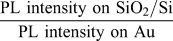
Figure 2(e) displays the simulated wave function of the bright ground-state exciton. This result is associated with the consequence of the directional mass dependence, and the isotropic Coulomb interaction binds the carriers most strongly in the zigzag direction. Experimentally, the excitons are measured by capturing the linearly polarized excitons using angle-resolved PL spectroscopy. For example, charge transfer dynamics has been determined in a phosphorene-gold hybrid system where the bilayered phosphorene flake is transferred on a gold pad, which is patterned on SiO2/Si substrate.
Reference Xu, Yang, Zhu, Yan, Pei, Myint, Zhang and Lu23
The maximum PL intensities at 945 nm from phosphorene on Au and SiO2/Si substrate show a big different value and large in-plane anisotropy along the emission polarization angle. A quenching factor defined by
 ${{{\rm{PL\ intensity\ on\ Si}}{{\rm{O}}_2}/{\rm{Si}}} \over {{\rm{PL\ intensity\ on\ Au}}}}$
is used to describe the exciton dynamics, and the plotted data presents a well fitted curve by a sinusoidal function with a period of ∼180° as shown in Fig. 2(f). Simultaneously, anisotropic nature of trions have also been observed with an extraordinarily large binding energy of ∼162 meV
Reference Xu, Zhang, Wang, Yang, Wang, Pei, Myint, Xing, Yu and Fu42
which is approximately 1 order of magnitude higher than those in 2D TMDs.
Reference Zhang, Yang, Xu, Wang, Li, Ghufran, Zhang, Yu, Zhang and Qin40,Reference Li, Yu, Ye, Ge, Ou, Wu, Feng, Chen and Zhang56
Furthermore, this intriguing PL observations are consistent in monolayer phosphorene,
Reference Wang, Jones, Seyler, Tran, Jia, Zhao, Wang, Yang, Xu and Xia41
in which the PL intensity along the y direction is steadily less than 3% of that along the x direction [Fig. 2(g)] regardless of the excitation laser polarization.
${{{\rm{PL\ intensity\ on\ Si}}{{\rm{O}}_2}/{\rm{Si}}} \over {{\rm{PL\ intensity\ on\ Au}}}}$
is used to describe the exciton dynamics, and the plotted data presents a well fitted curve by a sinusoidal function with a period of ∼180° as shown in Fig. 2(f). Simultaneously, anisotropic nature of trions have also been observed with an extraordinarily large binding energy of ∼162 meV
Reference Xu, Zhang, Wang, Yang, Wang, Pei, Myint, Xing, Yu and Fu42
which is approximately 1 order of magnitude higher than those in 2D TMDs.
Reference Zhang, Yang, Xu, Wang, Li, Ghufran, Zhang, Yu, Zhang and Qin40,Reference Li, Yu, Ye, Ge, Ou, Wu, Feng, Chen and Zhang56
Furthermore, this intriguing PL observations are consistent in monolayer phosphorene,
Reference Wang, Jones, Seyler, Tran, Jia, Zhao, Wang, Yang, Xu and Xia41
in which the PL intensity along the y direction is steadily less than 3% of that along the x direction [Fig. 2(g)] regardless of the excitation laser polarization.
Basically these anisotropic properties are originated from the unique atomic structure of phosphorene. Additionally, apart from those distinct electro-optical properties, phosphorene also exhibits strong directional dependent physical properties in thermal conductivity and mechanical strain behaviors. By understanding the anisotropic nature of this emerging material, we can discover more interesting physical phenomena in 2D layered heterostructure and its potential applications.
IV. HIGH-PERFORMANCE PHOTO DETECTORS BASED ON BLACK PHOSPHOROUS
Intensive research efforts on the BP have led to high-performance photo sensing devices. As described on this Review, black phosphorus (BP) can satisfy both criterions on the electric- and optical-requirements as a next generation material with far-reaching potentials. Basically, photodetection ability relies on the transformation of absorbed photons into an electrical signal. Highly advanced photodetector based on FET using few-layered BP (Fig. 3(a)) presents a remarkably fast time response Reference Buscema, Groenendijk, Blanter, Steele, van der Zant and Castellanos-Gomez20 : rise (τrise) and fall (τfall) time to be 1 ms and 4 ms, respectively as shown in Fig. 3(c). According to the wide range of the tunable band gap on BP, photodetector operates across the visible and up to the near-infrared (NIR) regions (940 nm) [Fig. 3(b)]. However, as summarized in Table I, TMDs and semiconducting layered materials exhibit relatively slow photoresponse because of the large band gap; they are limited near the visible range of the spectrum.

FIG. 3. Black phosphorus (BP) based photo-detecting sensors. (a) Configuration of the fast photoresponse sensing device based on BP-FET. (b) Measured photocurrent responses from the BP-FET for different wavelengths (λ) 640, 808, and 940 nm. Peak value decreases with increasing wave length, and (c) photocurrent intensity in one period of light excitation [λ = 640 nm, incident power (P d) = 6.49 µW] exhibits very fast rise and fall response time (1 ms and 4 ms). (d) BP based photodetector with high responsivity (R) and (e) its 3D topography. (f and g) Responsivity of the detector at different incident laser power. The wave length of the laser is 633 and 900 nm in part (f) and (g), respectively. A high photoresponsivity R = 6.7 × 10⁵ A/W for 633 nm, and 7.0 × 10⁶ A/W for 900 nm both at 20 K condition. Parts (a), (b), and (c) are adapted with permission Ref. Reference Buscema, Groenendijk, Blanter, Steele, van der Zant and Castellanos-Gomez20. Parts (d), (e), (f), and (g) are adapted with permission Ref. Reference Huang, Wang, Chen, Ma, Li, Han and Wu60.
TABLE I. Comparison of figures-of-merit for photodetectors based on 2D materials. Adapted from Ref. Reference Buscema, Groenendijk, Blanter, Steele, van der Zant and Castellanos-Gomez20 with permission.

Recently, BP photodetector based on backgate FET high photoresponsivity
Reference Huang, Wang, Chen, Ma, Li, Han and Wu60
in a broad range from visible (400 nm) to NIR (900 nm) has been introduced as shown in Figs. 3(d) and 3(e). They drastically increased the level of photoresponsivity to be 7 × 10⁶ A/W at 20 K and 4.3 × 10⁶ A/W at 300 K for the 100 nm channel length in a broadband spectrum [Figs. 3(f) and 3(g)]. This device shows also high response time (rise) with τrise = 5 ms. A simplified relationship of responsivity against channel length agrees well with the experimental measurement, since the photoresponsivity (R) can be expressed as
 $R \propto {{{\tau _{{\rm{lifetime}}}}} \over {{\tau _{{\rm{transit}}}}}}$
, where τlifetime is the lifetime of the photo-induced carrier, τtransit is the carrier transfer time. Here, the transient time is provided by
$R \propto {{{\tau _{{\rm{lifetime}}}}} \over {{\tau _{{\rm{transit}}}}}}$
, where τlifetime is the lifetime of the photo-induced carrier, τtransit is the carrier transfer time. Here, the transient time is provided by
 ${\tau _{{\rm{transit}}}} = {{{L^2}} \over {\mu {V_{{\rm{ds}}}}}}$
, where L is the channel length, µ is the carrier mobility, and V
ds is the drain-source voltage.
${\tau _{{\rm{transit}}}} = {{{L^2}} \over {\mu {V_{{\rm{ds}}}}}}$
, where L is the channel length, µ is the carrier mobility, and V
ds is the drain-source voltage.
V. CHALLENGES AND FUTURE RESEARCH DIRECTIONS
Despite of the fact that phosphorene can be a new material in the ‘post-graphene age’ it is relatively vulnerable against environmental attack due to its tendency to oxidize in ambient conditions. Reference Ziletti, Carvalho, Campbell, Coker and Neto44,Reference Wood, Wells, Jariwala, Chen, Cho, Sangwan, Liu, Lauhon, Marks and Hersam61 To lay groundwork for the future prosperity of BP based sensors and its application techniques, some novel passivation techniques must be introduced. Among the many capping material candidates, graphene, h-BN, AlO x , and Al2O3, P x O y , and polymeric material such as PMMA [Figs. 4(d) and 4(e)] Reference Tayari, Hemsworth, Fakih, Favron, Gaufrès, Gervais, Martel and Szkopek50 are used to protect from mechanical and chemical degradation so far. A highly controllable Al2O3 coating method is developed, allowing us to fabricate high quality and air-stable BP layers with a designed thickness from few-down to mono-layer. Reference Pei, Gai, Yang, Wang, Yu, Choi, Luther-Davies and Lu47 Shown in Fig. 4(a) is the schematic of passivation procedure. O2 plasma etching exfoliates the BP layers mechanically and also oxidizes top layers by protecting remained layers. The dynamic equilibrium between oxidation growth at the bottom of P x O y and physical removal of the top enables to generate constant etching rate, then any designed layer thickness can be fabricated. Finally the stabilized sample is capped by Al2O3 using atomic layer deposition (ALD) to increase the durability more. The sample with dual layers of P x O y and Al2O3 have much longer lifetime with steady PL intensity in high level, as shown in Figs. 4(b) and 4(c), without any surface damages even after 2 months in air.

FIG. 4. Stability of black phosphorus. (a) Fabrication process of air-stable mono- and few-layer phosphorene sample. Accurate O2 plasma etching assists to create P x O y protection layer and also to control the thickness of pristine phosphorene layer. Al2O3 capping layer deposited by ALD further increases life time of phosphorene sample. (b) Time dependence of the PL intensity and (c) microscopic surface images prove the stabilizing capability of the combined Al2O3 and P x O y protective layers. (d) Schematic of a BP-FET with encapsulating layer of MMA and PMMS, and optical image of an encapsulated BP-FET (e). Parts (a), (b), and (c) are adapted with permission Ref. Reference Pei, Gai, Yang, Wang, Yu, Choi, Luther-Davies and Lu47. Parts (d) and (e) are adapted with permission Ref. Reference Tayari, Hemsworth, Fakih, Favron, Gaufrès, Gervais, Martel and Szkopek50.
Various coupling effects of BP with other 2D layered materials have been remained as unveiled area. Their heterostructures and integrated hybrid systems are still an unexplored field. Furthermore, if uniform thickness controllability in large scale production of BP films is realized, it might trigger more intensive researches on BP materials and will rapidly open large commercial application markets such as opto-electronics, bio-sensing, optical communication, and wearable photonic devices.
Supplementary Material
To view supplementary material for this article, please visit https://doi.org/10.1557/jmr.2017.71.
ACKNOWLEDGMENT
We acknowledge financial support from the Australian Research Council (grant number DE140100805) and the ANU Major Equipment Committee.


