Hostname: page-component-8448b6f56d-c47g7 Total loading time: 0 Render date: 2024-04-24T06:55:25.676Z Has data issue: false hasContentIssue false

Microstructure of Ruthenium Dioxide Films Grown on α–Al2O3 (0001), α–Al2O3 (1102), and SrTiO3 (100) Using Reactive Sputtering

Published online by Cambridge University Press:  03 July 2012

Q. Wang
Affiliation:
Departments of Chemistry and Chemical Engineering and Materials Science, University of Minnesota, Minneapolis, Minnesota 55455
Dave Gilmer
Affiliation:
Departments of Chemistry and Chemical Engineering and Materials Science, University of Minnesota, Minneapolis, Minnesota 55455
Yue Fan
Affiliation:
Departments of Chemistry and Chemical Engineering and Materials Science, University of Minnesota, Minneapolis, Minnesota 55455
Alfonso Franciosi
Affiliation:
Departments of Chemistry and Chemical Engineering and Materials Science, University of Minnesota, Minneapolis, Minnesota 55455
D. Fennell Evans
Affiliation:
Departments of Chemistry and Chemical Engineering and Materials Science, University of Minnesota, Minneapolis, Minnesota 55455
Wayne L. Gladfelter*
Affiliation:
Departments of Chemistry and Chemical Engineering and Materials Science, University of Minnesota, Minneapolis, Minnesota 55455
Xiao Feng Zhang
Affiliation:
Materials Science Division, Argonne National Laboratory, 9700 South Cass Avenue, Argonne, Illinois 40439
*
a)Author to whom correspondence should be addressed.
Get access

Abstract

A quantitative study was made of the composition and microstructure of RuO2 films deposited on three different substrates using reactive sputtering. Most of the films had a composition within 2.5 wt.% of the correct stoichiometry; the only exceptions were films grown on Al2O3 (0001) at 150 °C, which had an oxygen-to-ruthenium ratio of 1: 2.24. The excess oxygen was attributed to a thin oxygen-rich layer that encapsulated the grains. Hydrogen concentrations for the films deposited on Al2O3 (0001) were 14, 6, 6, and < 0.5 at.% for room, 150, 300, and 450 °C growth temperatures respectively. The films deposited at room temperature were amorphous on Al2O3 (0001) and SrTiO3 (100), but weakly crystalline on Al2O3 (1102). Highly oriented RuO2 (100) films were produced on Al2O3 (0001) at deposition temperatures ≥150 °C. The in-plane alignment was 
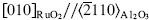
and a threefold mosaic microstructure was observed. The grain boundaries in these films were discontinuous until the substrate temperature was raised to 450 °C, where coherent grain boundaries were formed. The films grown on Al2O3 (1102) at 450 °C exhibited the epitaxial relationship: RuO2(101)//Al2O3 (1102). The in-plane alignment was RuO2〈101〉//Al2O31101〉, and the lattice parameters were the same as found in bulk RuO2. Transmission electron microscopy indicated a large degree of imperfection in the region between coalescing grains. The RuO2 films grown on SrTiO3 (100) at room temperature were amorphous. The film grown at 450 °C showed a preferential orientation with RuO2 (100)//SrTiO3 (100), but without in-plane orientation.

Type
Articles
Copyright
Copyright © Materials Research Society 1997

Access options

Get access to the full version of this content by using one of the access options below. (Log in options will check for institutional or personal access. Content may require purchase if you do not have access.)

References

1.Ryden, W. D. and Lawson, A. W., Phys. Rev. B 1, 1494 (1970).CrossRefGoogle Scholar
2.Glassford, K. M. and Chelikowski, J. R., Phys. Rev. B 49, 7107 (1994).CrossRefGoogle Scholar
3.Vadimsky, R. G., Frankenthal, R. P., and Thompson, D. E., J. Electrochem. Soc. 126, 2017 (1979).CrossRefGoogle Scholar
4.Sakiyama, K., Onishi, S., Ishihara, K., Orita, K., Kajiyama, T., Hosoda, N., and Hara, T., J. Electrochem. Soc. 140, 834 (1993).CrossRefGoogle Scholar
5.Rogers, D. B., Shannon, R. D., Sleight, A. W., and Gillson, J. L., Inorg. Chem. 8, 841 (1969).CrossRefGoogle Scholar
6.Zheng, J. P. and Jow, T. R., J. Electrochem. Soc. 142, L6 (1995).CrossRefGoogle Scholar
7.Glab, S., Hulanicki, A., Eward, G., and Ingman, F., Crit. Rev. Anal. Chem. 21, 29 (1989).CrossRefGoogle Scholar
8.Krusin-Elbaum, L. and Wittmer, M., J. Electrochem. Soc. 135, 2610 (1988).CrossRefGoogle Scholar
9.Krusin-Elbaum, L., Thin Solid Films 169, 17 (1989).CrossRefGoogle Scholar
10.Kolawa, E., Tso, F. C., Pan, E. T-S., and Nicolet, M-A., Thin Solid Films 173, 217 (1989).CrossRefGoogle Scholar
11.Charai, A., Hornstrom, S. E., Thomas, O., Fryer, P. M., and Harper, J. M. E., J. Vac. Sci. Technol. A7, 784 (1989).CrossRefGoogle Scholar
12.Takemura, K., Sakuma, T., and Miyasaka, Y., Appl. Phys. Lett. 64, 2967 (1994).CrossRefGoogle Scholar
13.Al-Shareef, H. N., Bellur, K. R., Auciello, O., and Kingon, A. I., Thin Solid Films 256, 73 (1995).CrossRefGoogle Scholar
14.Jia, Q-X. and Anderson, W. A., IEEE Trans. on Component, Hybrids, and Manuf. Technol. 15, 121 (1992).CrossRefGoogle Scholar
15.Green, M. L., Gross, M. E., Papa, L. E., Schnoes, K. J., and Brasen, D., J. Electrochem. Soc. 132, 2677 (1985).CrossRefGoogle Scholar
16.Senzaki, Y., McCormick, F. B., and Gladfelter, W. L., Chemistry of Materials 4, 747 (1992).CrossRefGoogle Scholar
17.Hones, P., Gerfin, T., and Gratzel, M., Appl. Phys. Lett. 67, 3078 (1995).CrossRefGoogle Scholar
18.Senzaki, Y., Ph.D. Thesis, University of Minnesota (1993).Google Scholar
19.Kolawa, E., So, F. C. T., Pan, E. T-S., and Nicolet, M-A., Appl. Phys. Lett. 50, 854 (1987).CrossRefGoogle Scholar
20.Al-Shareef, H. N., Auciello, O., and Kingon, A. I., in Science and Technology of Electroceramic Thin Films, edited by Auciello, O. and Waser, R. (Kluwer Academic Publishers, New York, 1994), Vol. NATO/ASI Series Vol. 284, p. 133.Google Scholar
21.Krusin-Elbaum, L., Wittmer, M., and Yee, D. S., Appl. Phys. Lett. 50, 1879 (1987).CrossRefGoogle Scholar
22.Mar, S. Y., Liang, J. S., Sun, C. Y., and Huang, Y. S., Thin Solid Films 238, 158 (1994).CrossRefGoogle Scholar
23.Jia, Q. X., Wu, X. D., Foltyn, S. R., Findikoglu, A. T., Tiwari, P., Zheng, J. P., and Jow, T. R., Appl. Phys. Lett. 67, 1677 (1995).CrossRefGoogle Scholar
24.Wang, Q., Gladfelter, W. L., Evans, D. F., Fan, Y., and Franciosi, A., J. Vac. Sci. Technol. A. 14, 747 (1996).CrossRefGoogle Scholar
25.Desu, S. B. and Yoo, I. K., Integrated Ferroelectric 3, 365 (1993).CrossRefGoogle Scholar
26.Vizkelethy, G. and Revesz, P., Surf. Interface Analysis 20, 309 (1993).CrossRefGoogle Scholar
27.Doyle, B. L. and Brice, D. K., Nucl. Instr. Methods in Phys. Res. B35, 301 (1988).CrossRefGoogle Scholar
28.van der Pauw, L. J., Philip Research Reports 13, 1 (1958).Google Scholar
29.Cameron, J. R., Phys. Rev. 90, 839 (1953).CrossRefGoogle Scholar
30.Kim, K. S. and Winograd, N., J. Catalysis 35, 66 (1974).CrossRefGoogle Scholar
31.Chen, S., Mason, M. G., Gysling, H. J., Paz-Pujalt, G. R., Blanton, T. N., Castro, T., Chen, K. M., Fictorie, C. P., Gladfelter, W. L., Franciosi, A., Cohen, P. I., and Evans, J. F., J. Vac. Sci. Technol. A11, 2419 (1993).CrossRefGoogle Scholar
32.Liu, D., Wang, Q., Chang, H. L., and Chen, H., J. Mater. Res. 10, 1516 (1995).CrossRefGoogle Scholar
33.Matthews, J. W., Epitaxial Growth B (Academic Press, New York, 1975), p. 560.Google Scholar
34.Chang, H. L. M., Zhang, T. J., Zhang, H., Guo, J., Kim, H. K., and Lam, D. J., J. Mater. Res. 8, 2634 (1993).CrossRefGoogle Scholar
35.Movchan, B. M. and Demchishin, A. V., Phys. Met. Metallogr. 28, 83 (1969).Google Scholar
36.Thornton, J. A., J. Vac. Sci. Technol. 11, 666 (1974).CrossRefGoogle Scholar