Hostname: page-component-7bb8b95d7b-l4ctd Total loading time: 0 Render date: 2024-09-08T19:27:34.298Z Has data issue: false hasContentIssue false

Growth and transport properties of p-type GaNBi alloys

Published online by Cambridge University Press:  17 November 2011

Alejandro X. Levander
Affiliation:
Materials Sciences Division, Lawrence Berkeley National Laboratory, Berkeley, California 94720; and Department of Materials Science and Engineering, University of California, Berkeley, California 94720
Sergei V. Novikov
Affiliation:
School of Physics and Astronomy, University of Nottingham, Nottingham NG7 2RD, United Kingdom
Zuzanna Liliental-Weber
Affiliation:
Materials Sciences Division, Lawrence Berkeley National Laboratory, Berkeley, California 94720
Roberto dos Reis
Affiliation:
Materials Sciences Division, Lawrence Berkeley National Laboratory, Berkeley, California 94720; and Instituto de Física, UFRGS, Porto Alegre, RS 15051, 91501-970 Brazil
Jonathan D. Denlinger
Affiliation:
Advanced Light Source, Lawrence Berkeley National Laboratory, Berkeley, California 94720
Junqiao Wu
Affiliation:
Materials Sciences Division, Lawrence Berkeley National Laboratory, Berkeley, California 94720; and Department of Materials Science and Engineering, University of California, Berkeley, California 94720
Oscar D. Dubon
Affiliation:
Materials Sciences Division, Lawrence Berkeley National Laboratory, Berkeley, California 94720; and Department of Materials Science and Engineering, University of California, Berkeley, California 94720
C.T. Foxon
Affiliation:
School of Physics and Astronomy, University of Nottingham, Nottingham NG7 2RD, United Kingdom
Kin M. Yu
Affiliation:
Materials Sciences Division, Lawrence Berkeley National Laboratory, Berkeley, California 94720
Wladek Walukiewicz*
Affiliation:
Materials Sciences Division, Lawrence Berkeley National Laboratory, Berkeley, California 94720
*
a)Address all correspondence to this author. e-mail: W_Walukiewicz@lbl.gov
Get access

Abstract

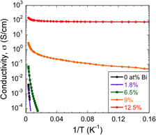
Thin films of GaNBi alloys with up to 12.5 at.% Bi were grown on sapphire using low-temperature molecular beam epitaxy. The low growth temperature and incorporation of Bi resulted in a morphology of nanocrystallites embedded in an amorphous matrix. The composition and optical absorption shift were found to depend strongly on the III:V ratio controlled by the Ga flux during growth. Increasing the incorporation of Bi resulted in an increase in conductivity of almost five orders of magnitude to 144 Ω-cm−1. Holes were determined to be the majority charge carriers indicating that the conductivity most likely results from a GaNBi-related phase. Soft x-ray emission and x-ray absorption spectroscopies were used to probe the modification of the nitrogen partial density of states due to Bi. The valence band edge was found to shift abruptly to the midgap position of GaN, whereas the conduction band edge shifted more gradually.

Type
Invited Feature Papers
Copyright
Copyright © Materials Research Society 2011

Access options

Get access to the full version of this content by using one of the access options below. (Log in options will check for institutional or personal access. Content may require purchase if you do not have access.)

References

REFERENCES

1.Walukiewicz, W., Shan, W., Yu, K.M., Ager, J.W. III, Haller, E.E., Miotkowski, I., Seong, M.J., Alawadhi, H., and Ramdas, A.K.: Interaction of localized electronic states with the conduction band: Band anticrossing in II-VI semiconductor ternaries. Phys. Rev. Lett. 85, 1552 (2000).CrossRefGoogle ScholarPubMed
2.Shan, W., Walukiewicz, W., Ager, J.W. III, Haller, E.E., Geisz, J.F., Friedman, D.J., Olson, J.M., and Kurtz, S.R.: Band anticrossing in GaInNAs alloys. Phys. Rev. Lett. 82, 1221 (1999).CrossRefGoogle Scholar
3.Alberi, K., Dubon, O.D., Walukiewicz, W., Yu, K.M., Bertulis, K., and Krotkus, A.: Valence band anticrossing in GaBixAs1-x. Appl. Phys. Lett. 91, 051909 (2007).CrossRefGoogle Scholar
4.Francoeur, S., Seong, M-J., Mascarenhas, A., Tixier, S., Adamcyk, M., and Tiedje, T.: Band gap of GaAs1-xBix, 0 < x < 3.6%. Appl. Phys. Lett. 82, 3874 (2003).CrossRefGoogle Scholar
5.Wu, J., Walukiewicz, W., Yu, K.M., Denlinger, J.D., Shan, W., Ager, J.W. III, Kimura, A., Tang, H.F., and Kuech, T.F.: Valence band hybridization in N-rich GaN1-xAsx. Phys. Rev. B 70, 115214 (2004).CrossRefGoogle Scholar
6.Bertulis, K., Krotkus, A., Aleksejenko, G., Pacebutas, V., Adomavicius, R., Molis, G., and Marcinkevicius, S.: GaBiAs: A material for optoelectronic terahertz devices. Appl. Phys. Lett. 88, 201112 (2006).CrossRefGoogle Scholar
7.Fluegel, B., Francoeur, S., Mascarenhas, A., Tixier, S., Young, E.C., and Tiedje, T.: Giant spin-orbit bowing in GaAs1-xBix. Phys. Rev. Lett. 97, 067205 (2006).CrossRefGoogle ScholarPubMed
8.Uesugi, K., Morooka, N., and Suemune, I.: Reexamination of N composition dependence of coherently grown GaNAs band gap energy with high-resolution x-ray diffraction mapping measurements. Appl. Phys. Lett. 74, 1254 (1999).CrossRefGoogle Scholar
9.Huang, W., Oe, K., Feng, G., and Yoshimoto, M.: Molecular-beam epitaxy and characteristics of GaNyAs1-x-yBix. J. Appl. Phys. 98, 053505 (2005).CrossRefGoogle Scholar
10.Novikov, S.V., Staddon, C.R., Foxon, C.T., Yu, K.M., Broesler, R., Hawkridge, M., Liliental-Weber, Z., Walukiewicz, W., Denlinger, J., and Demchenko, I.: Molecular beam epitaxy of GaNAs alloys with high As content for potential photoanode applications in hydrogen production. J. Vac. Sci. Technol. B 28, C3B12 (2010).CrossRefGoogle Scholar
11.Yu, K.M., Novikov, S.V., Broesler, R., Demchenko, I.N., Denlinger, J.D., Liliental-Weber, Z., Luckert, F., Martin, R.W., Walukiewicz, W., and Foxon, C.T.: Highly mismatch crystalline and amorphous GaN1-xAsx alloys in the whole composition range. J. Appl. Phys. 106, 103709 (2009).CrossRefGoogle Scholar
12.Yu, K.M., Novikov, S.V., Broesler, R., Liliental-Weber, Z., Levander, A.X., Kao, V.M., Dubon, O.D., Wu, J., Walukiewicz, W., and Foxon, C.T.: Low gap amorphous GaN1-xAsx alloys grown on glass substrates. Appl. Phys. Lett. 97, 101906 (2010).CrossRefGoogle Scholar
13.Foxon, C.T., Novikov, S.V., Li, T., Campion, R.P., Winser, A.J., and Harrison, I.: Bismuth a new surfactant of contact for GaN films grown by molecular beam epitaxy. Phys. Status Solidi A 192, 441 (2002).3.0.CO;2-U>CrossRefGoogle Scholar
14.Gordy, W. and Orville Thomas, W.J.: Electronegativities of the elements. J. Chem. Phys. 24, 439 (1956).CrossRefGoogle Scholar
15.Morkoç, H., Strite, S., Gao, G.B., Lin, M.E., Sverdlov, B., and Burns, M.: Large-band-gap SiC, III-V nitride, and II-VI ZnSe-based semiconductor device technologies. J. Appl. Phys. 76, 1363 (1994).CrossRefGoogle Scholar
16.Trumbore, F.A., Gershenzon, M., and Thomas, D.G.: Luminescence due to the isoelectronic substitution of bismuth for phosphorous in gallium phosphide. Appl. Phys. Lett. 9, 4 (1966).CrossRefGoogle Scholar
17.Vurgaftman, I. and Meyer, J.R.: Band parameters for nitrogen-containing semiconductors. J. Appl. Phys. 94, 3675 (2003).CrossRefGoogle Scholar
18.Levander, A.X., Yu, K.M., Novikov, S.V., Tseng, A., Foxon, C.T., Dubon, O.D., Wu, J., and Walukiewicz, W.: GaN1-xBix: Extremely mismatched semiconductor alloys. Appl. Phys. Lett. 97, 141919 (2010).CrossRefGoogle Scholar
19.Stumm, P. and Drabold, D.A.: Can amorphous GaN serve as a useful electronic material? Phys. Rev. Lett. 79, 677 (1997).CrossRefGoogle Scholar
20.Mott, N.F. and Davis, E.A.: Electronic Processes in Non-crystalline Materials (Oxford University Press, USA, 1979).Google Scholar
21.Ager, J.W. III, Miller, N., Jones, R.E., Yu, K.M., Wu, J., Schaff, W.J., and Walukiewicz, W.: Mg-doped InN and InGaN—Photoluminescence, capacitance–voltage and thermopower measurements. Phys. Status Solidi B 245, 873 (2008).CrossRefGoogle Scholar
22.Oe, K. and Okamoto, H.: New semiconductor alloy GaAs1-xBix grown by metal organic vapor phase epitaxy. Jpn. J. Appl. Phys. 37, L1283 (1998).Google Scholar
23.Yoshimoto, M., Murata, S., Chayahara, A., Horino, Y., Saraie, J., and Oe, K.: Metastable GaAsBi alloy grown by molecular beam epitaxy. Jpn. J. Appl. Phys. 42, L1235 (2003).CrossRefGoogle Scholar
24.Henini, M., Ibáñez, J., Schmidbauer, M., Shafi, M., Novikov, S.V., Turyanska, L., Molina, S.I., Sales, D.L., Chisholm, M.F., and Misiewicz, J.: Molecular beam epitaxy of GaBiAs on (311)B GaAs substrates. Appl. Phys. Lett. 91, 251909 (2007).CrossRefGoogle Scholar
25.Liliental-Weber, Z., dos Reis, R., Levander, A.X., Yu, K.M., Walukiewicz, W., Novikov, S.V., and Foxon, C.T.: Structural studies of GaN1-xAsx and GaN1-xBix alloys for solar cell applications. Phys. Status Solidi C (2011, in press).Google Scholar
26.Damodara Das, V. and Soundararajan, N.: Size and temperature effects on the Seebeck coefficient of thin bismuth films. Phys. Rev. B 35, 5990 (1987).Google Scholar
27.Van de Walle, C.G. and Neugebauer, J.: First-principles calculations for defects and impurities: Applications to III-nitrides. J. Appl. Phys. 95, 3851 (2004).Google Scholar
28.Walukiewicz, W.: Intrinsic limitations to the doping of wide-gap semiconductors. Physica B 302303, 123 (2001).CrossRefGoogle Scholar
29.Duda, L.C., Stagarescu, C.B., Downes, J., Smith, K.E., Korakakis, D., Moustakas, T.D., Guo, J.H., and Nordgren, J.: Density of states, hybridization, and band-gap evolution in AlxGa1-xN. Phys. Rev. B 58, 1928 (1998).CrossRefGoogle Scholar
30.Strocov, V.N., Schmitt, T., Rubensson, J-E., Blaha, P., Paskova, T., and Nilsson, P.O.: Momentum selectivity and anisotropy effects in the nitrogen K-edge resonant inelastic x-ray scattering from GaN. Phys. Rev. B 72, 085221 (1995).Google Scholar
31.Walukiewicz, W., Alberi, K., Wu, J., Shan, W., Yu, K.M., and Ager, J.W. III: Electronic band structure of highly mismatched semiconductor alloys, in Dilute III-V Nitride Semiconductors and Material Systems: Physics and Technology, edited by Erol, A. (Springer-Verlag, Berlin, 2008), pp. 6587.CrossRefGoogle Scholar