


Introduction
To enhance the functionality of the modern wireless systems, tunable microwave devices are important to be investigated. For example, in millimeter wave systems, beamforming networks are highly demanded, and so their elements such as tunable phase shifter and amplitude tuner. In addition, tunable devices can also save a lot of space and weight, which is important, e.g. in satellite systems. Hence, for example, a filter bank, which contains several filters with different center frequencies, can be replaced by a single tunable filter, where its center frequency is adjustable.
Tuning elements can be included into a fixed microwave component in order to obtain a tunable device. Liquid crystal (LC), specifically synthesized for microwaves, is one of the promising tuning elements, which exhibits a low loss at high frequencies, typically above 10 GHz [Reference Weickhmann1].
For an LC-based tunable device, biasing network and proper sealing of LC is needed. A technical solution for these challenges can be found by using low temperature co-fired ceramic (LTCC) technology for the fabrication process. This technology employs several layers of substrate, which also supports metallizations (planar and vias), resistive lines, and cavities. Integration of LC into phase shifters have been successfully demonstrated in [Reference Strunck2,Reference Jost3] with the help of LTCC technology. Moreover, this combination of LC and LTCC is also suitable for space applications [Reference Franke4], which gives an advantage compared with the other technologies.
An LC-LTCC component, the amplitude tuner, has been proposed in [Reference Prasetiadi5]. In this paper, the work is extended to fabricate tunable substrate integrated waveguide (SIW) filters, which are proposed for the first time. The components are working at around 30 GHz. Before discussing both components, a brief introduction to LC is given in the section “Fundamentals of LC for microwave applications”. The LTCC fabrication process is explained in the section “LTCC fabrication technology”. The proposed components are discussed in the sections “LC-based amplitude tuner” and “Electrically tunable LC-based SIW filter”, for amplitude tuner and tunable filter, respectively.
Fundamentals of LC for microwave applications
LC is a state of matter between a solid crystalline and liquid. Thus, LC inherits the property from both states of material: it can flow like a liquid but has an orientational order at the same time. This orientational order comes from the rod-like LC molecules, which tend to point at a certain direction. At a small volume, this orientation can be described by the director  $\vec {n}$, a unit vector, representing the preferred orientation of the corresponding molecules.
Anisotropy is an important property of LC, which is observable in its relative permittivity and also loss tangent. When RF electric fields are applied inside the LC, they will see a relative permittivity of  $\varepsilon _{r,\parallel }$ if those fields are in the same direction as the LC directors. On the other hand, the relative permittivity would be εr,⊥ if those fields are perpendicular to the director. Since the directors are controllable, the relative permittivity experienced by those electric fields varies continuously between those extreme states. As can be seen in Fig. 1, to align the directors into a certain orientation, biasing is needed, either magnetic or electric biasing. Usually, electrical biasing is preferred, resulting in a more compact device compared with the magnetic biasing. An example of a fully electric biasing method is described in Fig. 2 [Reference Prasetiadi6], which utilized fixed voltages V 0 and tunable voltages ±V b. By varying ±V b, both extreme states can be obtained, as well as the intermediate states.
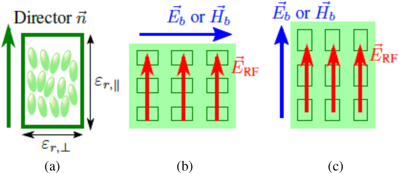
Fig. 1. The basic concepts of LC: (a) director, (b) perpendicular, and (c) parallel state of LC. The RF fields  $\vec {E}_{\rm RF}$ experience different value of permittivity, ranging from εr,⊥ to $\varepsilon _{r,\parallel }$, for perpendicular and parallel state, respectively. The states can be controlled continuously by either external electric field $\vec {E_{b}}$ or magnetic field $\vec {H_{b}}$.
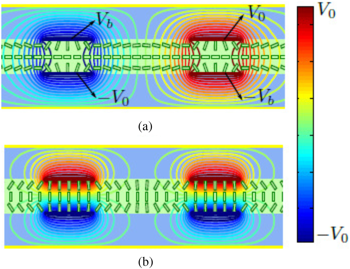
Fig. 2. An example of electrical biasing system for LC-based tunable microwave devices. Here, fixed (V 0 and −V 0) and tunable voltages (V b and −V b) are applied to the biasing lines to steer the LC director into (a) perpendicular state (when V b = −V 0) and (b) parallel state (when V b = V 0). Intermediate states can be obtained when − V 0 < V b < V 0.
The LC GT3-23001 from Merck is used and has following properties at 30 GHz: εr,⊥ = 2.47,  $\varepsilon _{r,\parallel } = $ 3.16, tan δ r,⊥ = 0.0151 and $\tan \delta _{r,\parallel } = $ 0.0033.
LTCC fabrication technology
The proposed components are fabricated by using LTCC technology, which provides an easy integration of the LC, as well as the biasing circuit, into the main components. The detailed fabrication process is explained in [Reference Jost3], where several layers of 107 μm-thick DuPont 9K7 GreenTapes were used as the LTCC substrate. This material has a relative permittivity of 7.1 and a loss tangent of 0.0015 at 30 GHz. For the metallizations, gold pastes are used, which are LL505 for the planar metallization and LL500 for the via filling. All of the biasing lines are made of a resistive paste 2061. This paste is almost transparent to the high-frequency field but it is resistive for the DC or low frequency biasing signal. All of these materials are qualified for space applications [Reference Franke4,Reference Gaebler7].
The LC cavity, which is formed through punching, occupies only a single layer of LTCC in both of the proposed components. This cavity is sealed during the fabrication process, however, a filling hole with a diameter of 0.5 mm is kept open. The LC injection, which is carried out after finishing the LTCC process, is performed through this hole in a vacuum chamber to minimize the amount of air bubbles inside the cavity. At the end, the filling hole is sealed completely by using two components glue to prevent any LC leakage.
LC-Based amplitude tuner
Amplitude-tuning devices have wide applications, for example, in RF signal cancellation circuits and complete beamforming networks. To realize such an amplitude tuner, several tuning elements can be used, for instance, tunable resistors, which can be implemented by using PIN diodes [Reference Walker8] or field-effect transistors (FET) [Reference Saavedra and Zheng9]. However, these tunable resistors need biasing currents in order to tune the resistance, leading to a nonzero power consumption. On the other hand, recent research shows that tunable capacitors or varactors can be employed to realize an amplitude tuner [Reference Trent and Weller10–Reference Cheng and Chik12]. Most of those devices are working in a low-frequency band, typically below 12 GHz. In this section, an LC-based amplitude tuner is proposed for a frequency at 30 GHz.
Operational principle of the amplitude tuner
To change the amplitude of a signal, the concept of interference in the signal theory can be employed. Let y 1 and y 2 be both time-varying sinusoidal signals with the same frequency (f), amplitude of A 1 and A 2, as well as phase of ϕ 1 and ϕ 2:
 $$\eqalign{& y_1 = A_1\cos \left( {2\pi ft + \phi _1} \right) \cr & y_2 = A_2\cos \left( {2\pi ft + \phi _2} \right).} $$
When both of the propagating signals are incident at a certain place, interference occurs. The sum of both signals is still a sinusoidal signal with the same frequency but different amplitude (A total) and phase (ϕ total):
 $$y_{\rm total} = y_1 + y_2 = A_{\rm total}\cos \left( {2\pi ft + \phi _{\rm total}} \right).$$
With the help of the phasor concept and trigonometric identities, the total amplitude and phase can be expressed as:
 $$\eqalign{& A_{\rm total} = \sqrt {A_1^2 + A_2^2 + 2A_1A_2\cos \left( {\phi _{\rm diff}} \right)} \cr & \phi _{\rm total} = \tan ^{ - 1}\left( {\displaystyle{{A_1\sin \left( {\phi _1} \right) + A_2\sin \left( {\phi _2} \right)} \over {A_1\cos \left( {\phi _1} \right) + A_2\cos \left( {\phi _2} \right)}}} \right),} $$
where ϕ diff = ϕ 2 − ϕ 1 is the phase difference between y 2 and y 1. By varying ϕ diff, the amplitude of the total signal can be controlled. For example, A total will be maximized (A total = A 1 + A 2) when ϕ diff = 0°. On the other hand, A total = 0 can be achieved when destructive interference occurs (A 1 = A 2 and ϕ diff = 180°). Therefore, continuous tuning of ϕ diff between 0° and 180° yields a continuous amplitude variation between A 1 + A 2 and 0.
Consequently, an amplitude tuner with an input signal of y(t) = Acos (2πft + ϕ) can be realized by splitting the input signal into two branches: a tunable phase shifter and a fixed transmission line. The tunable phase shifter controls the phase difference ϕ diff between both branches. The signals from both branches are combined again, yielding an output signal described by Eqn 2 and 3. An equal power divider or combiner can be employed for this purpose. In addition, DC-blocking structures are also needed to prevent the flow of the biasing current from the tunable phase shifter to the VNA. The main block diagram is shown in Fig. 3.

Fig. 3. Block diagram and working principle of the amplitude tuner. Three main subcomponents are presented: tunable phase shifter/fixed line, power divider/combiner and DC-blocking structure. The phase difference ϕ diff between the tunable phase shifter and the fixed line can be tuned continuously between 0° and 180° in order to achieve an output signal with an amplitude range of 0–A. See the signal at each point for the details.
The overall structure of the amplitude tuner, which is fabricated by using 9 layers of GreenTape, as well as the dimensions of the structure, are depicted in Fig. 4. The stripline phase shifter from [Reference Jost3] is used due to its better tunability compared with other planar LC structures, such as microstrip line. The dimensions are designed so that the tunable phase shifter exhibits a differential phase shift of 180°. For the biasing purpose, a fully electric biasing scheme is used, where voltages of  $V_\parallel $ and 0 V control the parallel state and ±V ⊥ the perpendicular state. Details of the biasing scheme are presented in [Reference Prasetiadi5]. There, simulation results from CST Microwave Studio can be seen as well, where the intended phase shift is achieved with an insertion loss <5.6 dB. For the power divider and combiner, hybrid couplers are used, due to the technological constraint on the fabrication process. The simulation results for the hybrid coupler, as well as the DC-blocking structure, are also presented in [Reference Prasetiadi5], which give additional losses of 0.6 dB for the hybrid coupler and 1 dB for the DC-blocking structure.

Fig. 4. The overall structure of the amplitude tuner with the following subcomponents: tunable LC phase shifter, fixed line, power divider/combiner (hybrid coupler), and DC-blocking structure. Nine layers of LTCC are used with a single layer thickness of h LTCC = 107 μm. The following dimensions are used: (a) l Tun = 38.3 mm, l Fix = 48 mm, w Tun = 180 μm, and w Fix = 150 μm for the tunable LC phase shifter and fixed line, (b) w line = 100 μm and w branch = 200 μm for the hybrid coupler and (c) w CPW = 150 μm, w gap = 150 μm, l Tr = 1.21 mm, w Tr = 0.96 mm, and w MS = 100 μm for the DC-blocking structure.
Measurement results
The realized device is shown in Fig. 5. In the measurement, the ports are connected to the PNA-X network analyzer from Keysight Technologies through the GSGSG probes. Three biasing pads are also shown in Fig. 5. The maximum voltages are 80 V and 100 V for  $V_\parallel $ and V ⊥, respectively.
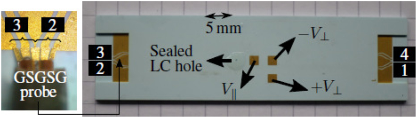
Fig. 5. Fabricated amplitude tuner. A GSGSG probe is mounted to port 1–4, as well as port 2–3. The biasing pads are connected to the voltage sources for biasing purpose.
The measurement results are compared with the simulation results of the whole structure. Both of them are presented in Fig. 6. The attenuation can be tuned continuously from 11 dB (9.5 dB in the simulation) to 30 dB with a return loss around 10 dB. The metallization is the main cause of the high insertion loss. An additional simulation (see Fig. 6c) proves that the insertion loss can be reduced to 2 dB by replacing the metallization in the device with a perfect electric conductor (PEC). On the other hand, the usage of lossless LC (LLC) with the gold paste as the metallization only reduces the insertion loss to 8 dB.
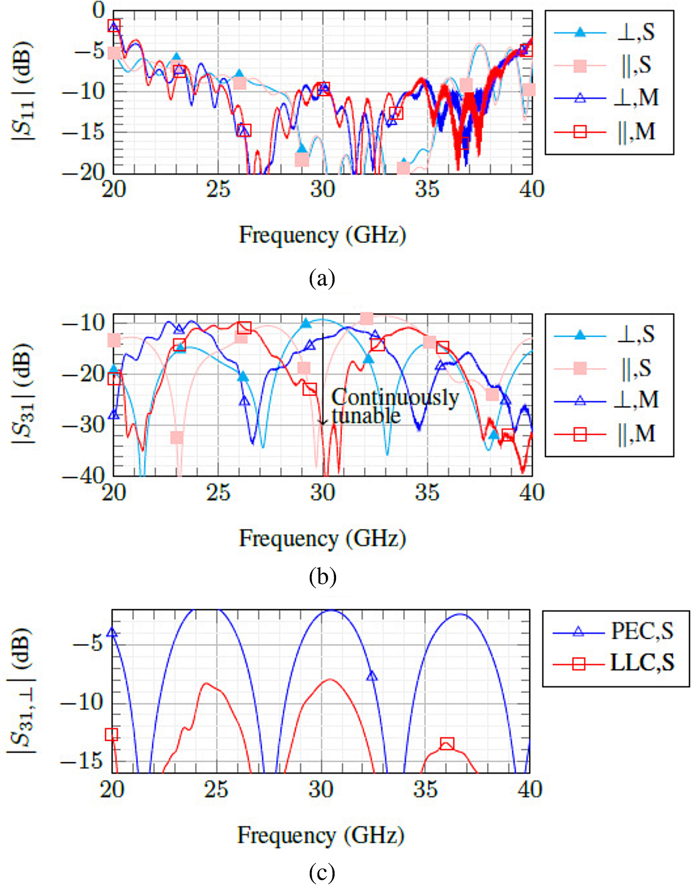
Fig. 6. Simulation and measurement results of the overall amplitude tuner structure: (a) reflection S 11 and (b) transmission coefficient S 31. Additional simulations using perfect electric conductor (PEC) and lossless LC (LLC) are also performed and included in (c). Note: S = simulation, M = measurement.
The proposed amplitude tuner is compared with other similar devices, which feature amplitude tuning properties. The comparison is summarized in Table 1. Most of them are using tunable resistors or varactors to tune the amplitude, which works at a frequency lower than 12 GHz. Although the insertion loss of this amplitude tuner with 11 dB is much higher than of the other devices, its operating frequency of 30 GHz is also much higher. In addition, the proposed component is completely space qualified, giving a major advantage compared with the existing technologies.
Table 1. Comparison of various amplitude tuners

Electrically tunable LC-based SIW filter
Several LC-based tunable bandpass filters have been reported, mostly utilizing planar structures such as periodically loaded line [Reference Goelden14], microstrip [Reference Yaghmaee15] or parallel-coupled line resonators [Reference Yazdanpanahi and Mirshekar-Syahkal16]. However, the Q-factor of the planar resonators are relatively low, typically not exceeding a Q of 40 due to system-inherently high losses of planar structures. On the other hand, waveguide structures offer tunable filters with higher Q-factors. LC-based waveguide filters have been reported [Reference Franke4], where Q-factors better than 170 around 20 GHz are obtained. However, waveguide filters are usually very bulky.
In recent years, SIW structures have attracted many researchers, due to their trade-off properties between conventional planar and waveguide structures. These structures exhibit low loss property and can be fabricated by using planar technologies, such as LTCC. Tunable SIW filters have also been fabricated using various tuning elements [Reference Zheng17–Reference Adhikari, Ghiotto and Wu20].
A magnetically tunable SIW-LC bandpass filter has been demonstrated in [Reference Prasetiadi21], resulting in a device with a Q-factor up to 105.6 operating around 20 GHz. Since the magnets consume a lot of space resulting in a bulky device, an electrically tunable SIW-LC bandpass filter is proposed in this paper. The filter will be designed to operate at 30 GHz.
Electrically tunable SIW-LC resonator
Before working on the higher order bandpass filter, a single resonator is designed first to verify the technology. An SIW cavity is designed in a 4-layer LTCC technology. The cavity structure, along with the dimensions, is depicted in Fig. 7. The dimensions are selected so that the filter will work at frequencies around 30 GHz. Inductive irises are used to couple the resonator with the SIW transmission line. The transition between the SIW line and the grounded coplanar waveguide (GCPW) line from [Reference Chen and Wu22], which is connected to the measurement probes, is also presented. In addition, the whole biasing network and the hole for LC injection are also shown in Fig. 7. Some vias are removed from the via array in the GCPW section to connect the biasing line to the biasing pad or the voltage sources.
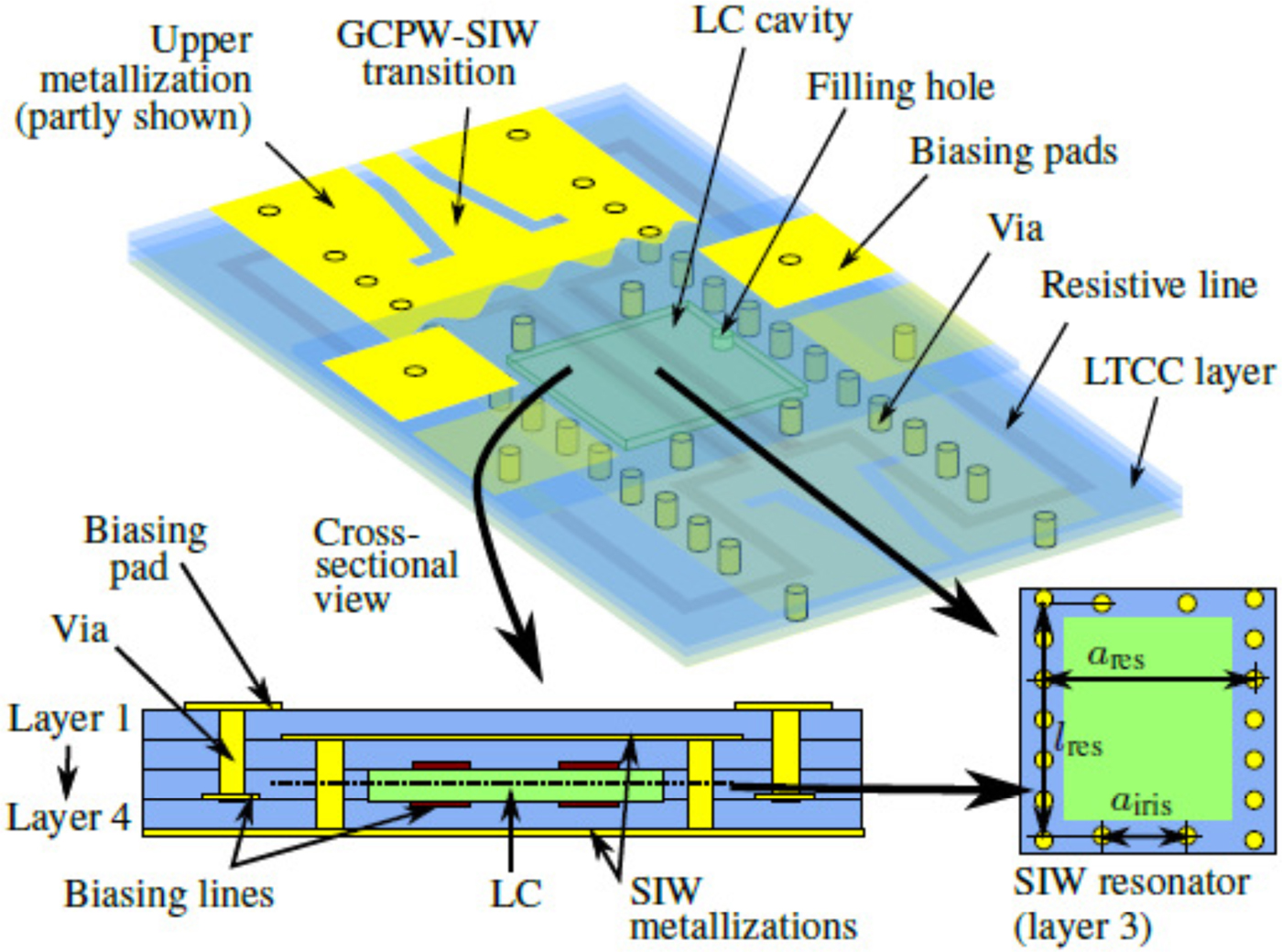
Fig. 7. LTCC-LC-based tunable SIW resonator. The following dimensions are used: a res = 3 mm, l res = 2.95 mm, a iris = 1.3 mm. The metallic via has a diameter of 0.2 mm with a pitch of 0.6 mm.
Since not all of the directors point in the same direction as indicated in Fig. 2, the effective value of relative permittivity of LC εr,eff will be examined first by using a simulation tool SimLCwg from [Reference Gaebler23]. A transmission line, which its cross section is the same as the resonator's cross section, is utilized. Fig. 8 shows the relation of the propagation constant β of the aforementioned structure and the effective relative permittivity of LC. The effective relative permittivity is obtained for LC GT3-23001 in this SIW structure: εr,eff, ⊥ = 2.64 and  $\varepsilon _{r,{\rm eff},\,\parallel } =$ 3.1. These values will be employed in the simulation of the resonator.
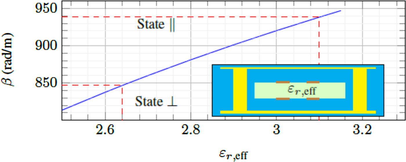
Fig. 8. The effective permittivity of LC for the proposed resonator structure.
Using CST Microwave Studio, this structure is simulated and the center frequency varies from 31.4 GHz at perpendicular state to 30.3 GHz at parallel state (tunability of 4% or 1100 MHz) as can be seen in Fig. 9. The obtained Q-factors are 69 for the perpendicular state and 118 for the parallel state. Note that the parallel state always has the better Q-factor due to its lower loss tangent.
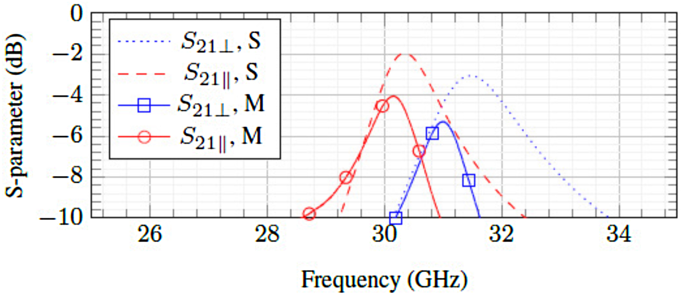
Fig. 9. Simulation (S) and measurement (M) results for an LC-SIW resonator.
The resonator, which is fabricated at the German Federal Institute for Materials Research and Testing, is shown in Fig. 10. After the fabrication process, measurements can be performed. The biasing scheme is the same as in Fig. 2, where voltages of V 0, −V 0, V b and −V b are applied to each biasing pad. The S-parameter measurement results are also depicted in Fig. 9. The tuning range is reduced to 30.16 GHz to 31 GHz (tuning of 3% or 840 MHz), possibly due to the fabrication tolerance. The Q-factors are 68–100. To achieve the extreme states, the maximum voltage needed is 80 V both for V 0 and V b.
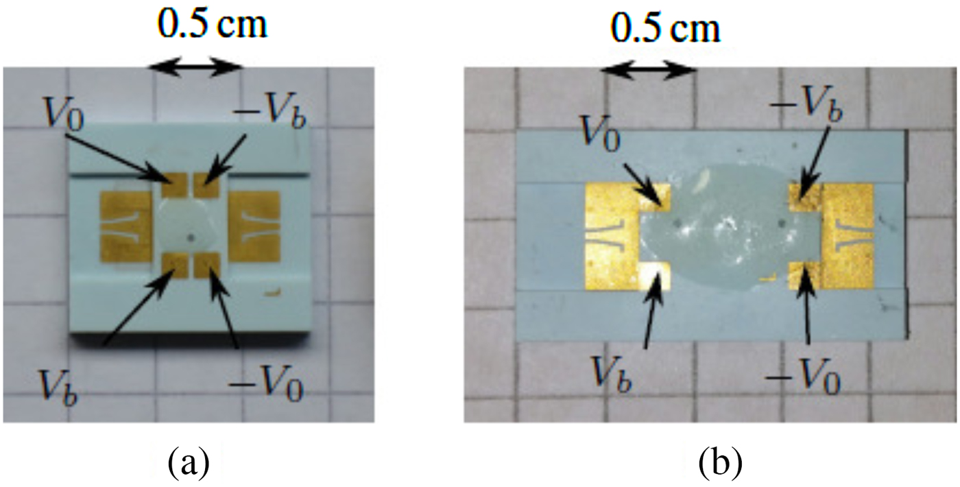
Fig. 10. Fabricated tunable SIW devices: (a) resonator and (b) filter. The configuration of the biasing voltage is also shown.
In addition to the S-parameters, the tuning time of this resonator is also investigated. For this purpose, continuous wave measurements at a single frequency are performed, which provide a better recording speed compared with the measurement for whole frequency range. The phases, which correspond to the LC state, are measured at 30.5 GHz. The tuning times are measured between 10 and 90% of the phase shift. The obtained tuning time is 2 s and 1.5 s, as shown in Fig. 11, for rise and fall time, respectively. This is a major improvement compared with the LC-based waveguide filter, which has tuning times in order of minutes [Reference Franke4].
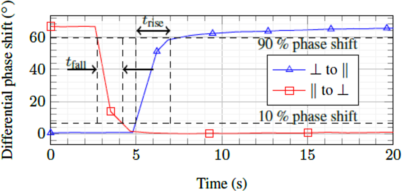
Fig. 11. The tuning time measurement of the SIW resonator, which is conducted through the differential phase shift measurement at 30.5 GHz.
Electrically tunable SIW-LC 3-pole bandpass filter
The SIW-LC resonators can be cascaded to form a higher order bandpass filter. Designed for the center frequency of 30 GHz, the structure depicted in Fig. 12 is simulated using CST Microwave Studio. This filter is a 3-pole Chebyshev filter designed for a 3 GHz ripple bandwidth. As shown in Fig. 13, the simulation yields a center frequency tuning range of 29.4–30.2 GHz while the measurement gives almost similar results, 29.4–30.1 GHz, i.e. a tuning range of 700 MHz. The difference can be seen on the return loss, which is reduced to 6 dB due to imperfect transition at the input/output ports. The filter has an insertion loss from 2 dB at the parallel state and up to 4 dB at the perpendicular state with a ripple up to 3 dB. The fractional ripple bandwidth for both states has a small difference: 11.6% at perpendicular and 11.2% at parallel state.
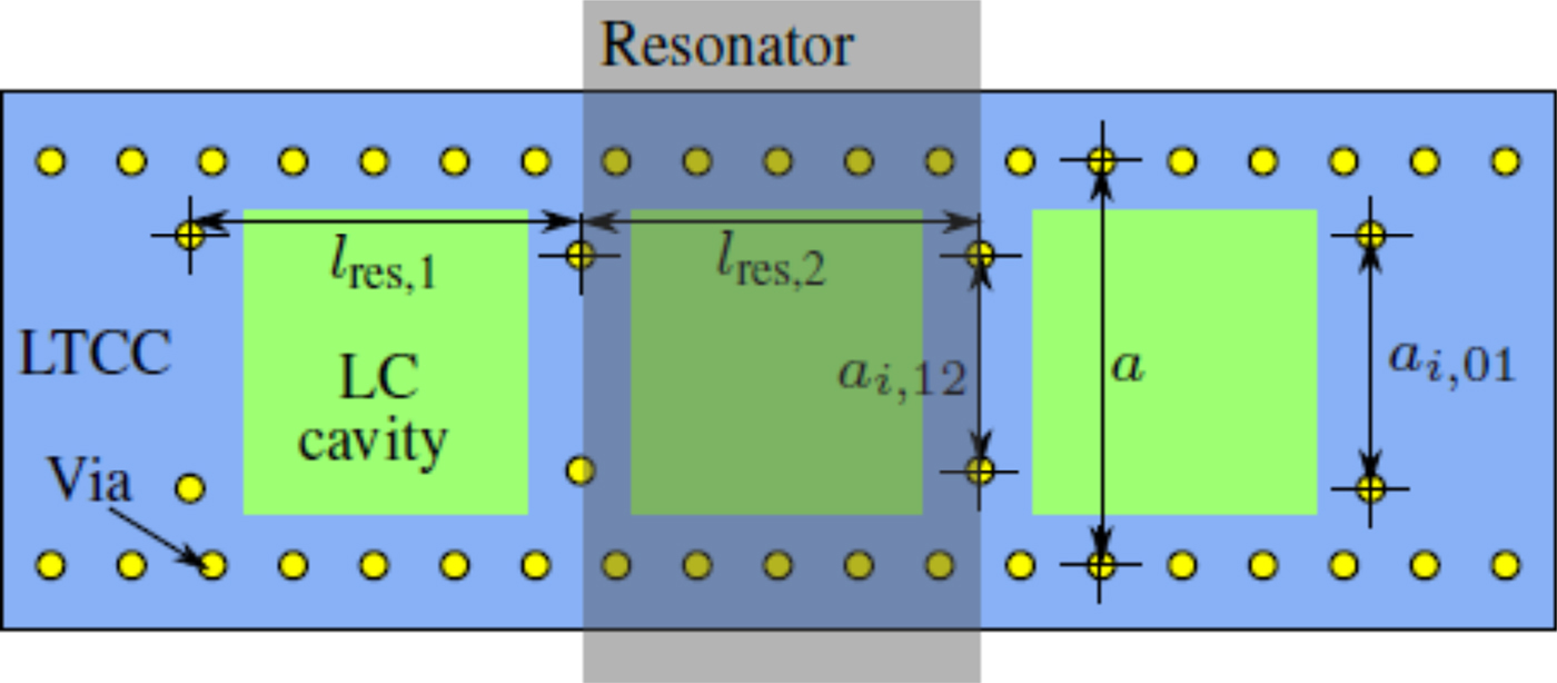
Fig. 12. 3-pole tunable Chebyshev filter using LTCC. The following dimensions are used: l res, 1 = 2.89 mm, l res, 1 = 2.95 mm, a i,01 = 1.89 mm, a i,12 = 1.6 mm, and a = 3 mm. Note that the structure is symmetric.
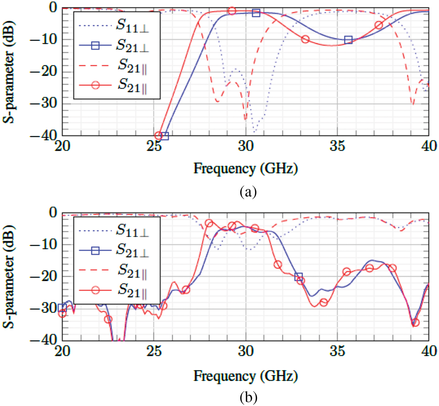
Fig. 13. The (a) simulation and (b) measurement results of the 3-pole filter.
The comparison of this filter and other proposed filter is presented in Table 2. It can be seen that the Q-factors of the SIW filter are higher compared with planar LC-based filters, which yield Q-factors typically below 40. Although waveguide filters [Reference Franke4] are expected to have a better Q-factor, its size and weight are drawbacks. Compared with the other tuning elements, the operating frequency of this filter is generally much higher with comparable Q-factors, which makes this LC filter more promising.
Table 2. Comparison of tunable resonators and filters with various tuning technology

n, filter order; f 0, center frequency; IL, insertion loss; and FBW, fractional bandwidth.
Conclusion
In this paper, two tunable microwave components have been demonstrated and fabricated by using LTCC technology: amplitude tuner and tunable filters. The amplitude tuner employs a tunable-LC phase shifter in stripline topology. Based on the interference principle, the output amplitude can be continuously controlled by changing the biasing voltage at the tunable phase shifter. The measurement results exhibit an attenuation range of 11–30 dB at 30 GHz, which has a suitable agreement with the simulation.
The second device, which is the tunable filter, is designed in SIW topology due to its low loss property. First, a resonator has been fabricated to verify the idea. It has Q-factors in the range of 68–100 with a tuning range of 840 MHz. This resonator can be combined to make a higher order filter, for example 3-pole Chebyshev filter, which works around 30 GHz. This filter has also been demonstrated with a tuning range of 700 MHz and ripple bandwidth around 11%.
Acknowledgments
This work was supported by DLR (German Space Agency), research grant no. FKZ 50 YB 1316 (Liquida K). The authors also thank to CST AG and Merck KGaA, for the simulation software and LC-mixtures, respectively.
 Ananto Eka Prasetiadi received a bachelor and master degree in telecommunication engineering from the Institut Teknologi Bandung, Bandung, Indonesia in 2010 and 2011, respectively. Since 2012, he is pursuing a Ph.D. degree at the Institute of Microwave Engineering and Photonics, Technische Universitaet Darmstadt, Darmstadt, Germany. His current main research interests are the tunable devices based on liquid crystals.
 Matthias Jost was born in Birkenfeld, Germany in 1985. He received the Dipl.-Phys. degree in experimental physics from the Johannes Gutenberg-Universitaet Mainz, Germany, in 2012. Since then, he is working towards his Ph.D. degree in the Institute of Microwave Engineering and Photonics at Technische Universitaet Darmstadt, Germany. His research is currently focussed on continuously tunable RF devices based on liquid crystal technology for satellite communication.
 Baerbel Schulz received the diploma degree in materials engineering from the University of Architecture and Building in Weimar, Germany, in 1982. From 1982 to 1991 she worked as research assistant in the field metal/ceramic packages at the factory for television electronics in Berlin, Germany. Since 1993 she is a research assistant at the Federal Institute for Materials Research and Testing in Berlin, where she works on the production of laminated composites in LTCC multilayer technology and the material parameter identification. In various projects ceramic multilayer modules were developed for LTCC-applications.
 Matthias Quibeldey was born in Recklinghausen, Germany, in 1982. He received his Diploma in electrical engineering from the University of Duisburg-Essen, Germany, in 2008. Since then, he is working at the IMST GmbH in Kamp-Lintfort, Germany. As a member of the department RF components, his research is currently focused on the design of mixed-signal devices.
 Torsten Rabe was born in Fuerstenberg, Germany, in 1957. He received the Dipl.-Ing. and PhD in material science at Bauhaus University in Weimar/Germany, in 1980 and 1983, respectively. In 1983 he joined division Ceramic Materials at Academy of Sciences in Berlin. Since 1991 he is working at the German Federal Institute for Materials Research and Testing (BAM) in Berlin and since 2012 he is head of the division Advanced Technical Ceramics. His research focuses on material development (LTCC, HTCC, reference materials), tape casting, multilayer technology, brazing of ceramic materials and non-destructive testing of green and sintered ceramic components. He is author and co-author of more than 150 publications.
 Ruediger Follmann was born in Pruem, Germany in 1968. He received Dipl.-Ing. From RWTH Aachen in 1995 and Dr.-Ing. from Duisburg University in 1998, both Germany. Since 1995 R. Follmann has been working with IMST GmbH, Germany. At IMST he was responsible for RF measurements and modeling techniques, integrated circuit and PCB design as well as for RF components. In 2016 R. Follmann became Vice President of IMST, where he is currently heading the department RF circuits and system integration. His main research topics are integrated mm-wave systems and circuits, solid-state radar systems, and new materials. R. Follmann is the author of more than 80 publications and two books. He is the inventor of two patents and member of the editorial board of FREQUENZ, DeGruyter.
 Rolf Jakoby was born in Kinheim, Germany, in 1958. He received the Dipl.-Ing. and Dr.-Ing. Degrees in electrical engineering from the University of Siegen, Germany, in 1985 and 1990, respectively. In 1991, he joined the Research Center of Deutsche Telekom in Darmstadt, Germany. Since 1997 he has been a Full Professor at TU Darmstadt. He is a co-founder of ALCAN Systems GmbH, author of more than 320 publications and holds 20 patents. His interdisciplinary research focuses on tunable passive microwave devices, beam-steering antennas, chipless RFID tags and wireless sensors, using metamaterial, ferroelectric and liquid crystal technologies. Rolf Jakoby received an award from CCI Siegen for his excellent Ph.D. in 1992 and the ITG-Prize in 1997 for an excellent publication in the IEEE AP Transactions. His group received 19 awards and prizes for best papers and doctoral dissertations. He is editor-in-chief of FREQUENZ, DeGruyter, member of VDE/ITG and of the IEEE/MTT/AP society. He was Chairman of the EuMC in 2007 and GeMiC in 2011 and is Treasurer of the EuMW in 2013 and 2017.


