


Introduction
A 140-GHz band or D-band (110–170 GHz) has been utilized for many applications by the Federal Communications Commission such as radio astronomy, satellite communications, and industry, scientific and medical (ISM) band (around 122 GHz) applications. For future high-rate wireless communications, the D-band is very promising among terahertz frequency bands. So far, several long-range D-band wireless communication systems have been successfully demonstrated [Reference Hirata, Kosugi, Takahashi, Yamaguchi, Nakajima, Furuta, Ito, Sugahara, Sato and Nagatsuma1, Reference Wang, Lin, Chen, Lu, Deng and Zhang2]. Traditional high-gain Cassegrain antennas are utilized to compensate the high propagation loss in these systems. However, this kind of antenna is bulky and not suitable for highly integrated systems.
In recent years, new types of high-gain antennas with low-profile properties are emerging [Reference Kim, Hirokawa, Ando, Takeuchi and Hirata3–Reference Miao, Hao, Luo, Gao, Wang, Wang and Hong6] in the D-band driven from high-gain and high-integration requirements. Diffusion bonding technology is using several thin metal layers to construct hollow waveguide and radiating structures which shows high radiation efficiency. A 32 × 32-element array shows more than a 38 dBi gain with over 60% efficiency and a 64 × 64-element array shows more than a 43 dBi gain with over 50% efficiency [Reference Kim, Hirokawa, Ando, Takeuchi and Hirata3]. Substrate integrated waveguide (SIW) uses via holes to construct a dielectric filled waveguide-like transmission line and electromagnetic wave can be confined in SIW by properly choosing the via diameter and spacing [Reference Uchimura, Takenoshita and Fujii7]. SIW can be easily implemented using low temperature co-fired ceramic (LTCC) technology which can be traced back to 1980s [Reference Harper and Sampson8]. In the last two decades, antennas based on LTCC technology received much researchers’ attention [Reference El-Tager, Bray and Roy9–Reference Yang, Wang, Che, Huang and Wang12] promoted by the SIW structure. To date, LTCC technology is more mature than diffusion bonding technology and shows great vitality. However, the relatively high permittivity of LTCC will constrain the energy and reduce antenna gain. Several solutions have been used in literature to solve this problem. Open air cavities have been introduced in array design in [Reference Yeap, Chen and Qing13], resulting in a 1–2 dB gain enhancement. In [Reference McKinzie, Nair, Thrasher, Smith, Hughes and Parisi14], electromagnetic band-gap (EBG) structure have been used to suppress surface waves yielding a 4-dB gain enhancement. However, EBG structure requires a large area to achieve its performance.
In this paper we firstly proposed a cavity backed patch antenna element using LTCC technology at 140 GHz. Substrate integrated cavity (SIC) is introduced to suppress surface waves and improve the gain performance. Furthermore, a rectangular ring is introduced around the patch for better impedance matching. Based on the high-gain antenna element, a 4 × 4 element array and an 8 × 8-element array are presented afterward. Finally, the comparison of simulated and measured results of the two arrays are shown.
Antenna configuration
Figure 1 shows the layer configuration of the proposed LTCC antennas. The antennas are constructed by eight substrate layers and five metal layers. The thicknesses of each substrate layer and metal layer are 0.096 and 0.01 mm, respectively. Ferro A6M is used as the substrate material with a permittivity of 5.9 and a loss tangent of 0.002. Metals are set to silver with a conductivity of 6.1 × 10⁷S/m. All the simulations in this paper are taken in the full-wave simulation software Ansys HFSS.
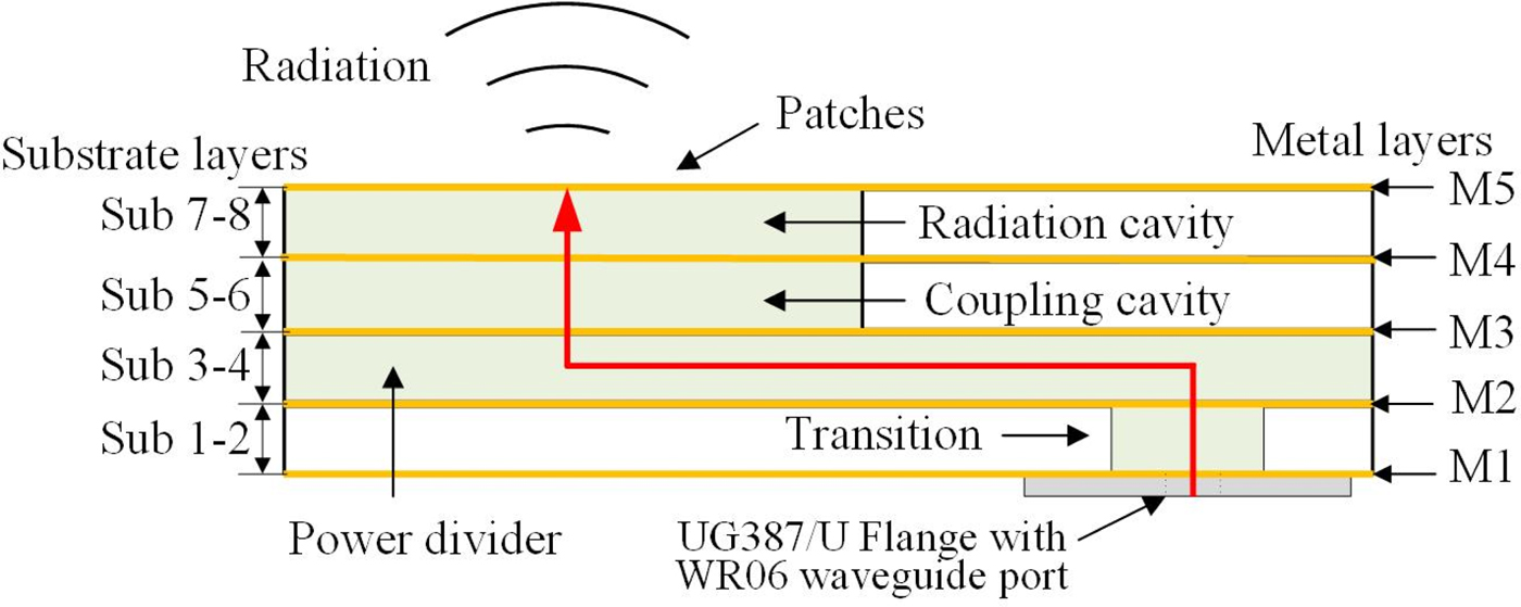
Fig. 1. Layer configuration of the proposed arrays in LTCC.
Element design
An exploded view of the proposed element antenna model built in HFSS is given in Fig. 2(a). The element only uses Sub 3–8 substrate layers and M2-5 metal layers. A rectangular patch is placed on M5 layer with a rectangular ring loaded around it. A slot is etched on M4 metal layer to excite the radiation patch. The energy is fed by an aperture etched on M3. A SIC is constructed in Sub 5–6 layer for gain enhancement. Two reference antennas are also given in Fig. 2(a) for comparison. Antenna 1 is an antenna with only a patch on M5 layer. As compare to antenna 1, a SIC around the patch is added in antenna 2. Detailed dimensions of the proposed antenna element in Fig. 2(b) can be found in Table 1. All the three antennas are with the same total size of 2 mm × 2.5 mm.
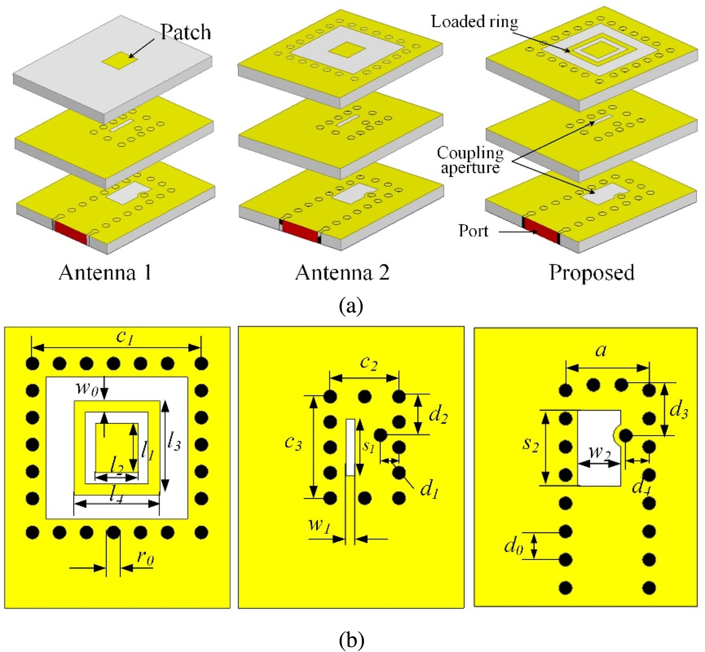
Fig. 2. Array element. (a) Exploded view of the models in HFSS (antenna 1, antenna 2, and the proposed antenna element). (b) Dimensions of the proposed antenna element.
Table 1. Dimensions of the proposed antenna element (unit: mm).

Figure 3 shows the simulated results of the three antennas. Considering array design, we should keep the refection coefficient of an antenna element below −15 dB. Antenna 1 shows a narrow −15 dB bandwidth with the lowest gain of 6 dBi among these three antennas. This is mainly caused by surface waves due to the high permittivity. Surface waves are prevented by using the SIC [Reference Tian Yang, Wei and Yan15–Reference Luo, Hu, Liang, Yu and Sun16], hence the maximum gain of antenna 2 is improved to about 9.3 dBi. However, antenna 2 shows a poor impedance matching. By introducing a rectangular ring, the proposed antenna gives a −15 dB bandwidth of 8.4 GHz (135.9–144.3 GHz). The ring loading shifts down the upper resonant frequency from 149.3 to 142.5 GHz and improves the impedance performance. On the other hand, the ring loading is also a radiating component which has the same current direction with the center patch. Thus, the maximum gain is further improved to 9.8 dBi at 145 GHz.
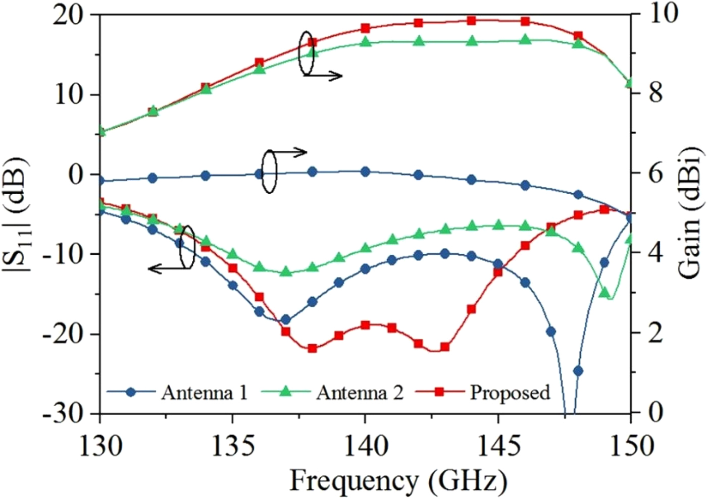
Fig. 3. Simulated |S 11| and gains of the three antenna elements.
Arrays configuration
Two antenna arrays are built with a scale of 4 × 4 and 8 × 8 based on the proposed high-gain element antenna. Figs 4(a)–4(b) gives two explosion views of the arrays, respectively. Figures 4(c)–4(e) gives three top views of the radiation part of the 8 × 8-element array. These parts of the 4 × 4-element array are a quarter that of the 8 × 8-element array which are not shown here. WR-06 waveguide with UG-387 flange is used in both arrays to feed the energy. Figure 4(f) shows the transition part from WR-06 to the SIW feeding network. As shown in Fig. 4(e), some adjacent SIWs are sharing one via holes wall resulting in a compact feeding network [Reference Chu, Li, Xiao, Qi and Huang17]. The radiation elements are spaced with 1.5 mm (0.7- wavelength at 140 GHz) intervals and they are fed with equal phase and amplitude by the feeding network.

Fig. 4. Views of the 4 × 4-element array and the 8 × 8-element array. (a) Exploded view of the 4 × 4-element array; (b) exploded view of the 8 × 8-element array. (c) Top view of M5 and via holes in Sub 7–8. (d) Top view of M4 and via holes in Sub 5–6. (e) Top view of M3 and via holes in Sub 3–4. (f) WR-06 to SIW transition.
Results and discussions
The proposed 4 × 4-element and 8 × 8-element antenna arrays were fabricated by LTCC process. Photographs of the fabricated prototypes are shown in Fig. 5. The overall dimensions of the 4 × 4-element array and the 8 × 8-element array are 20 mm × 35 mm and 18.2 mm × 33.15 mm, respectively. Actually, the overall size of the two arrays is designed in the same dimensions. However, due to the fabrication area limitation, there is a little change in the 8 × 8-element array which does not effect on the array performance.
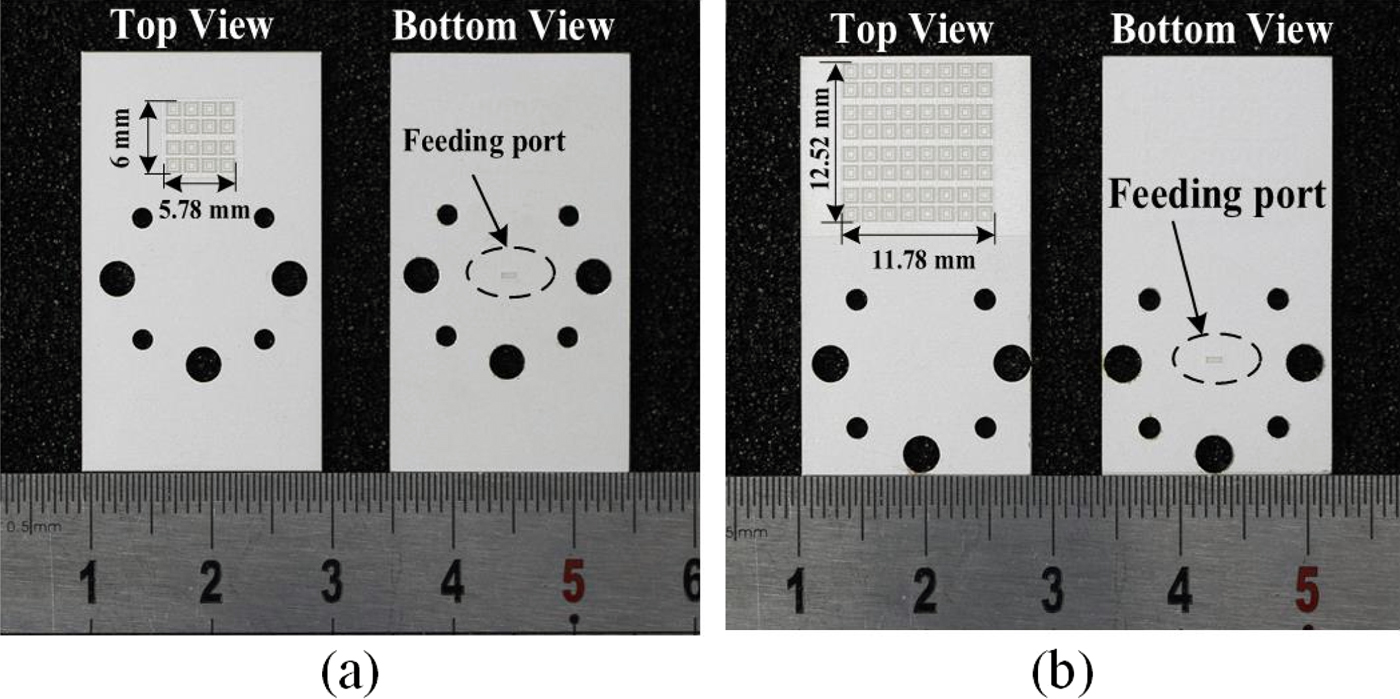
Fig. 5. Fabricated antenna arrays. (a) 4 × 4-element array. (b) 8 × 8-element array.
The impedance matching performance of the proposed antennas was measured by Ceyear AV3672B vector network analyzer with frequency extension module AV3646A. The radiation characteristics were measured in an anechoic chamber with a far-field measurement system (As shown in Fig. 6). The simulated and measured reflection coefficients are compared in Fig. 7. The simulated −8 dB bandwidth of the 4 × 4-element array is 9.5 GHz (135.8–145.3 GHz) while the measured bandwidth is 9.5 GHz(136.2–145.7 GHz). The simulated −8 dB bandwidth of the 8 × 8-element array is 9.4 GHz (136.2–145.6 GHz) while the measured bandwidth is 9.8 GHz (136.7–146.5 GHz). The measured |S11| shows more ripples and larger reflection than the simulated ones, this may be due to some fabrication errors.

Fig. 6. Measurement setup.
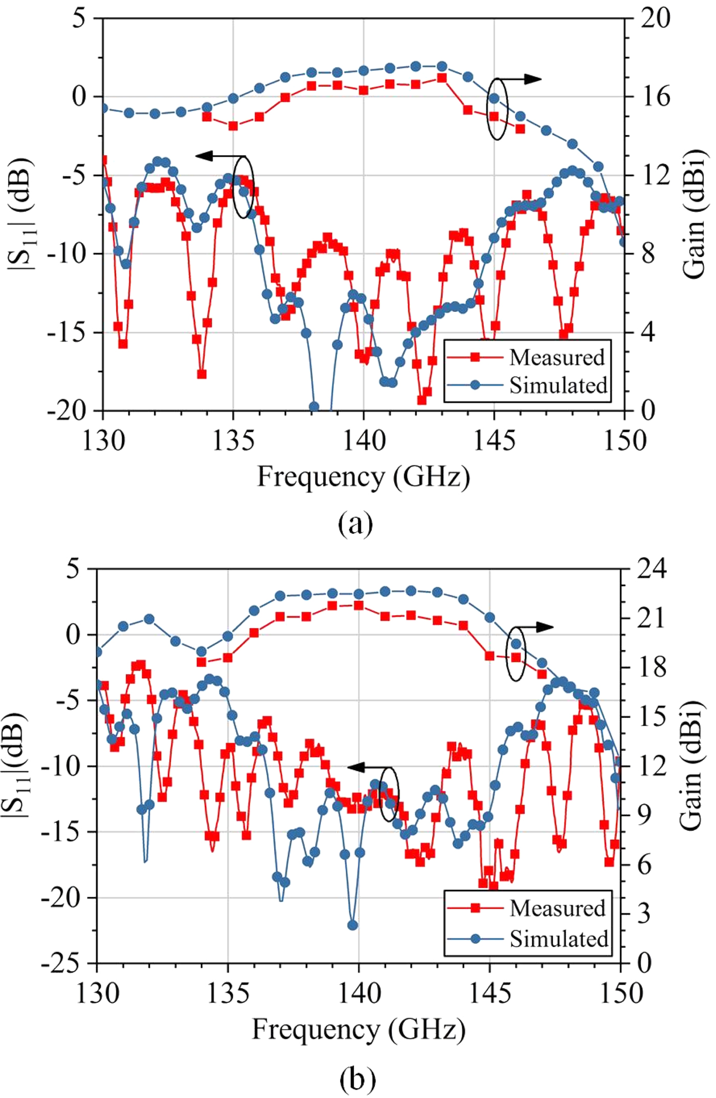
Fig. 7. Simulated and measured |S 11| and gains. (a) 4 × 4-element array. (b) 8 × 8-element array.
The simulated and measured gains are also compared in Fig. 7. For the 4 × 4-element array, the maximum simulated gain is 17.5 dBi at143 GHz, while the measured maximum gain is 16.9 dBi at 143 GHz. For the 8 × 8-element array, the maximum simulated gain is 22.7 dBi at 142 GHz, while the measured maximum gain is 21.8 dBi at 140 GHz. The simulated gains of the 4 × 4-element array and 8 × 8-element array at 140 GHz are 17.5 and 22.7 dBi with radiation efficiency of 60.8 and 47.2%, respectively. The measured gain of the 4 × 4-element array at 140 GHz is 16.3 dBi. The measured radiation efficiencies can be calculated by comparing the simulated directivity and the measured gains. It can be estimated that the measured efficiencies are 46.1 and 38.3% at 140 GHz for the 4 × 4- and 8 × 8-element array, respectively.
The simulated and measured normalized radiation patterns in the E-plane and the H-plane of the two antennas are shown in Figs 8(a)–8(b). In most cases, the measured beam patterns match well with the simulated ones and the cross polarizations stay at almost the same level of the simulated ones in both the E-plane and the H-plane for both arrays. However, there exist some differences in the side lobe level of the 144-GHz H-plane for both arrays. In such high frequencies, this is primarily because of the feeding setup near the antenna in measurement.

Fig. 8. Simulated and measured radiation patterns in the E-plane and the H-plane at 136, 140, and 144 GHz. (a) 4 × 4-element array. (b) 8 × 8-element array.
The characteristics and performances of the proposed arrays and other published 140 GHz LTCC antenna arrays are listed in Table 2 for comparison. As compared to [Reference Xu, Chen, Qing and Hong5], the proposed 4 × 4-element array gives a higher gain for the same scale. As compared to [Reference Xu, Chen, Qing and Hong18], the proposed 8 × 8-element array gives a higher gain and higher radiation efficiency. The proposed arrays merit high gain property and are suitable for 140 GHz wireless communications.
Table 2. Comparison with other published 140-GHz LTCC antenna arrays

a |S 11|≤ −5 dB.
b simulated.
Conclusion
This paper proposed a 4 × 4-element and an 8 × 8-element cavity backed patch antenna array at 140 GHz based on LTCC technology. By introducing a SIC and a rectangular ring load to the antenna element, a high gain of 9.8 dBi is achieved. Measured results show that the 4 × 4-element array possesses 9.5-GHz bandwidth (136.2–145.7 GHz) with a maximum gain of 16.9 dBi and the 8 × 8-element array possesses 9.8-GHz bandwidth (136.7–146.5 GHz) with a maximum gain of 21.7 dBi. In general, the proposed antennas have the potential to be used for 140 GHz wireless communications.
Acknowledgement
This work is supported in part by the project 61601050 from the National Natural Science Foundation of China (NSFC), in part by the National Key Research and Development Program of China (No. 2018YFF0212102), in part by the pre-research project 6140518040116DZ02001 from the Equipment Development Department of the Central Military Commission of China, and in part by BUPT Excellent Ph.D. Students Foundation.
 Zihang Qi, received B.Eng. degree in 2013. He is currently pursuing the Ph.D. degree with the Beijing University of Posts and Telecommunications. His current research interests include millimeter-wave/THz antennas and microwave filters.
 Xiuping Li, received the B.S. degree from Shandong University in 1996, the Ph.D. degree from Beijing Institute of Technology in 2001. From 2001 to 2003, she joined in Positioning and Wireless Technology Center, Nanyang Technological University in Singapore, where she was a research fellow and involved in the research and development of RFID system. In 2003, she was a research professor in Yonsei University, Seoul, South Korea. Since 2004, she joined Beijing University of Posts and Telecommunications as an associate professor, and promoted to professor in 2009. She is currently the vice dean of School of Electronic Engineering, Beijing University of Posts and Telecommunications, Beijing, China.
She has been selected into the New Century Excellent Talents Support Plan in National Ministry of Education, Beijing Science & Technology Nova Support Plan, in 2007 and 2008, respectively. She won the second prize of progress in science and technology, Chinese Institute of Communications in 2015. She was the recipient of the awards of Distinguished Youth Teacher of Beijing in 2017, Excellent Teacher of Beijing in 2017. She is the author of four books, over 100 journal and conference papers. She is also awarded more than 20 PRC patents. Her current research interests include millimeter-wave antennas, THz antennas, RFID systems, and MMIC design.
 Jinjin Chu, received the master degree from Beijing University of Posts and Telecommunications in 2017. She is currently working at Huawei company.
 Jun Xiao received the B.Eng. degree and the M.Eng. degree from Harbin Institute of Technology, Harbin, China, in 2008 and 2011, respectively. He is currently working toward the Ph.D. degree in electronic science and technology at the Beijing University of Posts and Telecommunications, Beijing, China. His research interests include UWB antennas, millimeter-wave antennas and THz antennas.
 Hua Zhu, received the M.S. degree from Guilin University of Electronic Technology, Guilin, China, in 2010, and the Ph.D. degree from Beijing University of Posts and Telecommunications, Beijing, China, in 2015. She is currently a lecturer of Beijing University of Posts and Telecommunications, Beijing, China. Her research interests include UHF RFID beam scanning antenna array design in complex environment and millimeter wave/Terahertz antenna design.


