


Introduction
The field of industrial measurement systems was dominated by conventional measurement systems like mechanical, ultrasonic, laser, or x-ray-based sensors for decades. For a wide range of highly specialized measurement scenarios commonly used in modern industrial processes, those measurement systems suffer from fundamental problems. Mechanical sensors like floating switches require a high amount of maintenance, contactless ultrasonic sensors don't work under vacuum conditions and need typically a coupling liquid, laser-based sensor systems are sensitive to harsh environmental conditions like steam or dirt, and x-ray-based sensor systems require a high amount of safety precautions and housing due to ionizing radiation and are very expensive.
To overcome these drawbacks, modern radar-based sensor systems are gaining more and more relevance in the field of industrial measurement applications. Thus, radar-based sensors are already used for tank-level probing radar [Reference Vogt and Gerding1, Reference Brumbi2], non-destructive testing [Reference Peichl, Albers and Dill3, Reference Clavero, Solano, Silla, Schröder and Schössele4], material characterization for recycling plastics [Reference Nuessler, Pohl, Kuels, Hein and Stein5], micromachining [Reference Ayhan, Thomas, Kong, Scherr, Pauli, Jaeschke, Wulfsberg, Pohl and Zwick6], blast furnace monitoring [Reference Chen, Liu, Hou and Lu7], or even security applications [Reference Macfarlane, Robertson and Bryllert8, Reference Robertson, Macfarlane and Bryllert9]. To fulfill the requirements of these modern industrial and security applications, a high range resolution and a high measurement accuracy combined with compact sensor dimensions are inevitable. To achieve those demands, the use of high measurement frequencies above 200 GHz is beneficiary, as higher frequencies allow a larger modulation bandwidth and, especially with the use of integrated sensor concepts, a smaller sensor size. As the frequency range above 200 GHz was dominated by III–V semiconductor technologies several years ago, these technologies suffer from a limited integration density and quite expensive manufacturing costs. In contrast, the development of modern Silicon-Germanium (SiGe) technologies during the last several years, enables the combination of high output frequencies above 200 GHz, a high integration density, and a cost-effective, industrial grade, high volume production [Reference Božanić and Sinha10].
A commonly used system concept to generate output frequencies above 200 GHz with SiGe-based monolithic microwave integrated circuits (MMIC) is to use a local oscillator at a lower fundamental frequency with subsequent frequency multiplication. Here, the isolation of the fundamental signal is limited by the frequency multiplier, resulting in parasitic radiation. In frequency modulated continuous wave (FMCW) radar operation, this parasitic signal leads to a false target, which appears at half the distance of the original target. This results in an ambiguous measurement, unable to determine if the target at half the distance is a second real target or the result of the parasitic measurement. This ambiguousness might be a problem for several measurement scenarios.
To suppress the parasitic signal, a filter structure based on an interference filter was developed and integrated into the body of the dielectric lens of an ultra-compact radar sensor to demonstrate the filter capabilities of the structure. To fabricate the lens prototypes, a conventional milled lens was manufactured, made from polytetrafluoroethylene (PTFE), and compared with prototypes built by additive manufacturing through selective laser sintering (SLS) and stereolithography (SLA).
An earlier version of this paper was presented at the 2021 IEEE 51st European Microwave Conference (EuMC) and was published in its proceedings [Reference Thomas, Shoykhetbrod and Pohl11]. This paper extends the earlier version by additionally introducing a milled PTFE lens in comparison to the additive manufactured lens in terms of filter performance and material losses, as well as a more detailed analysis of several effects affecting the filtering performance and side lobe behavior of the filtering structure.
Used radar sensor
The radar sensor used for demonstrating the impact of parasitic fundamental feed-through signals and to prove the filtering lens antenna concept is shown in Fig. 1. Core of the sensor is a in-house developed SiGe transceiver MMIC depicted in the upper corner of Fig. 1.
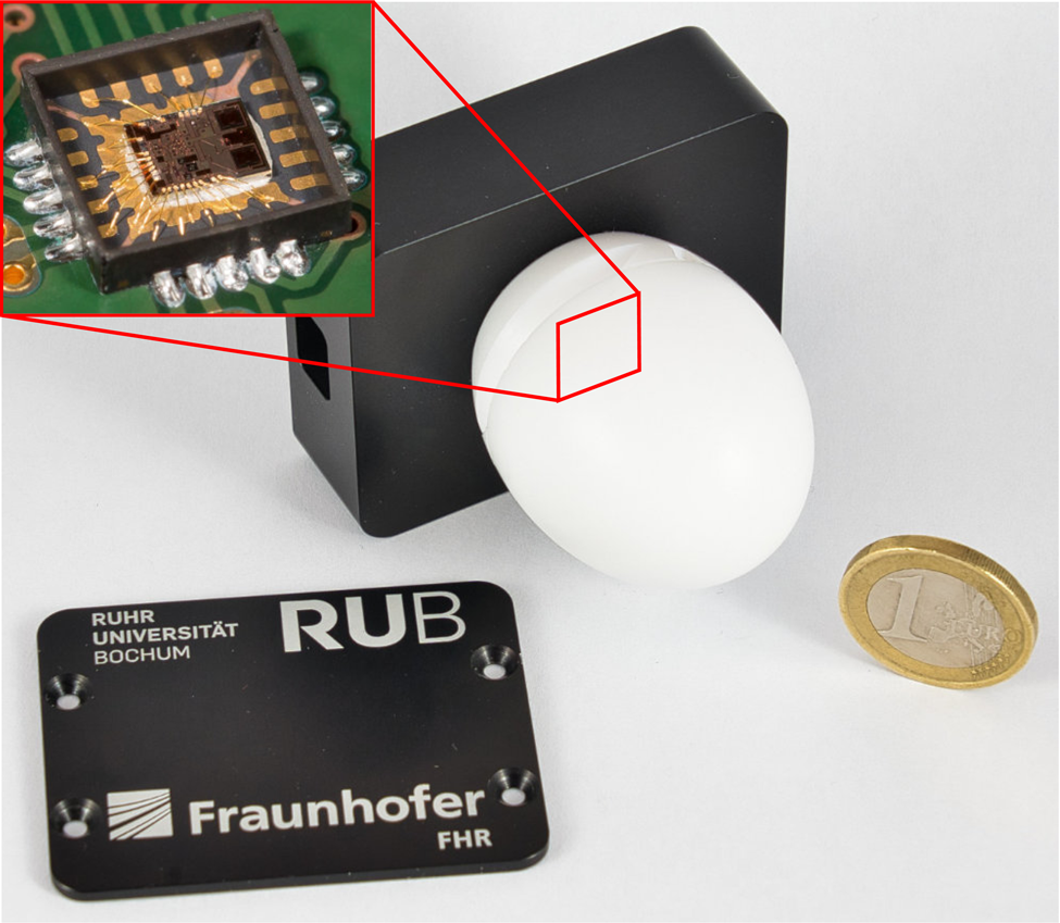
Fig. 1. Photograph of the compact radar sensor based on a self-developed 240 GHz SiGe transceiver MMIC [Reference Thomas, Shoykhetbrod and Pohl11].
The MMIC is fabricated in Infineons B11HFC SiGe BiCMOS technology and is carrying all high-frequency components on one die. With a maximum output frequency range of up to f out = 198 − 250 GHz, the output signal cannot be connected via bond-wires, as the losses by the parasitic series inductance would be too high. Therefore, the MMIC uses two on-chip antennas for TX and RX, respectively. To focus the wide radiation pattern of the on-chip antennas, a dielectric ellipsoidal lens antenna [Reference Pohl and Gerding12] is mounted on top of the MMIC. As the requirements of the antenna pattern depends on the specific measurement scenario, the use of an external lens is beneficial. Thus, antenna characteristics can be adjusted by scaling the lens dimensions according to the requirements of the desired application. As this demonstrator system is intended for demonstrating high precision distance measurements in industrial scenarios in confined environments, a high antenna gain combined with small sensor dimensions is desired. Therefore, in this scenario a default lens made from PTFE with a diameter of D lens = 36 mm is chosen, resulting in an antenna gain of approximately G lens ≈ 36 dBi, allowing a well-defined, small measurement spot combined with small sensor dimensions. The use of on-chip antennas allow a very compact realization of the whole sensor and a cost-effective assembly, as no signal beyond approximately 10 GHz occurs outside the MMIC. This enables the use of an open cavity Quad Flat No Leads (QFN) package for MMIC mounting on a standard FR-4 PCB material for the frontend-board. A detailed view of the mechanical assembly is depicted in Fig. 2.
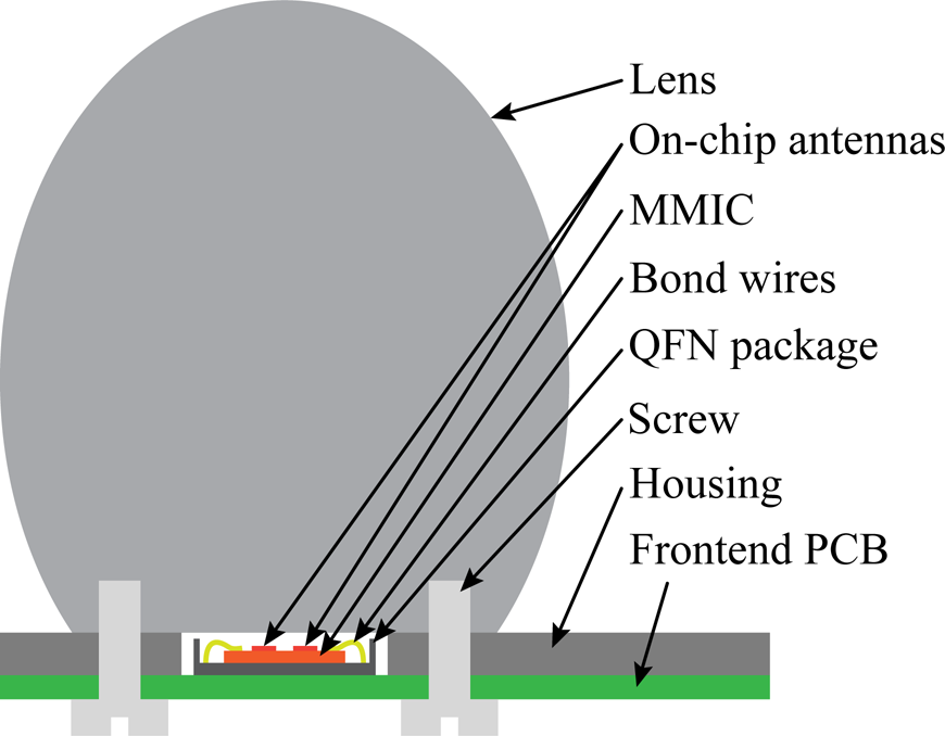
Fig. 2. Dielectric lens mounted on top of MMIC inside open cavity QFN package (cf. [Reference Thomas, Shoykhetbrod and Pohl11]).
The transceiver MMIC is mounted in the before mentioned QFN package on a frontend-board carrying the analog components like the phase locked loops (PLL) for FMCW ramp generation and an IF amplifier. The frontend-board is connected to a backend-board carrying the power supply circuitry, the PLL reference oscillator and the analog to digital converter connected to a micro-controller for data transmission and configuration via USB-interface as well as for configuring of the PLL modules. The overall block diagram of the sensor is depicted in Fig. 3.
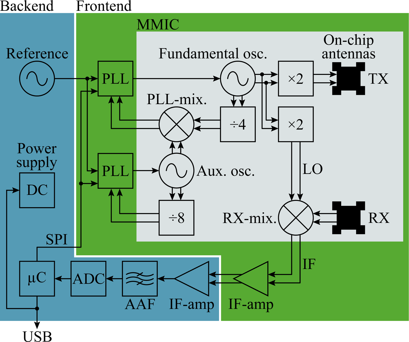
Fig. 3. Block diagram of the compact radar sensor including 240 GHz SiGe transceiver MMIC.
The modulation bandwidth of the sensor reaches B = 52 GHz within the frequency range from f ramp = 198 − 250 GHz. A detailed description of the whole sensor system including the used lens antenna is given in [Reference Thomas, Bredendiek and Pohl13].
Signal generation and false targets
The technology used for this MMIC, Infineons B11HFC SiGe BiCMOS technology, offers a maximum transit frequency of f T = 250 GHz, which represents a high value for commercially available, industrial grade high-speed SiGe technologies. Thus, the maximum operation frequency range of the sensor of f out = 198 − 250 GHz is very close to the maximum operation frequency of the technology, which limits the maximum output power, as no amplifiers with a sufficient gain are realizable at this frequency range. To generate an output power as high as possible, it is beneficiary to use a signal generation concept based on frequency multiplication. With a detailed look on Fig. 3, the transmit (TX) and local oscillator (LO) signal is generated by a fundamental oscillator, which has an operation frequency range from f fund = 99 − 125 GHz. This oscillator is implemented as a voltage controlled oscillator and stabilized by a dual-loop offset PLL as described in [Reference Pohl, Jaeschke and Aufinger14] to generate highly linear, wide-band FMCW ramps. As the frequency ramp is generated at half the operating frequency, subsequent frequency multipliers described in [Reference Thomas, Bredendiek, Jaeschke, Vogelsang and Pohl15] convert the signal to the wanted frequency range of f out = 198 − 250 GHz. An inherent drawback of the frequency multipliers is the limited isolation of the fundamental signal, which passes the multipliers parasitically in TX and LO direction, respectively. The parasitic TX signal is radiated, reflected by the target, received and then, in combination with the parasitic LO signal at the RX mixer, converted to IF-baseband, resulting in a false target in the range profile as depicted in Fig. 4.
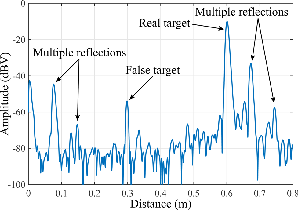
Fig. 4. Measured range spectrum of a single reflector in R = 0.6 m with false target at R false = 0.3 m.
In this measurement a single retro reflector was placed 0.6 m in front of the radar sensor without any other reflectors in the surrounding area. Close to the radar sensor multiple reflections from inside the dielectric lens antenna occur in the measurement, caused by TX signal ringing inside the lens. These multiple reflections are also observable behind the main target, as the RX signal is also ringing inside the lens. As these multiple reflections are at a fixed position for TX ringing and in a fixed distance to the main target for RX ringing, they can be removed by calibration and doesn't affect the measurement. Additionally, the false target at the exact half of the main target distance is clearly visible at a distance of 0.3 m. As this false target position is not fixed and moves with the main target and as the amplitude of the false target is not necessarily connected to the main target amplitude (depending on the main target properties), this false target cannot be calibrated. Therefore, it is not possible to distinguish the false target from an additional, weaker target which is actually present in the measurement path. This results in an unacceptable ambiguity for several industrial measurement applications.
Frequency filtering lens concept
To avoid the ambiguity mentioned above, the appearance of this false target has to be suppressed. A possible strategy to remove the false target is to avoid the parasitic feed-trough of the signal generation chain. As no additional power amplifiers or filter structures can be implemented on-chip due to the operation frequency close to the technologies f T, the doubler circuit is the main component for on-chip optimizations. Earlier versions of this transceiver used a Gilbert-cell-based frequency doubler, which caused a false target approximately 22 dB below the main target [Reference Jaeschke, Bredendiek and Pohl16]. Moving to the push-push-based doubler presented in [Reference Thomas, Bredendiek, Jaeschke, Vogelsang and Pohl15], the fundamental rejection could be approved, so the false target could be lowered to approximately 45 dB below the main target amplitude, as shown in Fig. 4. Due to the high dynamic range of the sensor, the false target is still visible approximately 23 dB above the sensors noise floor. To completely remove the false target, an additional external filtering technique is necessary. As radar sensors at lower frequencies allow an implementation of externals filter structures on high-frequency PCBs or an inherent filtering due to the cut-off frequency of waveguide components or antennas, this is not an option due to the use of on-chip antennas with no PCB or waveguide components involved. Therefore, an external free-space filter plate was introduced in [Reference Thomas, Bredendiek and Pohl13], based on a dielectric filter plate using interference effects as depicted in Fig. 5.
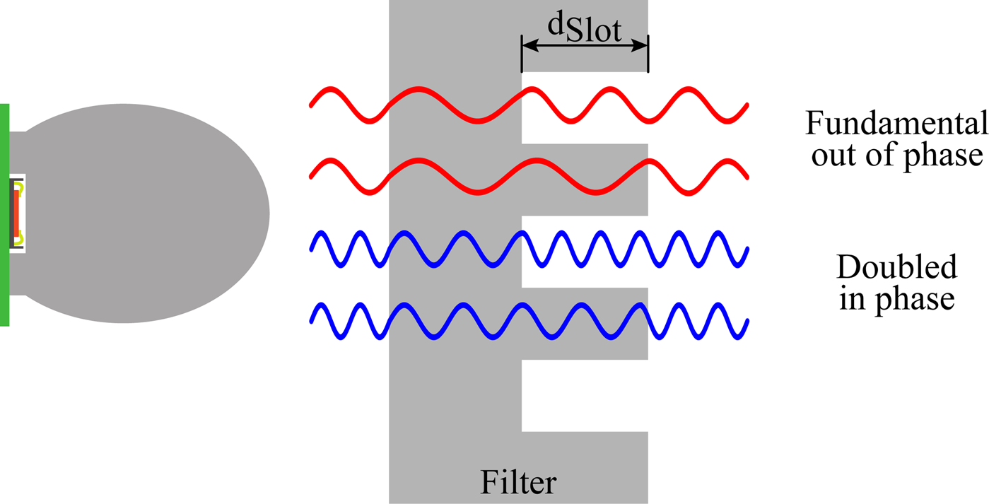
Fig. 5. Basic operation principle of interference filter, realized as an external filter plate (cf. [Reference Thomas, Shoykhetbrod and Pohl11, Reference Thomas, Bredendiek and Pohl13]).
The filter plate is made from a dielectric material, in this case PTFE, and is placed inside the measurement path between radar sensor and target. It is structured by several slots and bars, causing a different material thickness in different areas of the filter plate. To filter the parasitic feed-through signal, the phase difference between the signal parts transmitted through the thinned area (slot) and the full material thickness (bar) has to be 180°, causing a destructive interference, while the phase difference of the desired signal at the doubled frequency is 360°, causing a constructive interference. Thus, the fundamental feed-through signal is canceled out in the far field, while the desired signal is not affected by the filter at all. As the phase shift between the part of the signal propagated through a slot and the part of signal propagated through the full filter thickness is given by
the depth of the milled slots in case of PTFE as filter material has to be

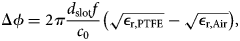
to achieve a destructive interference of the fundamental signal and a constructive interference of the desired signal (cf. [Reference Thomas, Bredendiek and Pohl13]). In Fig. 6 the successful filtering of the false target is demonstrated.
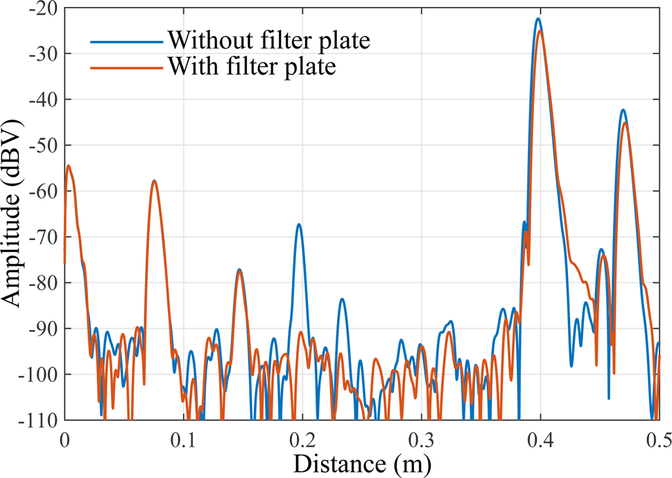
Fig. 6. Measured range spectrum from Fig. 4 compared to the measurement with filter plate from Fig. 5 (cf. [Reference Thomas, Bredendiek and Pohl13]).
To avoid the necessity of an external filter, in [Reference Thomas, Shoykhetbrod and Pohl11] this type of slotted interference filter structure was integrated in the dielectric lens used by this sensor. As the electric field, fed into the focus point of the lens by the on-chip antennas, propagates as spherical waves inside the lens, the filter structure is implemented alongside a spherical cutting plane through the lens body, as depicted in Fig. 7. Two types of filter structures were implemented, one with linear slots (Fig. 7(a)) and one with circular slots (Fig. 7(b)), respectively. For better illustration, the filter structures are shown as two separate parts, a base with the visible integrated filter structure at the bottom and a top part above with spherical cutting plane. Both parts are connected together to form the final lens geometry, ideally forming one solid component. The linear and circular types are based on the same operation principle described above, the only difference is the way the slots are aligned on the cutting plane.
Fig. 7. Two filter structures were integrated into the lens antenna, based on linear (a) and circular (b) slots (cf. [Reference Thomas, Shoykhetbrod and Pohl11]).
In Fig. 8 the simulated electric field inside the lens is shown. The lenses are fed by a linear polarized source, as the on-chip antennas on the transceiver MMIC are linear polarized as well. The E-field is polarized perpendicular to the slots, in-plane with the cutting plane in Fig. 8 As the cutting plane through the lens is chosen perpendicular to the filter slots, this depiction is valid for both filter structures, linear and circular, respectively.
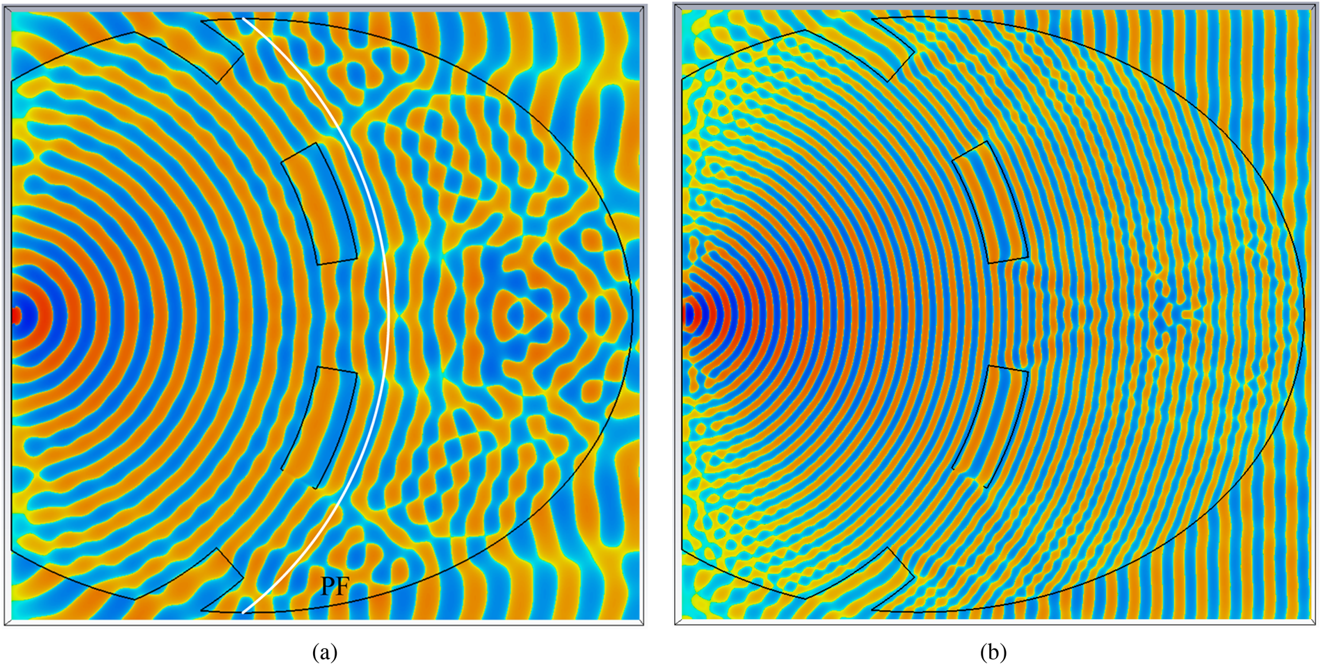
Fig. 8. Simulated electric field inside the lens at 110 GHz (a) and 220 GHz (b) [Reference Thomas17].
Figure 8(a) shows the electric field at a fundamental frequency of 110 GHz, the white line behind the filter structure represents a spherical phase front started from the feeding point of the lens. In front of the filter structure, the spherical character of the propagating wave inside the lens can be seen, hitting the filter structure homogeneously. Inside the channels of the filter structure, the lengthened wavelength causes the mentioned phase shift, clearly recognizable behind the filter structure. Along the white line, the phase of the electric field behind the channels is shifted 180° compared to the electric field propagated between the channels. This results in a destructive interference in the far field and therefore in a cancellation of the unwanted fundamental signal in main lobe direction. In contrast to this, Fig. 8(b) shows the electric field of the desired signal at a frequency of 220 GHz. Inside the filter structure channels, once again the lengthened wavelength can be seen, but in this case leading to a phase shift of 360° between the different parts of the wave behind the filter structure. Therefore, the spherical wave inside the lens is almost not affected by the filter structure at all, allowing the desired frequency to be radiated.
Both filter types are designed to be operated with a linear polarized feeding antenna, as the MMICs on-chip antennas are also linear polarized. Simulations have shown, that the circular slotted filter type is independent of the direction of polarization of the feeding antenna, as expected. The linear type is only independent of the direction of polarization, as long as the distance between the slots and the width of the slots itself is large compared to the wavelength. In this case, the distance between the slots and the width of the slots itself of the linear filter type is approximately 7~mm, which is larger than the wavelength. Thus, the linear type presented in this paper is independent of the direction of polarization of the feeding antenna, as well.
Fabrication of prototypes
Compared to the original solid lens without filtering structures, the overall size of the filtering lens is identical, as the filtering structures are only implemented inside the lens. In contrast to the solid lens, the fabrication of the filtering lens is much more complex. As the solid lens can be lathed or milled from a solid PTFE rod, the inner channels of the filter structure cannot be milled directly from one piece. Therefore, several approaches for manufacturing the antennas were compared.
Conventional milling
One option for a conventional fabrication by milling is, to separate the lens in two shaped by a spherical cutting plane alongside the filter structure as depicted in Fig. 7. Both components were fabricated separately and connected afterwards by dowel pins (cf. Fig. 7(b)). As the geometry of both parts is complex, this type of manufacturing is expensive but allows the use of PTFE as material, which is popular for dielectric lenses in this frequency range. Beside a reference antenna without filter structures, both filter types, with circular and linear slots, were fabricated, respectively. Figure 9 shows a photograph of the manufactured prototype with circular slots. Both parts are connected by dowel pins for alignment, forming the final filtering lens antenna.
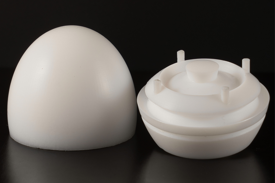
Fig. 9. Manufactured prototype made from PTFE with circular slots, both parts are connected by the dowel pins, forming the final filtering lens antenna [Reference Thomas17].
As second option, an additive manufacturing of the filtering lens is possible.
Additive manufacturing
Additive manufacturing or 3D-printing is a widely used term for a fabrication process in which an object is created layer by layer. In contrast to the conventionally used machining-based processes, material is selectively added instead of being removed. This feature enables the production of very complex shapes, beneficial for the present work. Two state-of-the-art additive manufacturing techniques, SLS and SLA were used to verify their suitability for the antenna fabrication presented in this work.
Stereolithography
In the SLA process, a UV light-sensitive liquid resin is used as the base material. The selective photopolymerization process is conducted by an UV-laser and a mirror-scanner. The laser sweeps over the surfaces along the path defined by the special software, the so-called slicer. As soon as the laser hits the liquid resin between the optical window and the build platform, it immediately solidifies. As soon as the entire layer is fully polymerized, it is pulled out of the liquid resin by a build platform. After the printing process is completed, the part is placed in a UV chamber to finalize the curing process. It should be noted that tensions are generated during the polymerization process, especially at overhangs steeper than 45 degrees. Support structures are therefore required to prevent deformation and cracking, and these must be removed in a post-processing step.
With this process, also complex structures can be printed easily. Also internal or concealed structures can be printed as long as hollow cavities have openings to allow unprocessed resin to be rinsed. Therefore, the linear type filtering antenna can be printed in one piece, while the circular type with closed channels needs to be printed in two parts, similar to the conventional milled antenna. Both SLA printed prototypes are shown in Fig. 10. Additionally a solid antenna as reference was printed as well.

Fig. 10. SLA printed filtering lens antennas of linear (a) and circular (b) type [Reference Thomas17].
Selective laser sintering
In contrast to SLA, in the powder bed process SLS, polymer particles are distributed by using a blade- or roller-coater. The infrared heat source heats the powder to just below the melting point. The carbon dioxide laser fuses the particles by scanning the surface of the distributed powder. The process step is completed by lowering the platform by one layer and the process cycle repeats until the entire part is finished. The completed part has to be removed and cleansed of unprocessed powder residue. The main advantage of this technology is based on the fact that the manufactured part is embedded in the unprocessed powder and does not require any support structures for overhanging elements [Reference Tomassoni, Peverini, Venanzoni, Addamo, Paonessa and Virone18]. Similar to the SLA printing process, concealed cavities need to be open to remove the unprocessed material, allowing the manufacturing of the linear filter type lens as one part, while the circular filter type lens needs to be printed in two parts and connected afterwards (Fig. 11).

Fig. 11. SLS printed filtering lens antennas of linear (a) and circular (b) type [Reference Thomas17].
Material characterization
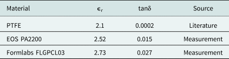
In order to perform a reliable antenna simulation, the electromagnetic properties of the used materials require extraction. As PTFE is a commonly used material for high-frequency dielectric lenses, the material parameters are well characterized and taken from literature (see Table 1). In contrast, the materials used for SLA and SLS printing are not commonly used for high-frequency applications, so their material parameters need to be determined. For determining the relative permittivity εr and loss tangent tanδ of the printing materials, a proprietary, commercially available, Material Characterization Kit (MCK) from Swissto12 is used. The metrological analysis is based on the quasi-guided free space wave method. The measurement assembly consists of two specially shaped waveguides and a flat-walled DUT. The corrugation on the inner walls of the waveguides creates a plane wave so that the entire surface of the sample is exited with the same phase. The sample itself should cover the entire aperture of the waveguide to avoid any inaccuracies. The dielectric constant and dielectric loss are extracted by a measurement software provided by Swissto12 as part of the MCK, processing the measured scattering parameters with a curve fitting algorithm. The DUT thickness can be determined to the accuracy of a micron with the built-in caliper gauge of the MCK fixture. Standard materials have been used for SLA (Formlabs FLGPCL03) and SLS (PA2200) manufacturing process. For each type of process, two square samples of size 40x40x4 mm were prepared to obtain the required dielectric parameters. All the material parameter measurements were performed in the V-band, since there was no suitable fixture available for the Y-band. Therefore, we had to rely on the measured material parameters at V-band for the simulations of the lenses in the Y-band. In section “Material losses” the material losses extracted from radar measurements recorded with the reference antennas made from different materials are compared to the simulated material losses to verify the measured material parameters at V-band. An overview of the material parameters used for the antenna simulations are shown in Table 1.
Table 1. Material parameters used for antenna dimensioning and simulation
Simulations
For simulating the reference and frequency filtering lens antennas, CST Microwave Studio was used. The lenses were fed by an waveguide port, dimensioned to excite a similar wave pattern compared to the on-chip antennas on the MMIC. This is done to minimize the simulation time, as a simultaneous simulation of the on-chip antenna with micrometer dimensions and the lens with millimeter dimensions leads to a huge computational effort, resulting in a long simulation time.
Filtering performance
For simulating the filtering effect in main lobe direction, the antenna gain G filter, 110 was simulated at a fundamental frequency of 110 GHz and compared to the simulated antenna gain G ref, 110 of a solid reference lens with the same dimensions without filtering structure:

The difference in gain between reference and filtering lens in main lobe direction represents the attenuation of the fundamental signal in main lobe direction caused by the filter structure and is printed in Table 2.
Table 2. Attenuation of frequency filtering lens in comparison with reference lens, based on simulated antenna gain
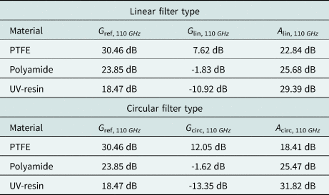
The simulated attenuation of the fundamental signal caused by the filter structure varies from A min = 18.41 dB for the circular type made from PTFE and A max = 31.82 dB for the circular type made from SLA resin. Despite the difference in attenuation over the different variants, the functionality of the filter structure could be shown. The variation of the attenuation across the different types of material and filter structure type needs to be further investigated. As the values of the attenuation remain nearly the same if they are calculated with the directivity instead of the antenna gain, an influence of the material losses could be excluded at this point. For the different materials, the outer radius of the lens was kept constant to maintain the effective antenna aperture. Therefore, the lens gets shorter with increasing εr. This change in geometry does also affect the filtering effect of the structure inside the antenna. As the center frequency of the filter effect is determined by the depth of the slots according to equation (2), the parameters of slot width and spacing are free to be chosen. By optimizing the width and spacing between the slots, the filter effect might be optimized, minimizing the variation of the attenuation across different material types.
In contrast to the attenuation calculated by the difference in antenna gain at fundamental frequency for reference and filtering lens, a more practical application-driven approach is to investigate the effective attenuation calculated by the difference in antenna gain for fundamental frequency and desired frequency of the same antenna:

With this type of effective attenuation the filter performance to remove false targets using this antenna is described better, as several additional effects are taken into account. On the one hand, the use of the same lens antenna at the doubled desired signal (220~GHz) compared to the fundamental signal (110 GHz) increases the antenna gain due to the larger antenna aperture relative to the wavelength, which would increase the filtering effect between desired and fundamental signal. On the other hand, toward higher frequencies the dielectric losses caused by the loss tangent tanδ increase, as well. This effect reduces the filtering effect between desired and fundamental signal, as the desired signal suffers from higher dielectric losses as the fundamental signal. Additionally, this definition of the effective attenuation also considers the losses for the desired signal induced by the filter structure. The calculated effective attenuation for the different antennas is given in Table 3.
Table 3. Difference in antenna gain of frequency filtering lens at fundamental frequency (110~GHz) im comparison with antenna gain at desired frequency (220~GHz), representing the effective attenuation of the fundamental signal compared to desired signal
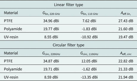
For PTFE as lens material, the effective attenuation is larger compared to the attenuation caused by the filter structure itself from Table 2, meaning the PTFE filtering lens antenna offers an increased performance for filtering the fundamental signal. As PTFE with a loss tangent of tanδPTFE = 0.0002 is a low loss material, the before mentioned effect of increasing the effective attenuation by increasing the antenna gain toward higher frequencies dominates. The effect of lowering the effective attenuation by an increased dielectric loss at higher frequencies is minor in this case. The maximum effective attenuation is achieved with the linear filter type lens antenna made from PTFE with A eff, lin, PTFE = 27.43 dB and an antenna gain for the desired signal of G lin, PTFE, 220GHz = 34.96 dBi. According to Table 1, the loss tangent, and therefore the dielectric losses, is much stronger for polyamide (tanδPA = 0.015) and UV-resin (tanδResin = 0.027). This leads to a domination of the effect of lowering the effective attenuation by increased losses for the desired signal. Compared to the values of the attenuation from Table 2, the filter effect is reduced by several dB, down to approximately A eff, PA/UV, lin/circ ≈ 19.47.. 21.94 dB according to Table 3.
To determine the losses of the filter structure for the desired frequency, the antenna gain of the reference lens without filter structures at a desired frequency of 220 GHz was compared to the antenna gain of the filtering lens at the same frequency:

The simulated values for the attenuation of the desired signal by the filtering structures are shown in Table 4.
Table 4. Attenuation of the desired signal by the frequency filtering structure inside the lens antenna
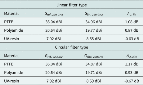
The influence of the filter structure on the desired signal is very low with a maximum attenuation of A D, circ, PTFE = 1.17 dB. With increasing material losses the attenuation decreases. This results in the interesting effect, that for UV-resin, the material with the highest losses used in this work, the attenuation gets negative, thus, the antenna gain for the desired frequency could be improved by the filtering structure. This effect is explained by the material losses in the area of the filter structure. As the filter structure is realized by adding air-filled slots in the antenna, the material losses in this area are much lower compared to the lossy surrounding UV-resin material. Therefore, if the material losses are high enough, the reduced overall dielectric losses dominate the disturbance of the wave propagation due to the filter structure itself, leading to an improved antenna gain. Nevertheless, as the attenuation of the desired signal caused by the filter structure is small with values from A D = −0.67 to 1.17 dB, the influence of the filter structure can be neglected.
Summarized, considering the effective attenuation based on the difference in antenna gain at fundamental and desired frequency, the use of a low loss material like PTFE is beneficial compared to lossy material like polyamide or UV-resin.
Side lobes
Another important aspect of the antenna performance is the side lobe behavior. As the energy at the fundamental frequency is not completely reflected by the filter structure, it gets radiated into the side lobes of the lens antenna. A three-dimensional far field simulation at a fundamental frequency of 110 GHz of both filter types made from PTFE is shown in Fig. 12.

Fig. 12. Simulated far field at fundamental frequency (110 GHz) for linear (a) and circular (b) type of filtering lens antenna made from PTFE. The color scaling of both plots is identical.
In the upper part (Fig. 12(a)) the far field of the linear slotted filter structure is shown. The filter slots are aligned horizontally, resulting in a vertically split antenna pattern, as the energy of the fundamental signal is mainly distributed in two separate side lobes. The maximum gain of the side lobes is simulated to be G SL, lin, PTFE = 25.4 dBi. Compared to the antenna gain in main lobe direction at the desired frequency of G lin, PTFE, 220 GHz = 34.96 dBi, the relative side lobe level or effective attenuation of the desired signal in main lobe direction to the fundamental signal in side lobe direction is A eff, SL, lin = 9.56 dB, still representing a significant filter effect, but not sufficient to completely remove the false targets in side lobe direction. Thus, the linear type of filter structure might be limited to well-defined and controlled measurement environments, where other targets or reflectors in side lobe direction can be excluded. The side lobe direction is approximately Θ SL, lin = ±8°, which can be influenced by the slot width and distance of the filter structure and might be optimized depending on the specific use case.
In the lower part (Fig. 12(b)) the far field of the circular slotted filter structure is shown. In contrast to the far field of the linear filter type, the circular filter type distributes the main part of the radiated fundamental signal energy in a rotational symmetric way around the main lobe direction, thus, leading to a significantly lower side lobe amplitude. The side lobe direction is once again at approximately Θ SL, circ = ±8°, and can be controlled by the slot width and distance, too. As the color scaling of both plots are identical, the maximum side lobe amplitude for the circular type is G SL, circ, PTFE = 18.14 dBi. Compared to the antenna gain in main lobe direction at the desired frequency of G circ, PTFE, 220 GHz = 34.87 dBi, the relative side lobe level or effective attenuation of the desired signal in main lobe direction to the fundamental signal in side lobe direction is A eff, SL, circ = 16.73 dB, which represents an improvement of 7.17 dB compared to the linear type. Therefore, the achieved side lobe level should be sufficient to suppress false targets in side lobe direction almost completely.
Summarized, the circular filter type is the more versatile variant, even for measurement environments with several parasitic reflectors in side lobe direction, while the linear filter type offers slightly more fundamental suppression in main lobe direction (cf. Table 3).
Measurements
To verify the functionality of the proposed frequency filtering lens, the manufactured lens prototypes were mounted on the FMCW radar sensor described in section “Used radar sensor”. An FMCW bandwidth of B = 52 GHz (from 198 to 250 GHz) was used to show the wide-band operation capabilities of this antenna concept. The sweep bandwidth was configured to be T Ramp = 15 ms. In the following measurements, the material losses, filter performance, and side lobe behavior are analyzed in detail.
Material losses
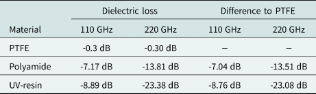
As mentioned in section “Material characterization”, the measurement equipment for characterizing the material parameters of Polyamide and Formlabs resin was only available at V-band. Therefore, we had to adopt the measured material parameters to be valid at Y-band, as well. Additionally, no antenna measurement assembly was available at Y-band, to measure the absolute antenna gain diagram, to compare simulations and measurements. Thus, we determined the material losses inside the lens material to verify the measured material parameters. The simulated dielectric losses inside the reference lenses made from different materials without filtering structures is given in Table 5.
Table 5. Simulated dielectric loss in the lens material for the reference lenses without filtering structure
Additionally, radar measurements with a single target at a distance of 0.6 m were recorded with reference lens antennas made from different materials, which are depicted in Fig. 13(a). In these measurements, the difference of the target amplitudes among different lens materials is mainly determined by the dielectric loss inside the lens material. As the signal passes the antenna two times in radar operation (TX and RX), the influence of the material loss is doubled in this case. The measured target amplitudes for the different reference lenses is shown in Table 6.

Fig. 13. Range plots measured with the frequency filtering lens antennas made from different materials, compared to reference antenna of the same material.
Table 6. Measured target amplitude for the reference lenses without filtering structure
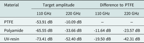
To finally compare the simulated and measured values, the difference in material loss between each additive manufactured lens and the lens made from PTFE as well known, low-loss, material is observed. So the difference in simulated material loss between Polyamide and PTFE or Formabs resin and PTFE should be the same as half the difference in measured target amplitude between Polyamide and PTFE or Formabs resin and PTFE. Here, half of the difference in measured target amplitude is used, as in the measurement the signal passes the lens two times, while in the simulation the one-way loss is determined. The measured and simulated difference in material loss compared to the PTFE reference lens is shown in Table 7.
Table 7. Measured and simulated difference in material loss compared to PTFE reference lens
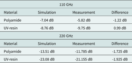
With a maximum deviation of 1.925 dB the simulation and measurement of the difference in material loss between Polyamide or Formlabs resin and PTFE fits very well. Thus, the material parameters measured at V-band are also valid in the Y-band with sufficient accuracy.
Filtering performance
For analyzing the filtering effect, a single retro reflector was mounted in a distance of D target = 0.6 m in front of the sensor, while the surrounding area of the measurement environment was kept clear of additional parasitic reflectors. Therefore, the ideal range spectrum should only contain a single target at 0.6 m. For every material, a measurement was recorded using the reference antenna without any filtering structure, the linear type frequency filtering lens, and the circular type frequency filtering lens. The measured range spectra are shown in Fig. 13.
The top plot (Fig. 13(a)) shows the comparison of all three reference antennas made from different materials. First of all, all three measurements show a clear main target at D target = 0.6 m and the corresponding false target at D false = 0.3 m. The amplitude of these targets elucidates the increasing material loss from PTFE over polyamide to UV-resin. As the dielectric losses are higher at the desired frequency than at fundamental frequency, the main-to-false-target ratio (MFR) reduces with increasing material losses. Thus, for PTFE as lens material the false target is MFR PTFE, ref = 43.82 dB below the main target amplitude, while for polyamide and UV-resin the false target amplitude is MFR PA, ref = 31.88 dB and MFR UV‒resin, ref = 21.01 dB below the main target amplitude, respectively. Additionally, the multiple reflections described in section “Signal generation and false targets” (cf. Fig. 4) are much stronger for the PTFE antenna compared to the additive manufactured antennas. This is also caused by the material losses. As these multiple reflections are caused by ringing of the TX and RX signal inside the lens, it passes the lens multiple times, each time getting attenuated by the dielectric losses. Therefore, the multiple reflections inside the antenna are much more affected by the dielectric losses than the measurement signal, which passes the antenna solely two times (TX and RX). In Fig. 13(b)–(d) the measured range spectrum recorded with the filtering lens antennas is shown. Compared to the reference measurement, the false target could be removed completely with the help of the frequency filtering lens. As the false target amplitude is approximately 23 dB above the noise floor for PTFE, it can be proofed, that the measured attenuation of the false target has to be at least A eff, PTFE = 23 dB for both filter types, which fits well with the simulated value of A eff, circ, PTFE = 22.82 dB for the circular type PTFE antenna. As the signal to noise ratio of the false targets in the other measurements is much lower than the simulated effective attenuation, it only can be shown, that the measured suppression is sufficient to completely remove the false target, without numbering the exact suppression ratio. In case of the PTFE lenses, the multiple reflections of the antennas with filtering structures appear worse compared to the reference antenna. This is due to the additional scattering and reflections of the wave at the filtering structure, increasing the ringing effect. The same ringing occurs at the other antennas made from another material, but gets attenuated by the higher dielectric losses as mentioned before. As these reflections are caused by the geometrical dimensions of the lens, they are fixed in position and can be removed by calibration.
Side lobes
Additionally, the effects of the side lobe distribution described in the subsection “Side lobes” within section “Simulations” were analyzed. For each antenna, the sensor was aligned according to the side lobe direction simulated for each antenna (approximately 8°) toward the same retro reflector used in the measurements above. The recorded range spectra are shown in Fig. 14.

Fig. 14. Range plots measured with linear and circular type of frequency filtering lens in side lobe direction.
For PTFE (Fig. 14(a)) and polyamide (Fig. 14(b)) the false target appears in the measurements of the linear type filtering lens, while in the measurements recorded with the circular type the false target cannot be seen. This corresponds to the simulations, as the side lobe level of the linear filter type at fundamental frequency is only A eff, SL, lin = 9.56~dB below the main lobe amplitude at the desired frequency, which is not sufficient to completely remove the false target. It has to be mentioned, that this is only the case, if the side-lobe directly hits another reflector, as the side lobe of the linear type is only a sharp pencil beam (cf. Fig. 12(a)). In contrast, the side lobe level of the circular type is low enough to completely remove the false target from the measurement. As the side lobe of the circular type is distributed around the main lobe, as depicted in Fig. 12(b), the possibility of hitting another reflector is higher, but due to the lower amplitude does not affect the measurement. For the measurements recorded with the UV-resin lenses in Fig. 14(c) this effect is not visible, as the dielectric losses are too high to detect the side lobe reflection.
Conclusion
Based on the original conference paper [Reference Thomas, Shoykhetbrod and Pohl11], a novel frequency filtering dielectric lens concept was demonstrated. In many modern radar sensors based on SiGe MMICs, the signal generation is realized with a fundamental oscillator at a lower frequency followed by frequency doubler circuits. The limited fundamental isolation of the frequency doubler causes a fundamental feed-through signal, which may cause false targets at half distance in the range spectrum. These false targets affect the reliability of the measurements as those false targets cannot be distinguished from real targets at half distance, limiting the usability of the sensors for measurement scenarios where an unambiguous measurement is inevitable, especially in the field of industrial measurement applications. The proposed frequency filtering lens antenna is based on an interference filter structure that is integrated into the lens antenna, canceling the fundamental feed-through signal by destructive interference while the desired doubled frequency is not affected. Two types of filtering structures were developed, based on linear and circular slots inside the lens. As the complex geometry is beneficially for additive manufacturing, multiple prototypes were fabricated, using SLA and SLS printed lenses as well as conventional milled lenses made from PTFE. All filter types and material combinations were compared in terms of filtering performance and side lobe behavior with simulations and measurements. Summarized, all lens antennas were able to successfully remove the false target from the measurement, thus, fixing the ambiguousness, previously avoiding the usability of the sensor for several industrial applications.
Conflict of interest
None.
Biography
 Sven Thomas was born in Bochum, Germany, in 1987. He received the M.Sc. and Dr.-Ing. degrees in electrical engineering from Ruhr University Bochum, Germany, in 2013 and 2021, respectively. Since 2013, he has been a Research Assistant with the Department of Integrated Circuit and Sensor Systems, Fraunhofer Institute for High Frequency Physics and Radar Techniques, Wachtberg, Germany. His current research interests include the design of integrated SiGe circuits and the development of system and antenna concepts for industrial radar-based measurement systems with operating frequencies up to 300 GHz. He was a recipient of the Argus Award of Cassidian in 2012 and was a co-recipient of the EuMIC Best Paper Award from the European Microwave Week in 2012 and the 2015 Best Demo Award of the IEEE Radio Wireless Week.
 Alex Shoykhetbrod was born in 1983 in Odessa, Ukraine. Alex received his Dipl.-Ing. Degree in Communication Engineering from the University of Applied Sciences Koblenz, Germany in 2009. In 2012, Alex received his Masters of System Engineering from the University of Applied Sciences Koblenz, Germany. In 2009, Alex joined Fraunhofer Institute for High Frequency Physics and Radar Techniques's Team in Wachtberg, Germany where his research interests have included development of FMCW Radar Systems, PCB Design and Application of Additive Technology in mm-Wave field.
 Nils Pohl received the Dipl.-Ing. and Dr.Ing. degrees in electrical engineering from Ruhr University Bochum, Bochum, Germany, in 2005 and 2010, respectively. From 2006 to 2011, he was a Research Assistant with Ruhr University Bochum, where he was involved in integrated circuits for millimeter-wave (mm-wave) radar applications. In 2011, he became an Assistant Professor with Ruhr University Bochum. In 2013, he became the Head of the Department of mm-wave Radar and High Frequency Sensors with the Fraunhofer FHR, Wachtberg, Germany. In 2016, he became a Full Professor of Integrated Systems with Ruhr University Bochum. In parallel, he is the Head of the Research Group for Integrated Radar Sensors at Fraunhofer FHR. He has authored or coauthored more than 200 scientific papers and has issued several patents. His current research interests include ultra-wideband mm-wave radar, design, and optimization of mm-wave integrated SiGe circuits and system concepts with frequencies up to 500 GHz and above, as well as frequency synthesis and antennas. Prof. Pohl is a member of VDE, ITG, EUMA, and URSI. He was a co-recipient of the 2009 EEEfCom Innovation Award. He was a recipient of the Karl-Arnold Award of the North Rhine-Westphalian Academy of Sciences, Humanities and the Arts in 2013 and the IEEE MTT Outstanding Young Engineer Award in 2018. Additionally, he was co-recipient of the Best Paper Award at EUMIC 2012, the Best Demo Award at RWW 2015, and the Best Student Paper Awards at RadarConf 2020, RWW 2021, and EUMIC 2021.


 Open access