


Introduction
Planar antennas are receiving a lot of attention in research and in the wireless industry due to their advantages such as small size, low profile, simple configuration, economical cost, and ease of integration with other high-frequency devices [Reference Agrawall, Kumar and Ray1, Reference Liang, Chiau, Chen and Parini2]. These antennas are best suited for short-range communications, peer-to-peer ultrafast communications, and other high data rate modern wireless applications [Reference Chen, Ammann, Qing, Wu, See and Cai3, Reference Chen4]. Recently, multiple-input-multiple-output (MIMO) antenna structures have drawn substantial attention because of their ability to adapt the exponentially increasing traffic environment. The concept of MIMO is very helpful in decreasing multipath fading effects, thus attaining higher data rate, range, and reliability without increasing the spectrum range or transmit power [Reference Rajagopalan, Gupta, Konanur, Hughes and Lazzi5]. To achieve a high-performing MIMO system, several antenna elements are usually integrated together with low mutual coupling between the antenna ports [Reference Kumar, Kumar, Vishwakarma and Srivastava6]. However, due to the limited available space in portable devices, the adjustment of several antenna elements inside the device is a difficult task. Because of multiple closely-operating bands and space restrictions, the radiating antenna unit cells are exposed to large inter-element coupling, which degrades the system performance [Reference Saxena, Kanaujia, Dwari, Kumar and Tiwari7]. In the last few years, a number of MIMO antennas have been reported by many investigators [Reference OuYang, Yang and Wang8–Reference Ramachandran, Pushpakaran, Pezholil and Kesavath12]. In [Reference OuYang, Yang and Wang8], an antenna structure with two radiating elements was proposed with a common ground plane. The antenna presented in [Reference Khan, Capobianco, Asif, Anagnostou, Shubair and Braaten9] was comprised of a complementary split ring resonator-loaded ground plane and two counter facing monopole radiators. A MIMO antenna structure with two upturned F-shaped radiators for dual operating bands was proposed in [Reference Deng, Li, Zhao and Guo10]. A MIMO antenna design consisting of four L-shaped unit cells integrated with an split ring resonator structure was reported in [Reference Sarkar and Srivastava11]. In [Reference Ramachandran, Pushpakaran, Pezholil and Kesavath12], a four-port MIMO antenna loaded with concentric square loops was presented.
Another configuration, which is in high demand for emerging wireless applications, is circularly-polarized (CP) MIMO devices [Reference Saxena, Kanaujia, Dwari, Kumar and Tiwari13]. CP antennas are broadly used for Bluetooth, RFID, WLAN, WiMAX, satellite, and radar applications. CP MIMO antennas have the benefit of large spectral efficiency since these antennas do not possess the difficulty of polarization mismatch between the transmitter and receiver. However, among the existing MIMO antenna designs, only a few have been proposed with circular polarization characteristics. A dual-port MIMO antenna with an inductor-loaded metal strip for CP radiation was presented in [Reference Qu, Piao and Qu14]. In [Reference Choukiker, Sharma and Behera15], a two-port MIMO antenna making use of the fractal Koch and Minkowski island curves and the defected ground for obtaining high isolation was proposed. A two-port MIMO antenna with cross-branch implanted in the ground surface for circular polarization was reported [Reference Yao, Wang, Chen, Yu and Liu16]. A MIMO antenna with two radiators located on the top and bottom sides of the substrate was presented in [Reference Malik, Patnaik and Kartikeyan17]. A triple-port MIMO antenna making use of the corner truncation technique for achieving CP band was proposed in [Reference Sharma, Sarkar, Saurav and Srivastava18], and four rectangular radiators with truncated corner and loaded with 90° apart rectangular slots in the center was proposed in [Reference Malviya, Panigrahi and Kartikeyan19]. A quad-port MIMO antenna with corner truncated patch for circular polarization was designed in [Reference Parbat, Tambe, Kadu and Labade20], and four symmetrical triangular monopole radiators were placed orthogonally in [Reference Kayabasi, Toktas, Yigit and Sabanci21]. In [Reference Akbari, Ghalyon, Farahani, Sebak and Denidni22], a multi-layered, aperture-coupled, cross-slot MIMO antenna with circular polarization was proposed. However, in most of the reported designs, the ground planes of the antenna elements were not connected with each other, thereby leading to shifting reference voltages [Reference Sharawi23]. Also, the complex elements in the radiator or ground surface increases the antenna dimension and design complexity, hence making the proposed antennas difficult to be integrated with monolithic microwave integrated circuits (MMICs) or other high-frequency circuits.
In this paper, a new design method of a planar CP MIMO antenna consisting of four closely-placed unit cells of antenna elements with connected ground is presented. The MIMO antenna must have a common ground plane so that all signal levels within the MIMO system can be interpreted correctly based on the same reference level. If separate and not-connected ground planes are present, the MIMO antennas may not work in practical applications since the assumption of having all ground surfaces with the same voltage level becomes invalid. Furthermore, the decoupling method using defected ground structure is only valid when the ground planes of radiating elements are not completely separated. The implemented antenna has compact size and provides very wide impedance bandwidth and axial ratio bandwidth. The proposed MIMO antenna shows high isolation between elements over a wide range of frequencies. It also exhibits good diversity performance making the proposed antenna suitable for ultra-wideband (UWB) MIMO systems in the presence of multipath fading. With attractive features of a simple structure and UWB operation, the proposed MIMO antenna can be used for wireless personal area networks. The obtained results agree well with the simulated outcomes.
Antenna structure
Design of a CP antenna element
The schematic of the proposed antenna is illustrated in Fig. 1. The proposed antenna consists of a microstrip feed line on the top side of the substrate and a ground plane on the bottom side of the substrate. A 50 Ω microstrip feed line is used for exciting the antenna structure, and a wide slot is introduced in the ground plane of the antenna. Further, in order to realize CP operation in the proposed structure, a circular stub protruded from the ground conductor strip is formed. The feed line of the antenna is positioned near the circular stub to broaden the axial ratio bandwidth of the unit cell. The FR-4 dielectric substrate with a relative permittivity of 4.4, thickness of 1.6 mm, and loss tangent of 0.02 is used for the design of the proposed antenna. The design parameters of the proposed unit cell are given in Table 1. A 3-D EM simulator (Ansys HFSS®) is used for designing the proposed structure.

Fig. 1. Geometry of the proposed antenna element: (a) top view and (b) side view.
Table 1. Dimensions of the proposed antenna

The antenna designing steps are illustrated in Fig. 2. First, the side length of the square conductor patch is calculated by the relation [Reference Balanis24]
 $$f_c = \displaystyle{c \over {2\sqrt {\varepsilon _r} }}\sqrt {{\left( {\displaystyle{m \over {L_1}}} \right)}^2 + {\left( {\displaystyle{n \over {L_1}}} \right)}^2}$$
where f c is the center frequency, c is the speed of light in free space, ε r is the relative permittivity of the substrate, L 1 is the length of the square conductor patch, and m and n are resonating modes. The width of the microstrip line feed is calculated as [Reference Blackwell25]
 $$W_f = \displaystyle{{7.48 \times h} \over {e^{\left( {Z_o(\sqrt {\varepsilon _r + 1.41} /87)} \right)}}}-1.25 \times t$$
where W f is width of the feed line, h is thickness of the dielectric substrate, Z o is the input impedance, and t is the trace thickness. Next, as shown in Fig. 2(a), a wide slot is formed inside the conventional square-shaped antenna (antenna 1), which is an ordinary wide slot antenna excited by the 50 Ω microstrip feed line located at the center of the wide slotted ground surface. The dimensions of the wide slot affect the current path, which changes the resonating frequency band of the antenna. In Fig. 2(b), a circular stub is protruded toward the center of the wide slot in the ground plane of the antenna (antenna 2). In antenna 3 shown in Fig. 2(c), the feed line is shifted toward the right edge of the antenna near the protruded circular stub. When the feed is at the center (antenna 2), the EM energy is distributed symmetrically throughout the wide slot. Alternatively, varying the feed line location significantly improves the impedance matching without using any additional matching element. The ground plane with the circular stub and the offset feed line position induces a wide CP band within the antenna resonating range. Furthermore, a part of the ground plane underneath the feed line is removed to reduce the coupling between the feed line and ground surface.
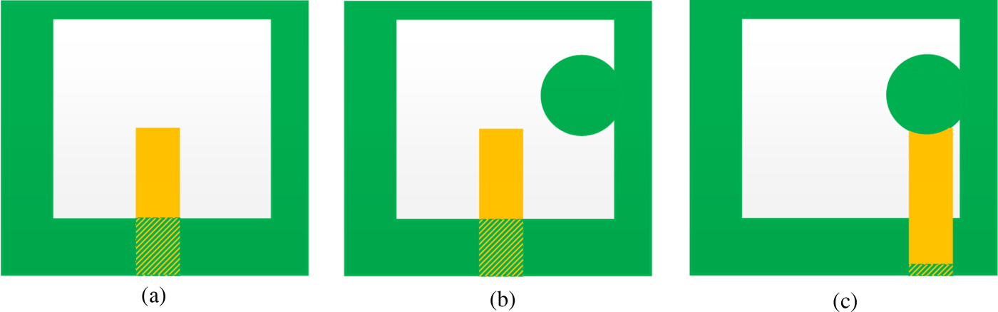
Fig. 2. Design steps of the unit cell antenna: (a) antenna 1, (b) antenna 2, and (c) antenna 3.
Figure 3(a) shows the comparison of the simulated reflection coefficients for the antenna design evolution steps as illustrated in Fig. 2. Antenna 1 is an ordinary square-shaped antenna with a wide slot in the ground plane and excited by a microstrip feed line. Antenna 1 shows a wide impedance bandwidth of 4.6 GHz (3.9–8.5 GHz) as can be seen in Fig. 3(a). Figure 3(b) shows the axial ratio comparison of antenna evolution steps. As can be seen, antenna 1 with a wide slot in the ground plane is linearly polarized. Antenna 2 with a circular stub protruded from the ground conductor strip improves the reflection coefficient characteristics in both upper and lower frequency ranges. This improvement in impedance bandwidth is due to the increased current path induced by the circular stub in the ground plane. Further, the circular stub introduces a 90° phase difference between E xoy and E yoz components, which is required for obtaining circular polarization, and, as a result, the axial ratio reduces to approximately 1 dB in the antenna radiating band range. To considerably improve the 3 dB axial ratio bandwidth, the microstrip feed line is offset-positioned near the right edge of the ground surface just beneath the circular stub. Moreover, to improve the impedance bandwidth and circular polarization characteristics, a part of the ground strip beneath the feed line is etched out, hence reducing the mutual coupling effect between the feed line and ground plane (antenna 3). This increases the axial ratio bandwidth to 3.7 GHz ranging from 4 to 7.7 GHz.

Fig. 3. Comparison of the antenna design steps: (a) reflection coefficient and (b) axial ratio.
To realize a very wide axial ratio bandwidth from the proposed antenna, the radius and location of the protruded circular stub are optimized by varying one of the parameters while keeping the other parameters fixed. The parametric study of the size of the circular stub and its position along the y-axis is illustrated in Figs 4(a) and 4(b), respectively. It can be observed from Fig. 4 that the most favorable results are achieved with D s = 7.2 mm and h 1 = 11 mm. The surface current distribution and far-field radiation pattern of proposed antenna 3 at 5.75 GHz are shown in Figs 5 and 6(a), respectively. Stronger fields are concentrated close to the protruded circular stub in a clockwise rotation. The direction of the current vectors is clockwise in both antennas 2 and 3, hence validating the left-hand circularly-polarized (LHCP) operation of the antenna. The gain of the antenna unit cell is shown in Fig. 6(b). A peak gain of 3.6 dBi and average gain around 3 dBi are obtained in the operating band. A comparison of the proposed antenna with other reported CP antennas is given in Table 2. Unlike other reported CP antenna designs [Reference Ding, Gao, Qu and Yin26–Reference Yang, Kishk and Lee34], the proposed antenna structure is extremely compact, low profile, and can be easily designed since it does not implicate any truncation of the patch or loading of active devices. The antenna exhibits an ultra-wide impedance and axial ratio bandwidth of 112 and 63%, respectively.

Fig. 4. Axial ratio variations with different values of (a) D s and (b) h 1.

Fig. 5. Surface current distributions at 5.75 GHz: (a) ωt = 0°, (b) ωt = 90°, (c) ωt = 180°, and (d) ωt = 270°.

Fig. 6. Proposed antenna element: (a) radiation pattern at 5.75 GHz and (b) gain variation.
Table 2. Comparison of the proposed antenna element with other reported antennas
Design of a two-port CP MIMO antenna
In designing a compact two-port MIMO antenna, the proposed antenna element with dimensions of 20 × 20 mm2 is to be organized in a 1 × 2 pattern as shown in Fig. 7. The overall dimensions of the proposed two-port MIMO antenna are 45 × 20 × 1.6 mm3. It is important to note that, as the antenna elements are placed close to each other in the MIMO antenna, the value of axial ratio is deteriorated as compared with that of the unit cell antenna, and becomes greater than 3 dB at many points in the band of interest. This deterioration in the axial ratio is due to the strong interference from the adjacent antenna elements. For overcoming this interference, a rectangular-shaped strip is introduced on the ground surface, which reduces the level of interference between the two adjacent antenna elements by reflecting EM radiations from closely-packed antenna elements, thereby restoring the axial ratio bandwidth. In multi-antenna systems, the isolation between antenna elements can be increased through decoupling elements or by introducing enough space between the radiators. But, a large spacing between antenna radiating elements will increase the overall size of the antenna. In the proposed design, a rectangular-shaped strip is used for reducing interference between the adjacent antenna elements, minimizing space between the antenna elements. The spacing and position of the strips are optimized in such a manner that a compact geometry (with minimum inter-element coupling and wide 3 dB axial ratio bandwidth) is achieved.

Fig. 7. Geometry of the proposed two-port MIMO antenna.
In addition to improving isolation, the rectangular-shaped strip also connects the ground planes of the antenna unit cells thus ensuring a common reference voltage level in the ground plane of the MIMO antenna. However, it is quite difficult to retain circular polarization behavior of the antenna elements in the ground radiating CP MIMO structures when the ground patches are connected together. This is due to the fact that the connecting strip is made up of conductor, and, therefore, it will leak some amount of current toward the neighboring antenna elements.
The simulated reflection coefficients at the two antenna ports are illustrated in Fig. 8. It can be noticed that the two-element MIMO antenna is covering the complete UWB range. The mutual coupling curves with and without rectangular-shaped decoupling elements are shown in Fig. 8. The rectangular-shaped strip reduces the interference between the two adjacent antenna elements, and the achieved inter-element isolation is better than 18 dB over the complete operating range. The axial ratio with frequency variations are shown in Fig. 9, and it is observed that the proposed antenna is covering a 3 dB range of 4.5–7.5 GHz.

Fig. 8. S-Parameters of the proposed two-port MIMO antenna.

Fig. 9. Axial ratio and ECC of the proposed two-port MIMO antenna.
The diversity performance of the MIMO antenna can be estimated by the envelope correlation coefficient (ECC). The MIMO antenna systems are comprised of multiple radiating elements which are independent in order to transmit simultaneous and independent data streams. Therefore, the radiators should have good isolation, or at least very weak correlation. The correlation between the adjacent antenna elements (i and j) for an N-port MIMO system can be expressed by the relation [Reference Blanch, Romeu and Corbella35]
 $$\rho _e(i,\; j,\; N) = \left\vert {\displaystyle{{\mathop \sum \nolimits_{n = 1}^N S_{i,\; n}^* S_{n,\; j}} \over {{\left\vert {\mathop \prod \nolimits_{k = i,\; j} \left( {1-\mathop \sum \nolimits_{n = 1}^N S_{k,\; n}^* S_{n,\; k}} \right)} \right\vert}^{1/2}}}} \right\vert^2$$
For a two-port MIMO system, i = 1, j = 2, N = 2 and the ECC is calculated as
 $$\rho _e(1,\; 2,\; 2) = \displaystyle{{{\left\vert {S_{11}^* S_{12} + \; S_{21}^* S_{22}} \right\vert}^2} \over {\left( {1-{\left\vert {S_{11}} \right\vert}^2-{\left\vert {S_{21}} \right\vert}^2} \right)\left( {1-{\left\vert {S_{22}} \right\vert}^2-{\left\vert {S_{12}} \right\vert}^2} \right)}}$$
In the proposed two-port MIMO system, isolation is greater than 18 dB and ECC is less than 0.04 as shown in Fig. 9, thus illustrating a good diversity performance of the proposed antenna.
Design of a four-port CP MIMO antenna
In order to design a compact four-port MIMO antenna, the proposed antenna element is organized in a pattern of 2 × 2 cells as illustrated in Fig. 10. The pictures of the fabricated four-port MIMO antenna are shown in Figs 11(a) and 11(b). The overall dimensions of the antenna are 45 × 45 × 1.6 mm3. To overcome the issue of inter-element interference, a plus-shaped conductor strip is inserted in the ground plane of the antenna, minimizing space between the antenna elements. The introduced strip not only reduces the level of interference between the radiating elements, but also restores the axial ratio bandwidth. In addition to isolation improvement, the plus-shaped conductor strip also connects the ground planes of all the four antenna unit cells, thus ensuring common reference voltage level in the ground plane of the proposed MIMO antenna. The spacing and position of the plus-shaped strip are optimized so that a compact geometry is obtained.

Fig. 10. Geometry of the proposed four-element MIMO antenna.
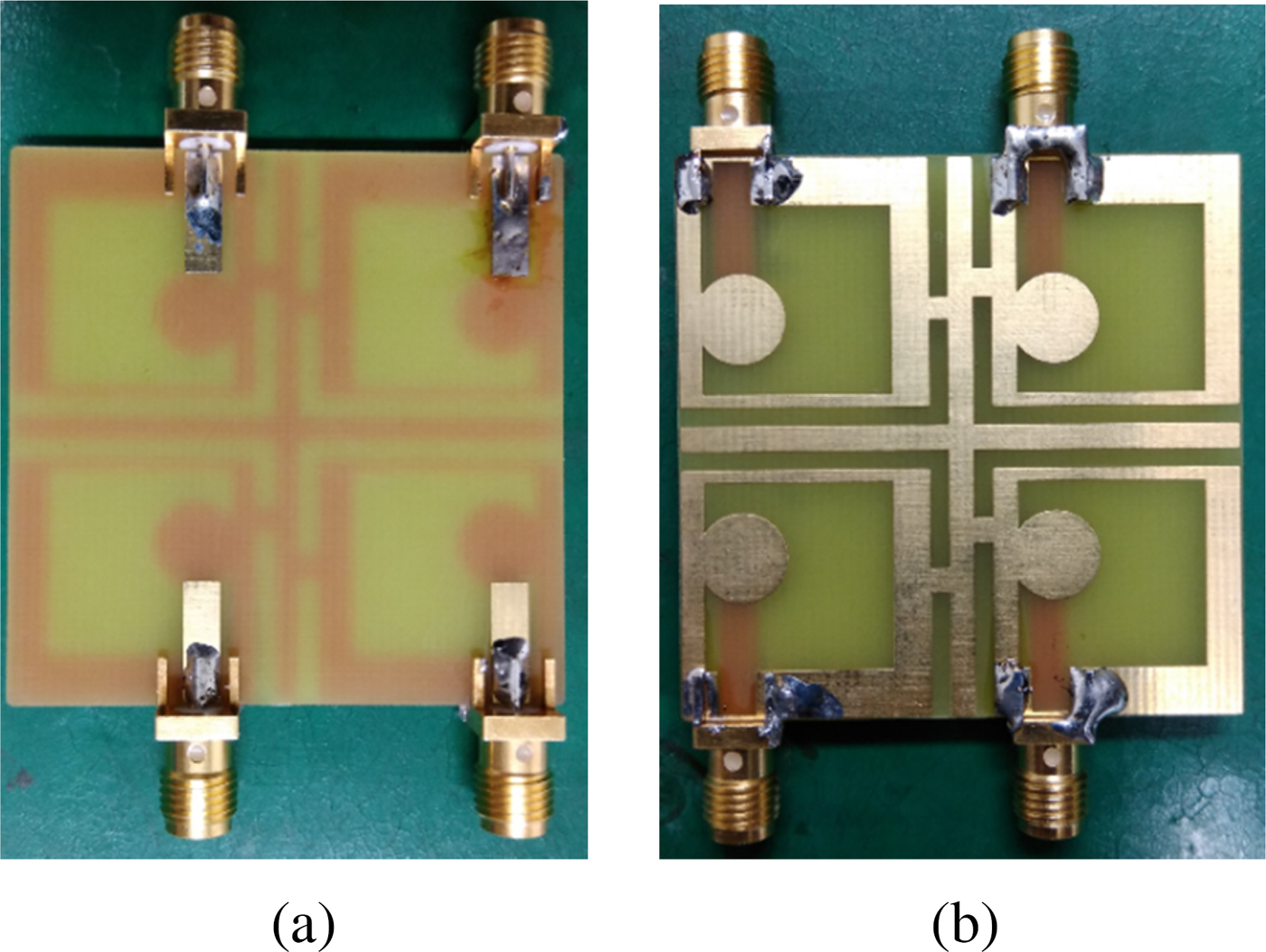
Fig. 11. Pictures of the fabricated four-element MIMO antenna: (a) front view and (b) rear view.
Results and discussion
The antenna performance parameters were measured using an Anritsu MS4644B vector network analyzer. The simulated and measured reflection coefficients of the proposed four-port MIMO antenna are shown in Fig. 12. It is observed that the antenna is operating in the band of 3.1–11 GHz (7.9 GHz), thus covering the complete UWB range. During the process of antenna measurements, one port of the MIMO antenna is excited and the other ports are terminated with the 50 Ω matched loads. The isolation level between different antenna elements is shown in Fig. 13, and it can be observed that isolation of more than 16 dB is provided between the various antenna ports. The axial ratio performance of the proposed MIMO antenna is shown in Fig. 14, and it is noticed that a good quality of circular polarization (4.8–6.9 GHz) is achieved in the band of interest. The axial ratio bandwidth can be increased further by introducing more spacing between the radiating elements. The utilization of complex decoupling structures also increases the circular polarization bandwidth. However, the overall MIMO antenna size will be increased in addition to the design complexity. The spacing and width of the strip are optimized so that a compact geometry (with minimum inter-element coupling and wide 3 dB axial ratio bandwidth) can be obtained.

Fig. 12. S-Parameters of the proposed four-element MIMO antenna.

Fig. 13. S-Parameters of the proposed four-element MIMO antenna with reference to (a) port-1 and (b) other ports.

Fig. 14. Axial ratio and gain of the proposed four-element MIMO antenna.
Figure 14 presents the simulated and measured gain characteristics of the antenna, and the antenna exhibits a peak gain of 5.5 dBi. The ECC for a four-port MIMO system (N = 4) between antenna elements i = 1 and j = 2 (Fig. 10) is expressed as [Reference Naji36]
 $$\rho _e(1,\; 2,\; 4) = \displaystyle{{{\left\vert {S_{11}^* S_{12} + \; S_{21}^* S_{22} + S_{13}^* S_{32} + \; S_{14}^* S_{42}} \right\vert}^2} \over \matrix{\left( 1-{\left\vert {S_{11}} \right\vert}^2-{\left\vert {S_{21}} \right\vert}^2-{\left\vert {S_{31}} \right\vert}^2-{\left\vert {S_{41}} \right\vert}^2} \right) \cr \left( {1-{\left\vert {S_{12}} \right\vert}^2-{\left\vert {S_{22}} \right\vert}^2-{\left\vert {S_{32}} \right\vert}^2-{\left\vert {S_{42}} \right\vert}^2 \right)} }$$
In a similar manner, the ECC between other antenna ports can be calculated by changing the values of i and j. Figure 15 illustrates the diversity performance of the proposed MIMO antenna, and it can be seen that the ECC is below 0.015 in the entire operating range of the antenna. The radiation patterns of the proposed antenna at 5.5, 6, and 6.5 GHz are shown in Fig. 16, and it can be observed from the presented plots that the antenna radiates LHCP waves. The simulated and measured results are in good agreement, and a small amount of difference is due to fabrication error and cable effects.

Fig. 15. ECC of the proposed four-element MIMO antenna.
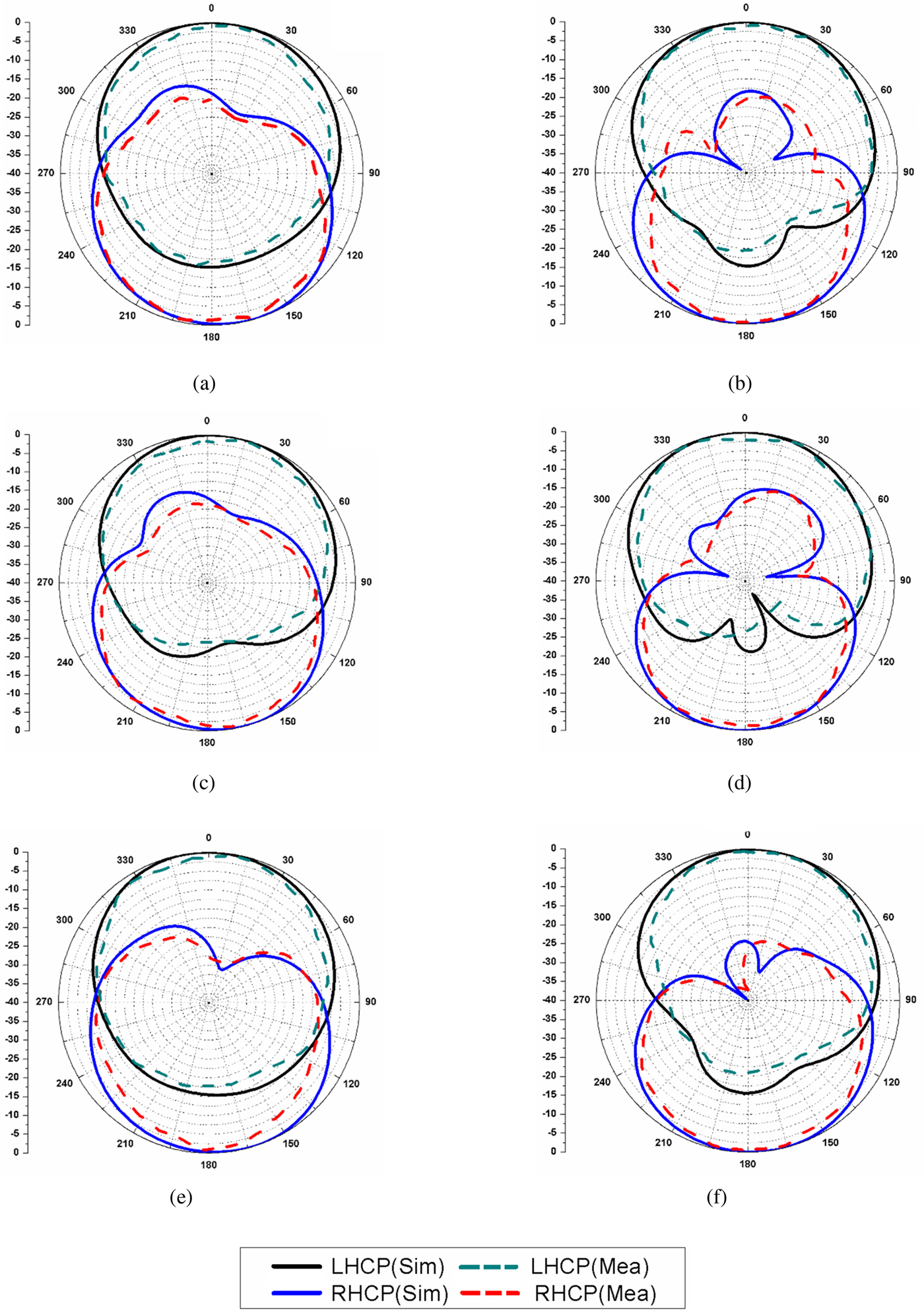
Fig. 16. Radiation patterns of the proposed antenna: (a) 5.5 GHz, ϕ = 0°, (b) 5.5 GHz, ϕ = 90°, (c) 6 GHz, ϕ = 0°, (d) 6 GHz, ϕ = 90°, (e) 6.5 GHz, ϕ = 0°, and (f) 6.5 GHz, ϕ = 90°.
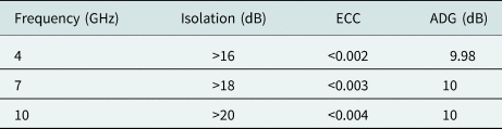
Further, the apparent diversity gain (ADG), which implies the increment in the quality of a signal owing to the introduction of diversity scheme in the MIMO systems, is also calculated [Reference Chandel, Gautam and Rambabu37]. For the proposed four-port MIMO antenna, the performance parameters at frequencies 4, 7, and 10 GHz are presented in Table 3, and it is observed that the value of ADG is more than 9.9 dB.
Table 3. Performance parameters of the proposed four-element UWB MIMO antenna
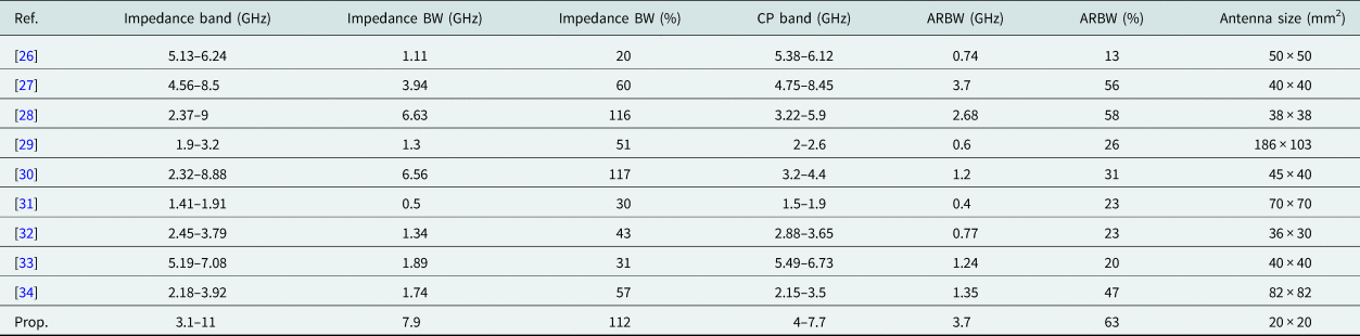
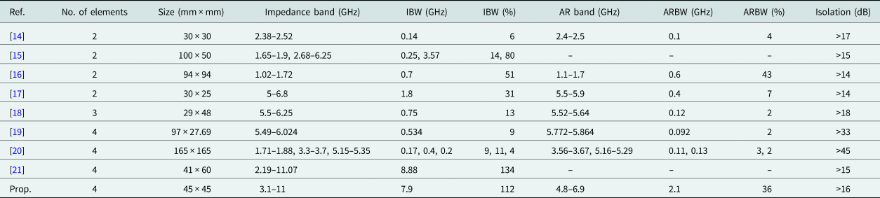
The comparison of the proposed four-port CP MIMO antenna with the other reported MIMO antenna structures is shown in Table 4 [Reference Qu, Piao and Qu14–Reference Kayabasi, Toktas, Yigit and Sabanci21]. The CP MIMO antennas reported in [Reference Qu, Piao and Qu14, Reference Yao, Wang, Chen, Yu and Liu16–Reference Sharma, Sarkar, Saurav and Srivastava18] are two- or three-port structures with relatively large size and small impedance bandwidth. In [Reference Yao, Wang, Chen, Yu and Liu16], the 3 dB axial ratio bandwidth is comparatively better, but the isolation between antenna elements is poor. The MIMO antennas reported in [Reference Malviya, Panigrahi and Kartikeyan19, Reference Parbat, Tambe, Kadu and Labade20] are four-port structures, but their impedance bandwidth and axial ratio bandwidth are very small. The MIMO antennas reported in [Reference Choukiker, Sharma and Behera15, Reference Kayabasi, Toktas, Yigit and Sabanci21] are linearly polarized. From the comparison, it can be noticed that the proposed MIMO antenna is compact in size covering a wide range of impedance and axial ratio bandwidth. Also, due to a planar geometry and common ground plane, the antenna can be easily integrated on a printed circuit board/MMICs.
Table 4. Comparison of the proposed antenna with other reported MIMO structures
IBW, impedance bandwidth; ARBW, axial ratio bandwidth.
Conclusion
In this work, a compact four-port UWB MIMO antenna with broadband circular polarization characteristics is presented. The proposed MIMO antenna is low-profile and simple to be designed, and also can be easily integrated with other microwave devices. The antenna provides an impedance bandwidth of 7.9 GHz and axial ratio bandwidth of 2.1 GHz. A plus-shaped conductor strip is used for connecting the ground planes of four antenna elements in order to ensure a common reference voltage level in the ground plane. The isolation, ECC, and ADG are within the acceptable limits, thus validating diversity performance of the MIMO antenna. Thus, the proposed four-port CP MIMO antenna with connected ground planes effectively deals with the shortcomings, which have been existed in the reported MIMO structures, and can be utilized for upper Wi-MAX, WLAN, and C-band applications.
Acknowledgement
This work was supported by the National Research Foundation (NRF) of Korea grant funded by the Korea Government (MSIT) (NRF-2018R1D1A3B07047848) and the BK21 Plus Project funded by the Ministry of Education, Korea (21A20131600011).
 Sachin Kumar received his B.Tech. degree in Electronics & Communication Engineering from Uttar Pradesh Technical University, Lucknow, India, in 2009. He received his M.Tech. and Ph.D. degrees in Electronics & Communication Engineering from Guru Gobind Singh Indraprastha University, Delhi, India, in 2011 and 2016, respectively. At present, he is working as a Post-Doctoral Researcher in the School of Electronics Engineering, Kyungpook National University, Daegu, Korea. His research interests include circularly polarized microstrip antennas, reconfigurable antennas, ultra-wideband antennas, defected ground structure, and microwave components.
 Gwan Hui Lee received his B.S. degree in Physics and Energy Sciences from Kyungpook National University, Daegu, Korea, in 2015, and received his M.S. degree in Electronics Engineering from Kyungpook National University, Daegu, Korea, in 2017. He is currently pursuing his Ph.D. degree in Electronics Engineering (specializing in Radio Communication Systems Engineering) in the Microwave Communications Laboratory, Kyungpook National University. His research interests include design and development of microwave circuits and wideband microwave passive components.
 Dong Hwi Kim received his B.S. degree in Electronic Engineering from Keimyung University, Daegu, Korea, in 2015. He received his M.S. degree in Electronics Engineering (major in Radio Communication Systems Engineering) from Kyungpook National University, Daegu, Korea, in 2017. He is currently pursuing his Ph.D. degree in Electronics Engineering (Radio Communication Systems Engineering) from Kyungpook National University. His fields of research include high-frequency filter design, frequency selective surface, passive devices, and waveguide antennas.
 Wahab Mohyuddin received his B.S. degree in Telecommunication Engineering from the National University of Computer & Emerging Sciences, Pakistan, in 2011, and received the M.S. and Ph.D. degrees in Electronics Engineering from Kyungpook National University, Daegu, Korea, in 2014 and 2018, respectively. He is currently working as a Post-Doctorate Researcher in Microwave Convergence Laboratory of Kyungpook National University. His research interests include design of RF/microwave/millimeter-wave circuits and systems designing, wideband microwave passive components, frequency selective surfaces, and microwave antennas.
 Hyun Chul Choi received his B.S. degree in Electronics Engineering from Kyungpook National University, Daegu, Korea, in 1982, and his M.S. and Ph.D. degrees in Electronics Engineering from the Korea Advanced Institute of Science and Technology (KAIST), Korea, in 1984 and 1989, respectively. In 1990, he joined Kyungpook National University as a Professor and is currently serving as Dean of the IT College. He has published numerous papers in the fields of EMI/EMC, scattering and propagation station, RF/microwave circuits and systems.
 Kang Wook Kim received his B.S. and M.S. degrees in Electrical Engineering from Seoul National University, Korea, in 1985 and 1987, respectively. He received his Ph.D. degree in Electrical Engineering from the University of California, Los Angeles, USA, in 1996. In 1987, before pursuing his Ph.D. degree, he worked as a Researcher at the Korea Electrotechnology Research Institute. He worked as a Design Engineer at P-Com Inc., USA and Narda DBS Microwave, USA, in 1998 and 1999, respectively. In 2001, he joined Kyungpook National University, Daegu, Korea, as a Professor. He is a founder of EM-wise Communications Company Inc., Korea. His areas of research include microwave communication systems and subsystems, microwave and millimeter-wave components and packaging, wireless communications, broadband microwave antennas, electromagnetic interaction and numerical analysis.


