


1. Introduction
Quasi-continuous wave (QCW) semiconductor lasers are efficient pump sources for high-power and short pulse laser systems. Such solid-state lasers or amplifier systems are primarily used for industrial macro- and micromachining, but they also cover a broad spectrum of scientific applications. For most of these applications several hundred watts up to several kilowatts pump power and high pulse energy out of an optical fiber are required. Customary high-power fiber coupled modules utilize passively cooled laser diode bars or actively cooled laser diode stacks with an emitting aperture of 10 mm. However, the use of standard bars requires complex beam-shaping techniques and a proper thermal and electrical management[Reference Treusch, Du, Baumann, Sturm, Ehlers and Loosen1–Reference Daiminger, Dorsch and Lorenzen5]. As more and more power out of the fiber is wanted and the need for higher brightness arises, designing such pump systems becomes a challenge, resulting in higher production as well as higher operating costs. Hence, new concepts for cost-effective fiber-coupling systems are needed to fulfill the increasing demands of future high-power pump applications.
We have presented a new approach based on a conduction cooled mini-bar design with 1.6 mm aperture width in Ref. [Reference Pittroff, Erbert, Eppich, Fiebig, Vogel and Tränkle6]. On the other hand, there is seen a huge potential in single emitter based systems since the performance of broad-area (BA) lasers has enormously increased in recent years[Reference Crump, Blume, Paschke, Staske, Pietrzak, Zeimer, Einfeldt, Ginolas, Bugge, Häusler, Ressel, Wenzel and Erbert7–Reference Yalamanchili, Rossin, Skidmore, Tai, Qiu, Duesterberg, Wong, Bajwa, Duncan, Venables, Verbera, Dai, Feve and Zucker11]. However, power scaling of BA lasers is limited due to filamentation, which downgrades their lateral beam quality and their reliability.
In this paper, we show a gain-guided stripe array with an aperture similar to that of a BA laser, which combines high pulse power and high beam quality, allowing efficient fiber coupling in the kW range without expensive beam reorganization. The emission wavelength of the laser is 940 nm.
The paper is structured as follows. The chip design is detailed in Section 2. In Section 3, laser diode packaging and the theoretically predicted thermal behavior of the laser device is described and shown to be consistent with experiment. Detailed measurement data for packaged devices are subsequently presented in Section 4. Finally, Section 5 reports on the reliability of the laser.
2. Chip design
2.1. Layer design
The vertical design of the laser chip is based on a super-large optical cavity (SLOC) structure with a thickness of  $3. 4~\mathrm{\mu} \mathrm{m} $. A large cavity affords the benefit that the optical intensity at the laser facet is diminished, which increases the level for catastrophic optical mirror damage (COMD) and consequently leads to a higher reliability of the laser chip. At the same time, the SLOC structure reduces the vertical far-field angle, resulting in a smaller beam height after collimation of the laser chip. By using micro-lenses with a longer focal distance, the alignment tolerances of the collimation lens are reduced.
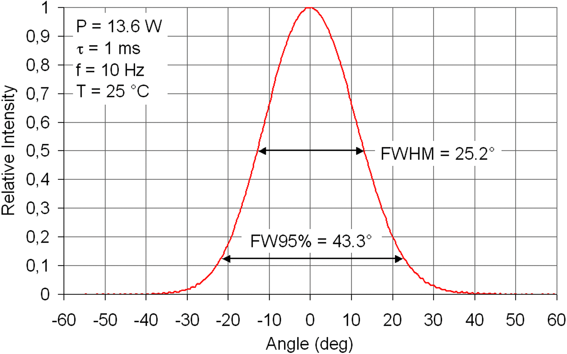
Figure 1 shows the Gaussian-shaped vertical far-field characteristic of the chip. The measured full width at half maximum (FWHM) divergence angle reaches 25.2° and the angle with 95% power included amounts to 43.3°.
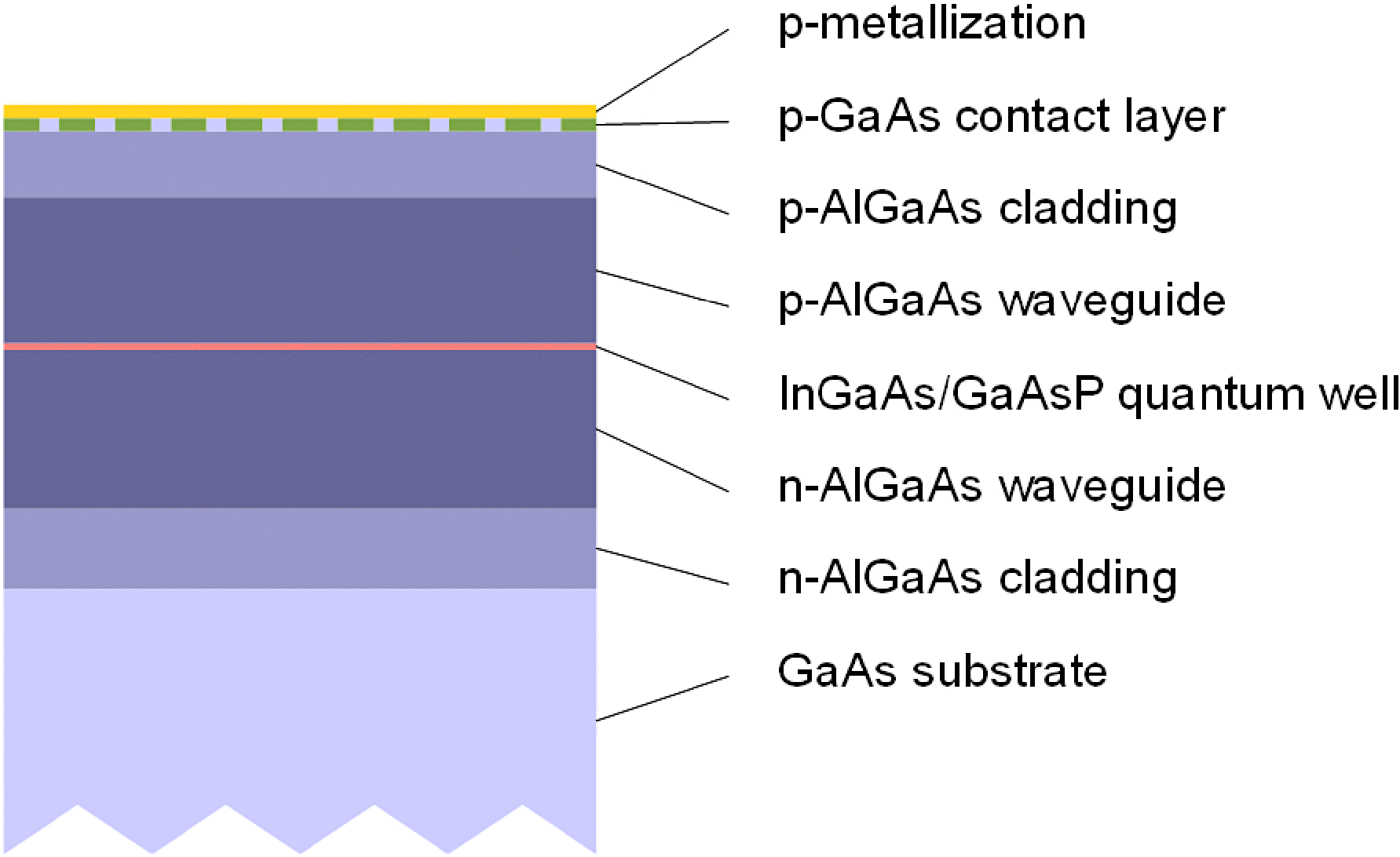
Figure 2 depicts the epitaxial arrangement of the chip. The layers were grown by low-pressure metal–organic vapor-phase epitaxy (MOVPE) on (100)-GaAs substrates. The active region comprises a compressively strained InGaAs quantum well (or wells) embedded in GaAsP barrier layers. Two variations have been fabricated: a structure with a single quantum well (SQW) and one with a double quantum well (DQW). The quantum well is surrounded by a  $2. 4~\mathrm{\mu} \mathrm{m} $ thick AlGaAs waveguide with low Al content and a thin AlGaAs cladding layer with high Al content. The thin cladding layers prevent generation of higher-order vertical modes. Both optimized Al concentration and layer thicknesses keep the series resistance small. The p contact layer is grown of highly doped GaAs.

Figure 1. Measured vertical far-field characteristic of the laser chip.
2.2. Chip layout
The chip layout is based on a narrow-stripe array with  $400~\mathrm{\mu} \mathrm{m} $ emitting aperture. Such a design allows a high output power in combination with a low lateral beam product. The stripe pattern was formed by selective implantation of He+ ions into the GaAs contact layer, which cause a decrease of the electrical conductivity. For lateral wave guiding, index grooves were etched adjacent to the array. Additionally, V-grooves are incorporated to prevent rival transverse or ring modes.
Figure 2. Schematic cross-sectional view of the semiconductor structure.
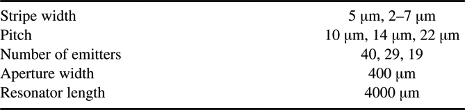
We processed different lateral structures by a variation of the stripe geometry and the emitter spacing (pitch  $p$) (Table 1). Two stripe geometries have been investigated: standard (rectangular) stripes with a stripe width $w$ of $5~\mathrm{\mu} \mathrm{m} $ and slightly tapered stripes with $w= 2~\mathrm{\mu} \mathrm{m} $ at the back facet and $w= 7~\mathrm{\mu} \mathrm{m} $ at the front facet. From the tapered stripe we expected higher lateral modes to be less likely to occur, which might result in a better beam quality. Arrays with 19, 29 and 40 emitters were made, each with $400~\mathrm{\mu} \mathrm{m} $ aperture, resulting in a different pitch.
The chip exhibits a 4 mm long cavity affording a high optical power in combination with low serial and thermal resistance values. The reflectivity at the front facet varied between 1.5% and 3.1%, and the reflectivity at the rear facet was 95%. A facet passivation with ZnSe as described in Ref. [Reference Ressel, Erbert, Zeimer, Häusler, Beister, Sumpf, Klehr and Tränkle12] had been applied prior to the coating process.
Table 1. Investigated chip layouts
3. Diode laser package
3.1. Heat sink and chip mounting
Figure 3 depicts the complete laser device. The laser chips were mounted p-side down onto 0.4 mm thin, passively cooled, aluminum nitride (AlN) submounts using AuSn solder. The top and the bottom side of the AIN substrate is plated with  $50~\mathrm{\mu} \mathrm{m} $ thick copper, for electrical (upper surface) and thermal contacting. The copper layer is finished with Ni/Au, and AuSn solder is applied to the p side by vapor deposition.
Copper-plated AlN heat sinks are increasingly used in the semiconductor laser industry. There are four main reasons.
(1) AlN in combination with copper has a resulting coefficient of thermal expansion (CTE) which is nearly the same as the CTE of GaAs: $\mathrm{CTE} = 6. 5\times 1{0}^{- 6} / {\unicode{x00B0}} \mathrm{C} $.
(2) The thick copper layer at the heat source reduces the thermal resistance (
${R}_{th} $) of the laser.(3) Besides, it increases the current-carrying capacity.
(4) AlN ceramics is relatively inexpensive.

These properties allow for optimal chip mounting and for cost-effective manufacture.
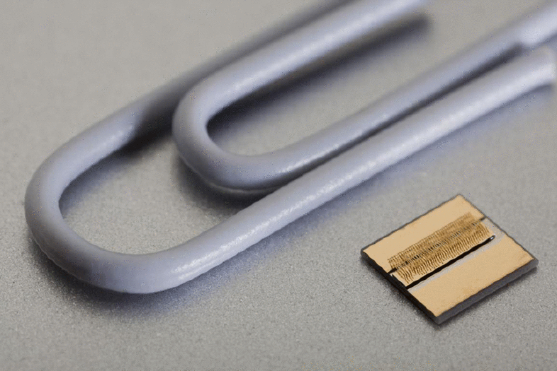
Figure 3.  $400~\mathrm{\mu} \mathrm{m} $ high-power QCW laser for kW-pump modules. The chip is mounted on a plated AlN substrate. The size of the submount is $4~\mathrm{mm} \times 4. 5~\mathrm{mm} \times 0. 4~\mathrm{mm} $.
Since a pump module will contain a few tens of laser chips, which all must be of the same quality and of constant alignment in order to achieve a high coupling efficiency into the optical fiber, high-precision mounting is required. Hence, the chips were mounted fully automated using a ficonTEC BL2000 high-performance bonding system, which has been designed for industrial manufacture as well as for high placement accuracy. Thus, a placement accuracy of  $\pm 5~\mathrm{\mu} \mathrm{m} $ in the lateral direction of the chip could be attained. After the soldering process the n side of the chip was connected to the submount using fine pitch wire bonding technology with gold wires. This process has been automated as well.
3.2. Thermal simulation
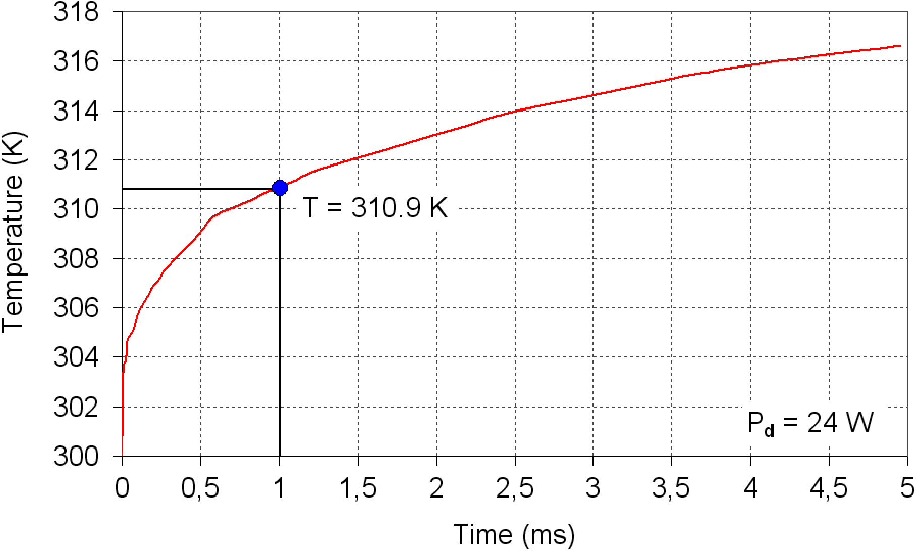
The laser device was designed for QCW operation with a pulse duration of 1 ms. The performance of the diode laser in the presence of current heating is strongly influenced by the temperature of the active region, also termed junction temperature. During the long pulses junction temperature will increase, leading to longer wavelength. In order to determine the expected temperature distribution and the temperature rise, a dynamic thermal simulation for the  $5~\mathrm{\mu} \mathrm{m} / 14~\mathrm{\mu} \mathrm{m} $ array was done by means of the finite-element software MSC NASTRAN/PATRAN. The simulation was performed with a dissipation power ${P}_{d} $ of 24 W, corresponding to a pulse power of 35 W (nominal power). It was assumed that there is no temperature dependence in the material parameters.
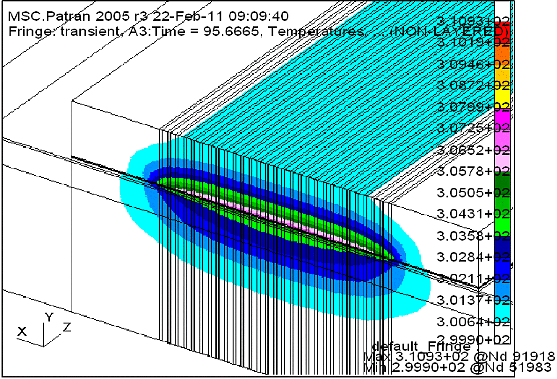
The calculated temperature distribution after 1 ms pulse operation and the simulated temperature transient are depicted in Figures 4 and 5, respectively. The temperature of the AlN heat sink was kept at  $T= \mathrm{const.} = 300~\mathrm{K} $. With the above parameters we reach a maximum temperature rise of 10.9 K in the center of the emitting aperture. Due to the thick copper layer the dissipated power is efficiently cooled away from the chip. The heat expansion is limited to a small region around the array and only marginally reaches the substrate. Note that the temperature transient is dependent on the dissipation power. The higher it is, the higher will be the temperature rise as well.
Figure 4. Simulated temperature distribution at the front facet after 1 ms pulse operation and at a dissipation power of 24 W. The laser reaches a maximum temperature rise of 10.9 K in the central emitter.
Figure 5. Calculated variation of junction temperature with time (transient analysis) for the  $5~\mathrm{\mu} \mathrm{m} / 14~\mathrm{\mu} \mathrm{m} $ laser chip mounted on an AlN submount.
In order to allow a direct comparison with experiment, one can determine the thermal resistance  ${R}_{th} = \mathrm{\Delta} T/ {P}_{d} $ of the assembly by specifying a dissipation power of 1 W and calculating the heating $ \mathrm{\Delta} T$ in the CW case (here, taken as the heating predicted for pulse length of 5 ms, where the temperature saturates). Depending on the position of the emitter we obtain a temperature rise in the range of 0.6–0.8 K. Hence, we can deduce a maximum ${R}_{th} $ of 0.8 K/W and a mean ${R}_{th} $ of 0.7 K/W, which is in exact agreement with the ${R}_{th} $ calculated from our measurements (see Section 4.2).
It should be kept in mind that the heating of the active region during each single pulse leads to a corresponding drift of the emission spectrum (‘thermal chirp’), which will result in a spectral broadening. At the end of the pulse the temperature difference between the laser chip and the heat sink lies between 7 K (outer emitters) and 10.9 K (central emitter). The wavelength temperature coefficient of the chip is 0.31 nm/K. Thus, we expect a spectral broadening between 2.2 and 3.4 nm (see Section 4.2).
4. Measurement results
For detailed measurements the lasers devices were clamped onto a special measurement mount, which was mounted onto a heat sink with  $T= \mathrm{const.} = 25{\unicode{x00B0}} \mathrm{C} $. All measurements were performed with a pulse length of 1 ms. To minimize the mean dissipation power and thus to keep the temperature difference between the measurement mount and the AlN heat sink small, we used a repetition rate of 10 Hz (1% duty cycle). The series resistance of the measurement setup was subtracted in the following light–current–voltage (LIV) data.
4.1. Light–current–voltage characteristic
4.1.1. SQW–DQW influence
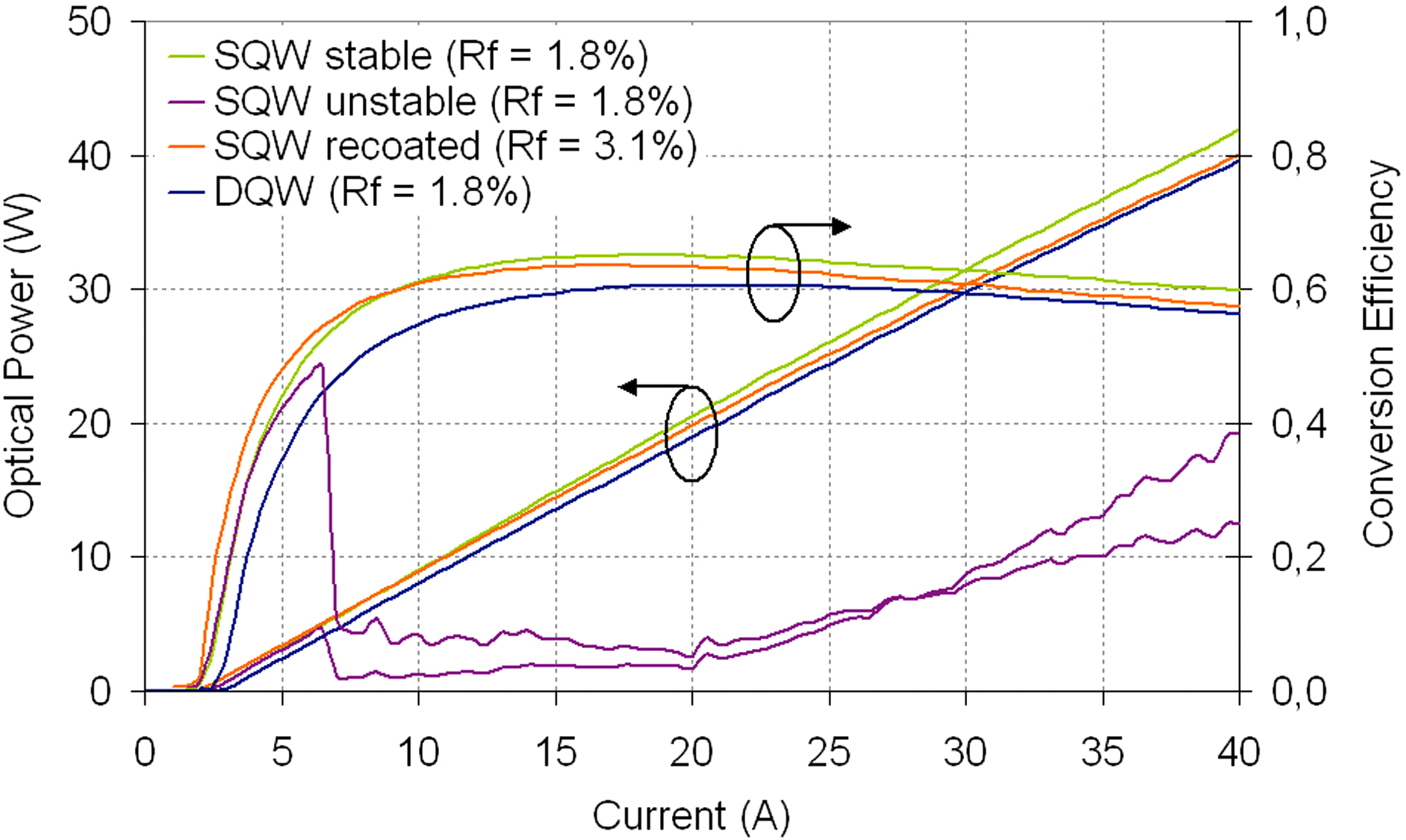
The typical dependence of the electro-optical characteristic of the laser device on the quantum well is shown in Figure 6 for the example of the  $2{\unicode{x2013}} 7~\mathrm{\mu} \mathrm{m} / 14~\mathrm{\mu} \mathrm{m} $ chip layout which shows integrated optical output power and power conversion efficiency as a function of current. The power conversion efficiency, ${\eta }_{E} $, is defined as the ratio of optical output power, ${P}_{out} $, to the electrical input power supplied directly to the chip on submount. Specifically, ${\eta }_{E} = {P}_{out} / IV$, where $I$ is the operation current and $V$ is the voltage dropped across the input connections to the submount. Values of ${\eta }_{E} $ can be used to calculate the electrical input power necessary to achieve a target value of ${P}_{out} $. The SQW structure exhibits a higher slope efficiency ( $S= 1. 13$ W/A) and a smaller threshold current ( ${I}_{th} = 2. 38$ A) than the DQW structure ( $S= 1. 08$ W/A, ${I}_{th} = 2. 85$ A), but it revealed unstable operation. It turned out that the SQW laser, although comprising V-grooves, tends to ring modes. Such ring modes arise from multiple total reflections at the laser facets and the lateral boundaries of the active layer and are competing against the longitudinal laser modes. To diminish the losses of the laser modes, the front-facet reflectivity of the SQW chips was increased to ∼3%. Recoating caused a decrease of slope efficiency from 1.13 W/A to 1.08 W/A, but it also decreased the threshold current ( ${I}_{th} = 1. 97$ A). Hence, at nominal output power ( ${P}_{nom} = 35$ W), the operating current of the recoated SQW chip ( ${I}_{nom} = 34. 5$ A) is smaller than that of the DQW chip ( ${I}_{nom} = 35. 0$ A). The conversion efficiency at ${P}_{nom} $ reaches 59.2% (SQW) and 57.9% (DQW). The maximum conversion efficiency is 63.6% (SQW) and 60.6% (DQW).
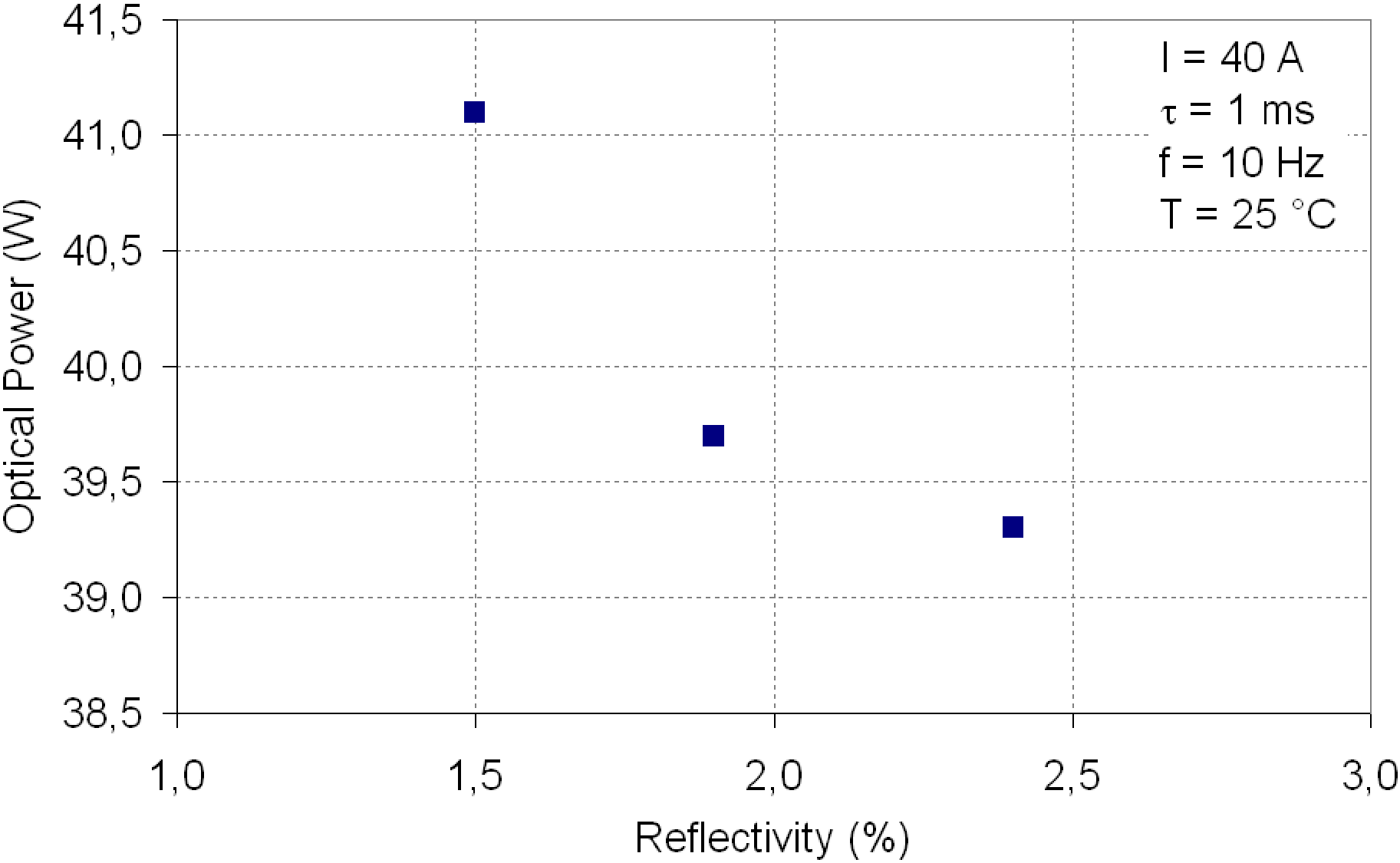
Due to several coating runs, the reflectivity of the laser facet varied between 1.5% and 2.4% (DQW), which had a slight influence on the electro-optical performance of the laser. From a series of measurements we observed that a decrease of reflectivity from 2.4% to 1.5% gave an increase in the output power of ∼5% (Figure 7). At the same time the threshold current increased by 0.1 A.
Figure 6. LI characteristic ( $\tau = 1$ ms, $f= 10$ Hz, $T= 25{\unicode{x00B0}} \mathrm{C} $) of the SQW and DQW structures ( $w= 2{\unicode{x2013}} 7~\mathrm{\mu} \mathrm{m} $, $p= 14~\mathrm{\mu} \mathrm{m} $).
Figure 7. Output power of the  $2{\unicode{x2013}} 7~\mathrm{\mu} \mathrm{m} / 14~\mathrm{\mu} \mathrm{m} $ DQW array at 40 A as a function of the front-facet reflectivity.
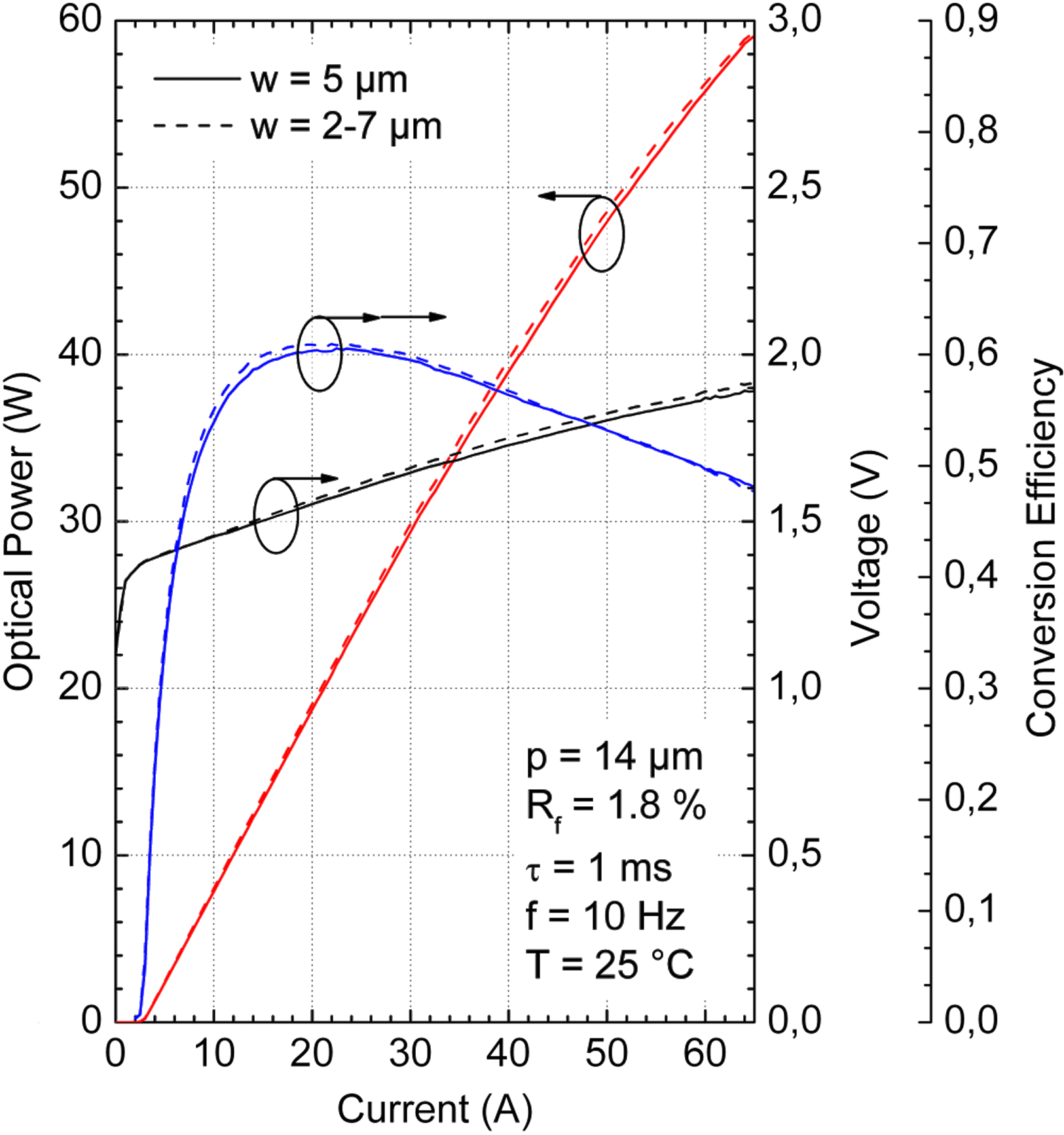
4.1.2. Influence of a tapered stripe
The influence of a slight taper is depicted in Figure 8. The plot shows that there is no significant difference between the two stripe geometries. Though, averaged across a large number of samples, little more optical power from the 2–7  $\mathrm{\mu} \mathrm{m} $ stripes could be found. Compared to the standard geometry ( $S= 1. 08$ W/A), the tapered stripe exhibits a slightly higher slope efficiency ( $S= 1. 1$ W/A). However, both geometries have shown the same threshold current ( ${I}_{th} = 2. 85$ A). The maximum conversion efficiency reached 60.6% at 22.5 A ( $w= 5~\mathrm{\mu} \mathrm{m} $) and 61.0% at 22 A ( $w= 2{\unicode{x2013}} 7~\mathrm{\mu} \mathrm{m} $). But since the structure with the tapered stripe has a little higher forward voltage, the conversion efficiency drops slightly at higher currents.
Figure 8. LIV curve of the DQW structure with  $14~\mathrm{\mu} \mathrm{m} $ pitch.
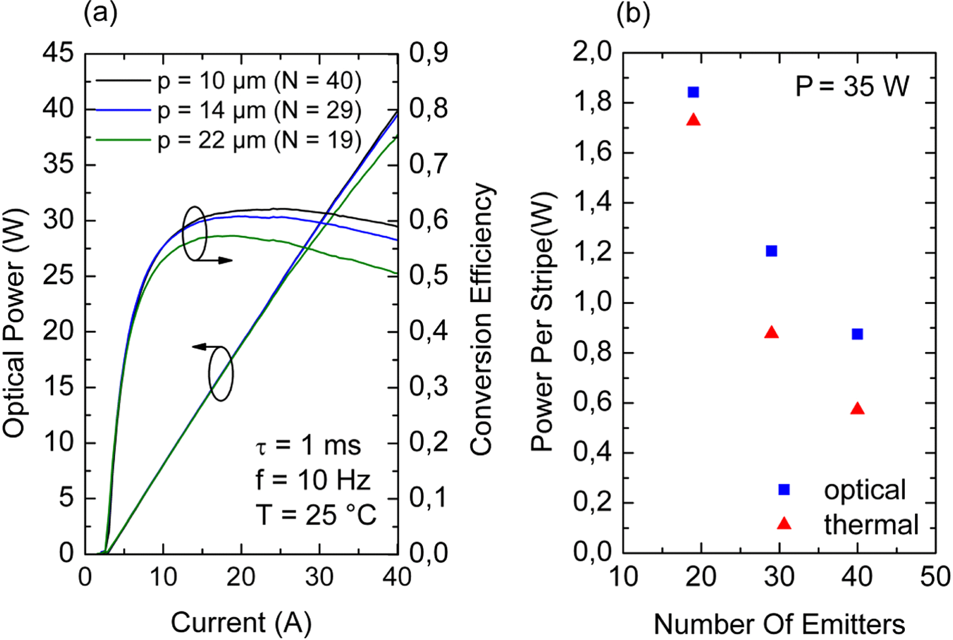
4.1.3. Influence of the pitch
The influence of the number of emitters integrated into the  $400~\mathrm{\mu} \mathrm{m} $ aperture on the light–current characteristic is exemplarily shown for the DQW laser with $w= 2{\unicode{x2013}} 7~\mathrm{\mu} \mathrm{m} $ in Figure 9(a). The best performance was achieved for $10~\mathrm{\mu} \mathrm{m} $ pitch (40 emitters). The 29-emitter structure reaches nearly the same output power as the 40-emitter structure, but the power conversion efficiency falls due to an increase of the series resistance. In addition, the higher pitch leads to an increase of the thermal resistance, which becomes evident at the 19-emitter structure by the onset of a thermal rollover.
Figure 9(b) depicts the optical power and the thermal load per stripe for 35 W optical output from the chip. The dissipation power per stripe of the 19-emitter array reaches 1.7 W, which is nearly three times the value of the 40-emitter array ( ${P}_{d} = 0. 6$ W/stripe).
Figure 9. (a) Measured LI characteristic dependent on the emitter pitch (number of emitters) and (b) corresponding plot of the optical/dissipation power per stripe against the number of emitters at 35 W overall optical power.
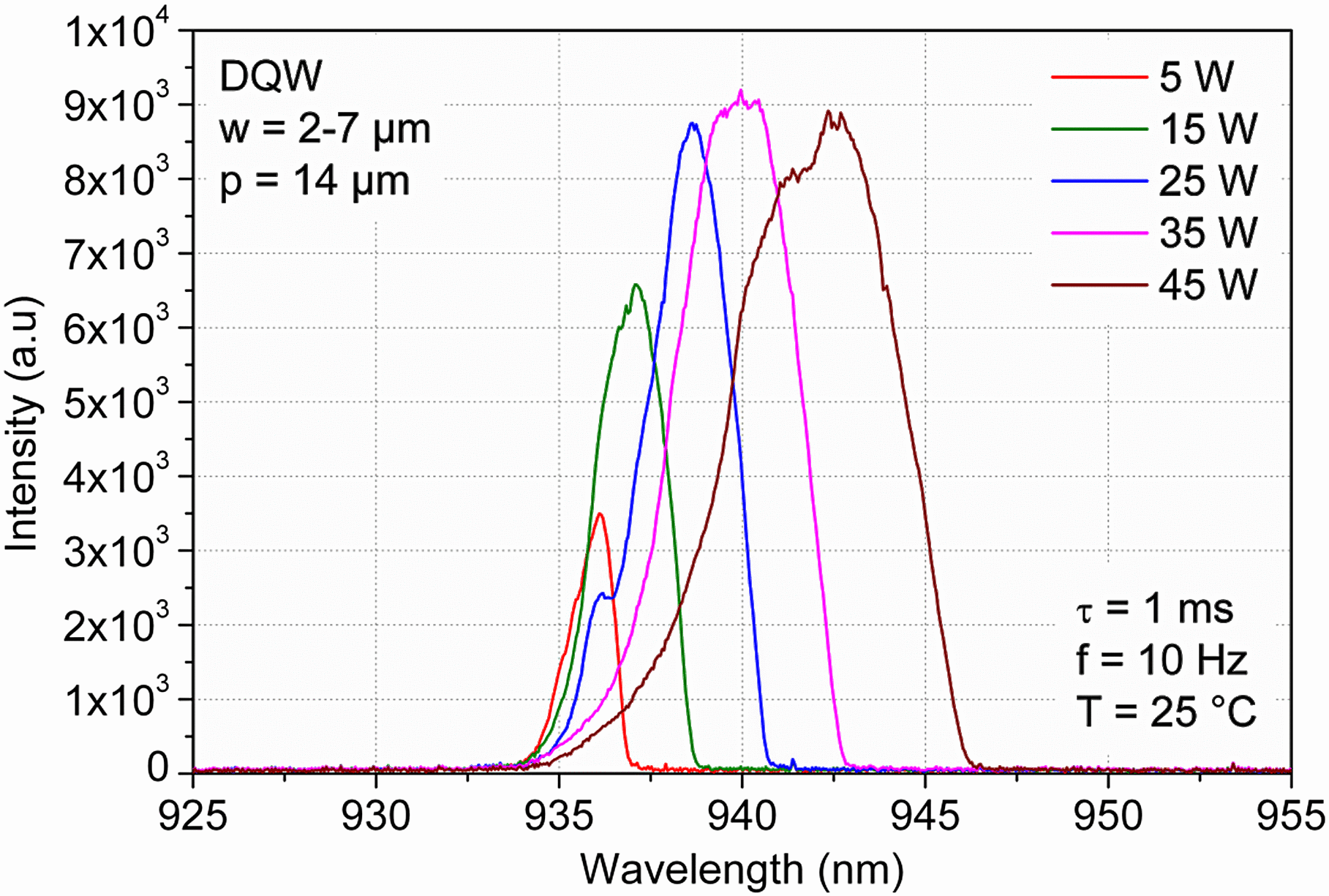
4.2. Spectral characteristic
Figure 10 shows the spectral characteristic of the  $14~\mathrm{\mu} \mathrm{m} $ pitch DQW structure at $T= 25{\unicode{x00B0}} \mathrm{C} $. At $P= 35$ W ( $\tau = 1$ ms, $f= 10$ Hz) the center wavelength is 939.9 nm. 95% spectral width is 6.2 nm and FWHM 3.8 nm, typically. Note that the emission wavelength can be changed by changing the indium content of the quantum well and the working temperature. By measuring the wavelength against temperature ( ${P}_{d} = \mathrm{const.} $) one gets the wavelength temperature coefficient $ \mathrm{\Delta} \lambda / \mathrm{\Delta} T$ of the laser, which is a material constant. We measured a $ \mathrm{\Delta} \lambda / \mathrm{\Delta} T$ of 0.31 nm/K. Using the wavelength temperature coefficient, we can calculate the ${R}_{th} $ of the laser by
 $${R}_{th} = \frac{ \mathrm{\Delta} T}{ \mathrm{\Delta} {P}_{d} } = {\left.\frac{ \mathrm{\Delta} \lambda }{ \mathrm{\Delta} {P}_{d} } \right\vert }_{T= \mathrm{const.} } \cdot {\left.{\left(\frac{ \mathrm{\Delta} \lambda }{ \mathrm{\Delta} T} \right)}^{- 1} \right\vert }_{{P}_{d} = \mathrm{const.} } ,$$
 where  $ \mathrm{\Delta} \lambda / \mathrm{\Delta} {P}_{d} $ is the wavelength shift over the change of dissipation power ${P}_{d} (I)= U(I)\cdot I- P(I)$, calculated from a CW measurement of the wavelength against drive current and the LIV data. With $ \mathrm{\Delta} \lambda / \mathrm{\Delta} {P}_{d} = 0. 216$ nm/W, we obtain an ${R}_{th} $ of 0.7 K/W, which is fully consistent with our simulation in Section 3.2. It was noted in Section 3.2 that the spectrum is broadened as a result of a thermal chirp. The broadening increases with higher dissipation power. For comparison, the spectral width (95% optical power included) measured close to the laser threshold ( $I= 3$ A) is 1.8 nm. Since there is no significant temperature increase up to threshold current, the broadening will be negligible. The difference between the spectral width at $P= 35$ W and the spectral width at threshold reveals an overall broadening of 4.4 nm. We expect that ∼3 nm comes from the thermal chirp. The remaining $ \mathrm{\Delta} \lambda = 1. 4$ nm is attributed to the inhomogeneous spatial temperature distribution along the emitters. Hence, we can estimate a mean temperature difference $ \mathrm{\Delta} T$ over the chip by $ \mathrm{\Delta} T= \mathrm{\Delta} \lambda / (0. 31~\mathrm{nm} / \mathrm{K} )= 4. 5$ K.
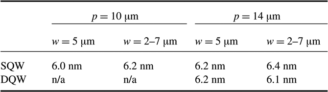
Table 2 compares the spectral broadening of the 10 and  $14~\mathrm{\mu} \mathrm{m} $ pitch samples. There were no significant differences observed between the vertical and lateral structures.
Figure 10. Spectral characteristic of the device for different optical power levels. The spectrum is broadened due to a thermal chirp.
Table 2. 95% spectral width at  $P= 35$ W ( $\tau = 1$ ms, $f= 10$ Hz) and $T= 25{\unicode{x00B0}} \mathrm{C} $
4.3. Lateral beam characteristic
The lateral near- and far-field distributions were measured by using the moving-slit technique. Detailed investigation of the beam characteristics of gain-guided arrays has been reported in Refs. [Reference Spreemann, Wenzel, Eppich and Erbert13,Reference Spreemann, Eppich, Schnieder, Wenzel and Erbert14].
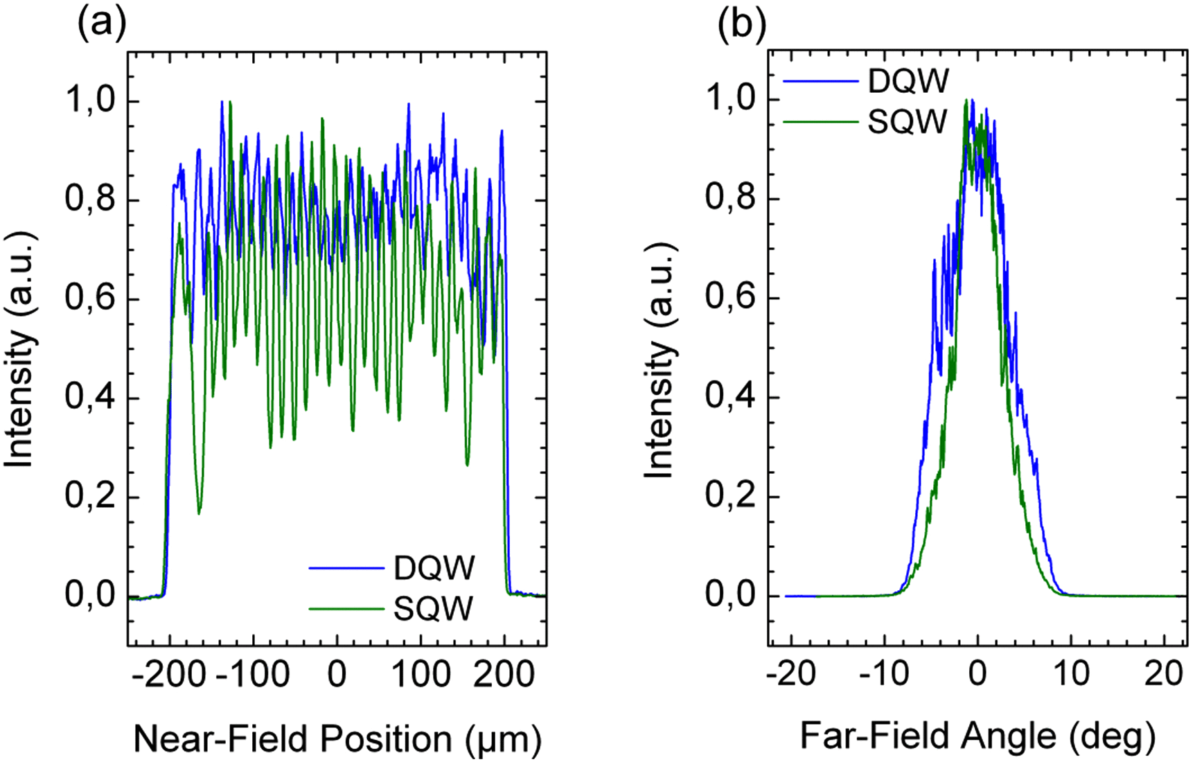
The typical near- and far-field profiles of both SQW and DQW structures with  $14~\mathrm{\mu} \mathrm{m} $ pitch and at 35 W optical power are depicted in Figures 11(a) and 11(b), respectively. For both vertical structures we obtain a nearly symmetrical single-lobe far-field distribution. The irregular near-field profile of the DQW structure indicates partial coherence of the single stripes, whereas the near-field distribution of the SQW laser shows nearly incoherent superposition of the stripe modes resulting in a Gaussian-like far-field. The lateral far-field angles with 95% power enclosed were typically 11.5° (SQW) and 13.5° (DQW), corresponding to a lateral beam parameter product (BPP) of 20.1 mm-mrad and 23.6 mm-mrad, respectively. Such low values are necessary for simple and cost-efficient multimode fiber coupling.
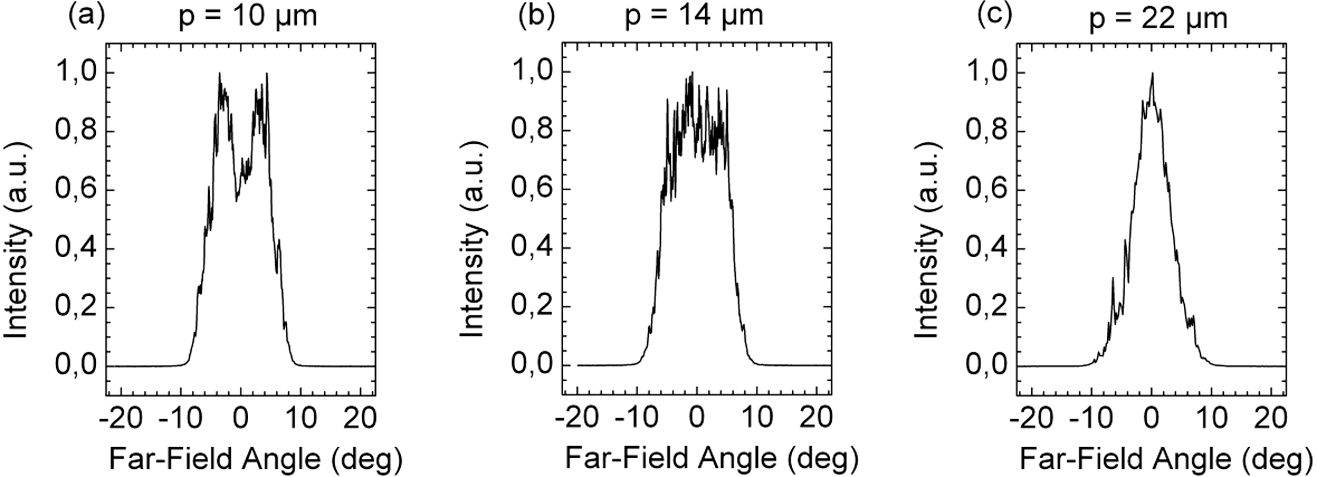
Figure 12(a–c) shows the far field of the DQW structure against the emitter pitch. Figure 12(a) shows a typical double-lobed intensity profile resulting from a superposition of so-called array modes. Such a distribution has also been observed for the  $14~\mathrm{\mu} \mathrm{m} $ pitch samples operating at an output power ${\lt }30$ W (not depicted here). In contrast, the SQW structure did not show a distinctive double lobe. Increasing the pitch minimizes coupling of the stripes. In Figure 12(c) no more coupling occurs, leading to a Gaussian-like profile. However, our measurements showed that the change in the far-field distribution did not affect the 95%-divergence angle. There were also no measurable differences apparent in the intensity profiles and the far-field angles between the $5~\mathrm{\mu} \mathrm{m} $ and the $2{\unicode{x2013}} 7~\mathrm{\mu} \mathrm{m} $ stripes.
Figure 11. Lateral (a) near- and (b) far-field profiles of the DQW and SQW laser at 35 W output power ( $\tau = 1$ ms, $f= 10$ Hz, $T= 25{\unicode{x00B0}} \mathrm{C} $).
Figure 12. Dependence of the lateral far-field of the DQW structure on the emitter pitch at  $P= 35$ W ( $\tau = 1$ ms, $f= 10$ Hz, $T= 25{\unicode{x00B0}} \mathrm{C} $).
5. Reliability tests
5.1. COD test
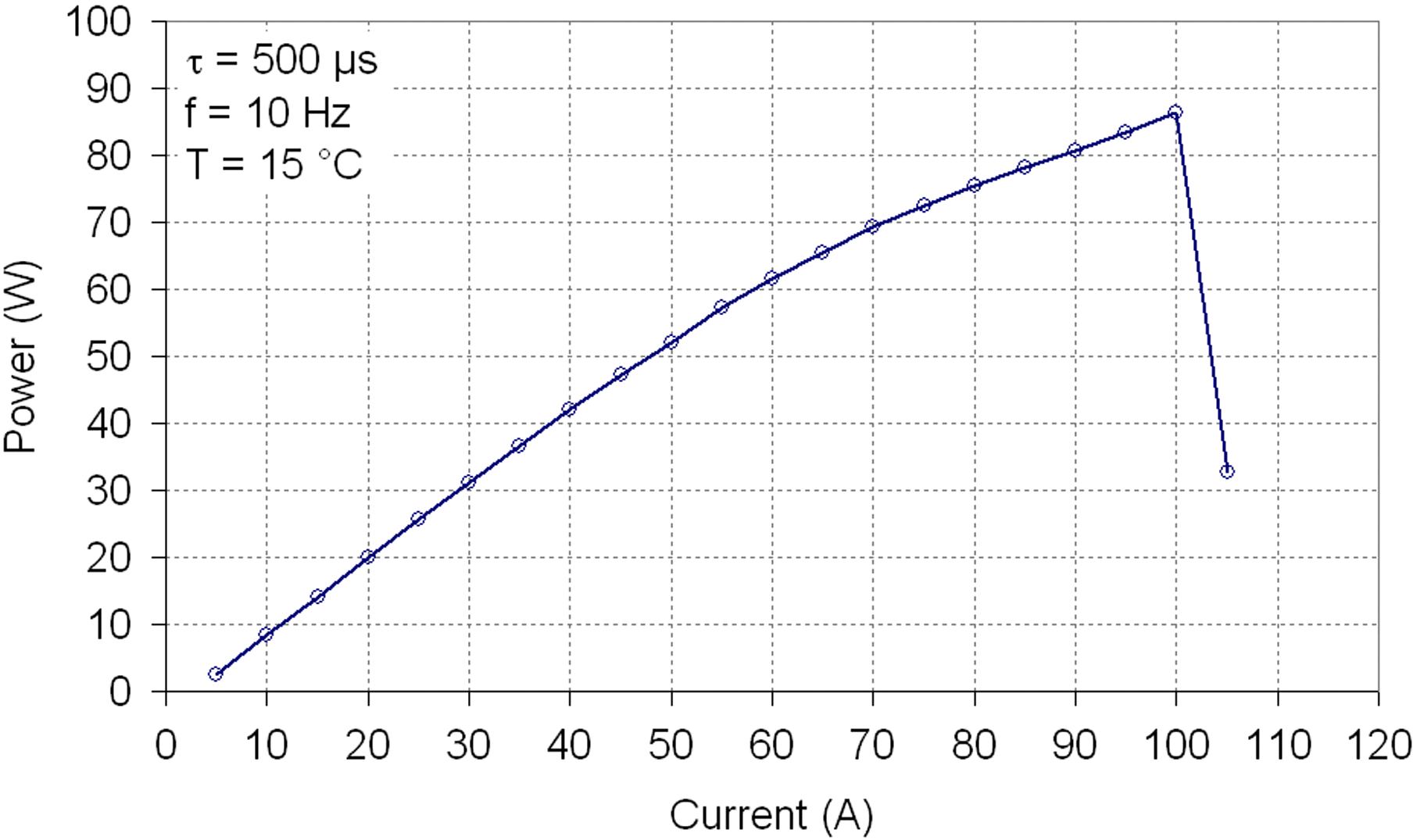
We examined the facet stability of the laser chip by performing a maximum power test with the  $2{\unicode{x2013}} 7~\mathrm{\mu} \mathrm{m} / 14~\mathrm{\mu} \mathrm{m} $ DQW structure ( ${R}_{f} = 1. 5\% $), where we measured the catastrophic optical damage (COD) level. (Figure 13). In order to avoid excessive heating of the chip, the laser was driven with $500~\mathrm{\mu} \mathrm{s} $ pulses and 1% duty cycle at $T= 15{\unicode{x00B0}} \mathrm{C} $. The laser reached a maximum power of 86 W at 100 A, which corresponds to 3 W optical power from one single stripe. Optical inspection and viewing the electroluminescence at the laser facet revealed no mirror damage. By means of cathodoluminescence imaging it could be detected that the laser failed due to an internal COD.
Figure 13. COD test. Chip structure: DQW,  $w= 2{\unicode{x2013}} 7~\mathrm{\mu} \mathrm{m} $, $p= 14~\mathrm{\mu} \mathrm{m} $.
5.2. Burn-in screening
Usually, during the first 100 hours of laser diode operation, failures due to rapid degradation can be observed. Rapid degradation is caused by intrinsic defects in the active region and is often a consequence of errors in the production process. To minimize the risk for rapid failures all lasers were subjected to an 168 hours burn-in screening. The screening was performed as follows. First a measurement at  $I= 40$ A ( $\tau = 1$ ms, $f= 10$ Hz, $T= 25{\unicode{x00B0}} \mathrm{C} $) was done in order to sort out lasers with a serious failure. Lasers that reached less than their typical pulse power ${P}_{typ} $ minus a fixed tolerance $ \mathrm{\Delta} {P}_{tol} = 1$ W were rejected. Subsequently, those lasers that passed the screening were burned at $I= 36$ A ( $\tau = 1$ ms, $f= 15$ Hz), corresponding to 35 W optical power. After the burn-in each laser was measured once again at $I= 40$ A. If a laser failed $(P\lt {P}_{typ} - \mathrm{\Delta} {P}_{tol} )$ it was also rejected.
We burned a total of 970 lasers with a yield of nearly 99%. It could be observed that all 960 lasers passing the burn-in showed no degradation.
5.3. Aging test
An aging test with a total of 43 lasers (25 DQW and 18 SQW lasers) with  $p= 14~\mathrm{\mu} \mathrm{m} $ was performed at constant current regime ( $I= 336$ A, $\tau = 1$ ms, $f= 15$ Hz) and at a laser diode mount temperature of 18°C after a successful burn-in screening.
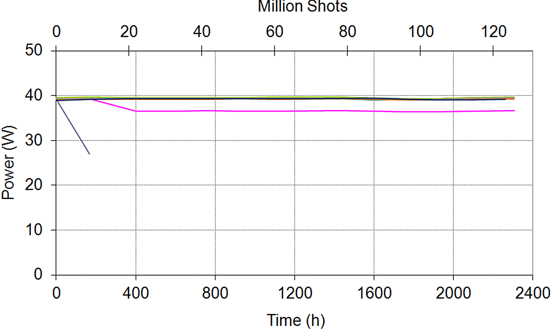
The optical output power versus operation time for the DQW lasers is given in Figure 14. Except for two lasers, all lasers showed stable operation over 2300 hours (124 million shots). One of the failed lasers showed a quick degradation within the first 200 hours. By viewing the laser facet we observed a coating defect. The second defective laser degraded between the first 200 and 400 hours, but then remained stable until the end of the test. Optical inspection revealed contaminations at the laser facet arising from the manufacturing process. The results may indicate that the burn-in conditions should be improved to better screen out early failures.
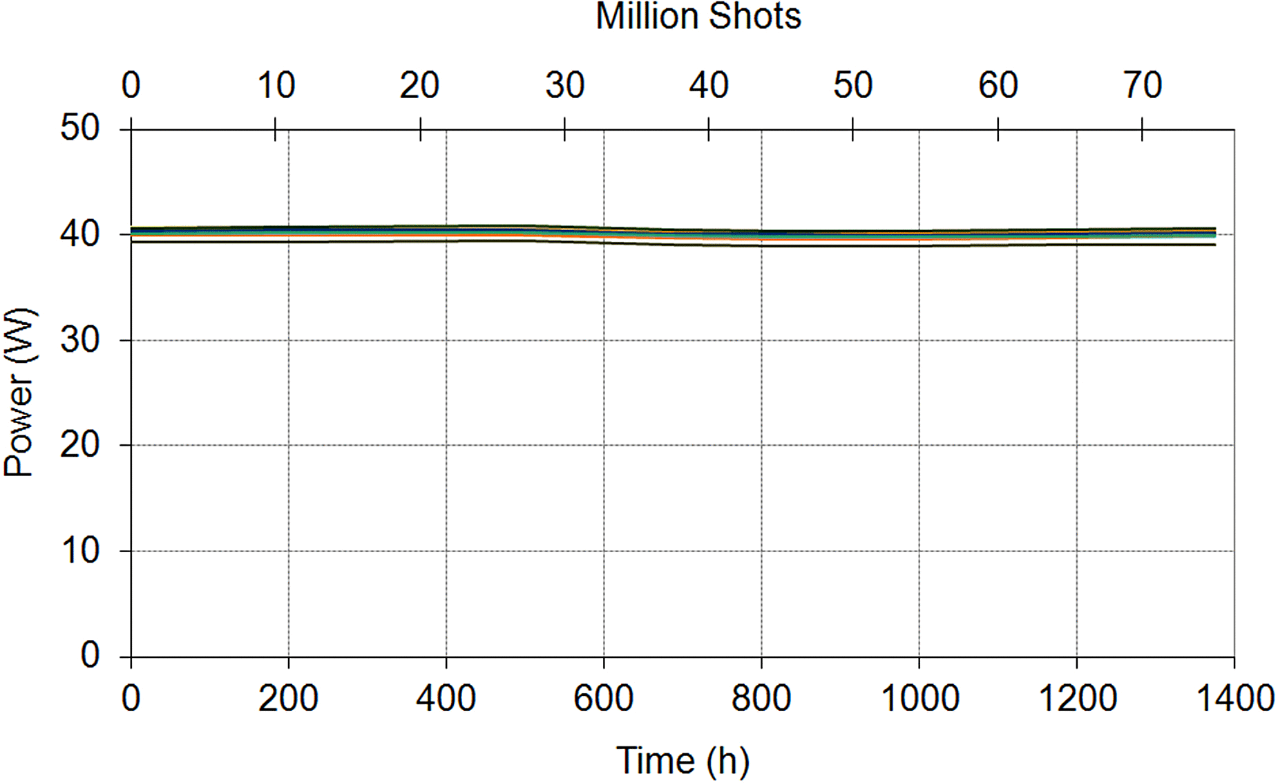
Figure 15 shows the optical power versus operation time for the SQW lasers  $({R}_{f} = 3. 1\% )$. After 1375 hours (74 million shots) of operation no degradation was observed.
Even though the tests allow no conclusions to be drawn about the expected life time, the results show that the laser device has the potential to serve as a building block in highly reliable applications.
Figure 14. Aging test of 25 DQW lasers after burn-in ( $I= 36$ A, $\tau = 1$ ms, $f= 15$ Hz). Measurement: $I= 40$ A, $t= 1$ ms, $f= 10$ Hz.
Figure 15. Aging test of 18 SQW lasers after burn-in ( $I= 36$ A, $\tau = 1$ ms, $f= 15$ Hz). Measurement: $I= 40$ A, $t= 1$ ms, $f= 10$ Hz.
6. Conclusion
We have demonstrated the capabilities of a  $400~\mathrm{\mu} \mathrm{m} $ aperture QCW laser array for cost-effective single-chip fiber coupling in industrial manufactured, high-power pump modules used in high-power laser systems. Different chip structures have been investigated. The best overall performance was obtained from a DQW laser with $10~\mathrm{\mu} \mathrm{m} $ pitch and 2–7 $\mathrm{\mu} \mathrm{m} $ tapered stripes. Driven with 1 ms long pulses and 1% duty cycle, the chip has shown 40 W optical output power from a 400 $\mathrm{\mu} \mathrm{m} $ aperture and a conversion efficiency of 59% at $I= 40$ A and $T= 25{\unicode{x00B0}} \mathrm{C} $. A maximum conversion efficiency of 62.8% was reached at $P= 24. 2$ W. In a COD test the DQW laser could be driven to a maximum power of 86 W ( $\tau = 500~\mathrm{\mu} \mathrm{s} $, $T= 10{\unicode{x00B0}} \mathrm{C} $).
Mounted on an AlN substrate with  $50~\mathrm{\mu} \mathrm{m} $ Cu, the chip exhibits a spectral width with 95% power included of 6.0 nm ( $P= 35$ W), which was consistent with our simulation.
Due to the optimization of the layer structure, the vertical far-field angle (95% power enclosed) was reduced to 43°, enabling easier fast-axis collimation.
The lateral far-field angle (95% power enclosed) of the DQW chip amounts to 13.5° ( $P= 35~\mathrm{W} $), corresponding to a low lateral BPP of ∼24 mm-mrad, which is a good value for efficient multimode fiber coupling.
It our tests, the DQW laser showed a little higher lateral BPP than the SQW laser. Thus, in a fiber-coupling scheme where the BPP is very critical, the SQW structure might be preferred. The stripe geometry had no influence on the lateral BPP. The emitter spacing also did not affect the 95% divergence angle.
In terms of optical power there has been 2% more output power from the tapered stripes. A higher pitch resulted in a decrease of optical power and conversion efficiency.
A burn-in screening was performed revealing only 1% failure ratio. In an aging test the laser devices (DQW) showed stable operation over 2300 hours (124 million shots).
The laser is currently under a test at an industrial partner.
Acknowledgements
This work was funded through the Senate Competition Committee (SAW) of the Leibniz Association within the Joint Initiative for Research and Innovation of the German Federal Government and the Länder.

 Open access