


The coherent manipulation, measurement, and entanglement of individual solid-state spins using optical fields have recently become a field of high interest in light of their future application for quantum computing. In the past, two different solid-state-based systems have turned out to be promising in this field: optically active quantum dots and solid-state qubits with the NV center, a carbon vacancy nitrogen donor in diamond, being the most advanced one. Numerous achievements have been reported for this center, such as single defect spectroscopy, initialization, and readout of electronic and nuclear spin states at low and room temperatures, entanglement between electron and nuclear spins and electron spin and photons and two-photon quantum interference from distant NV centers.[Reference Doherty, Manson, Delaney, Jelezko, Wrachtrup and Hollenberg1–Reference Togan, Chu, Trifonov, Jiang, Maze, Childress, Dutt, Sorenson, Hemmer, Zibrov and Lukin6] These centers possess long electron spin coherence times, individually addressable optical transitions and long-live intrinsic quantum memories based on nuclear spins. Nevertheless diamond is not an optimal semiconductor material for integrating the NV centers in technologically relevant systems.
To overcome this problem a number of theoretical predictions have promoted the search for equivalent defects and in particular NV centers in SiC.[Reference DiVincenzo7–Reference Boretti9] The authors postulated a number of necessary properties for a defect in order to be suitable for QT applications: (1) the defect must have a bound state with a multiplet groundstate; (2) the groundstate splitting must be large compares to kT; (3) it must have optical transitions, which are pure intracenter like; (4) it must have luminescence for the read out of the qubit state; (5) it must have an optical pumping cycle, which allows the initialization of the spin groundstate. The main arguments for choosing SiC were: (i) SiC is a mature microelectronic material with superior electronic properties and integration facilities, and (ii) NV centers in SiC should have these required magneto-optical properties just as the NV center in diamond.
The microscopic structure of the NV center in diamond is a VC–NC nearest-neighbor pair, which in the 1-chargestate is a spin S = 1 center. The corresponding center in SiC is a VSi–NC nearest-neighbor pair [Figs. 1(a)–(c)]. As SiC occurs in different polytypes, different varieties of VSi–NC centers are possible depending on their respective lattice sites. Whereas only one type of NV center exists in the structural equivalent to diamond [Fig. 2(a)], i.e. the 3C polytype with zincblende structure, the lower symmetry of the hexagonal polytypes introduces more than one NV center depending on the lattice site of VSi [quasicubic or hexagonal and the location of the N neighbor on the c-axis (axial NV center) or in the c-plane (basal NV centers)]. The first ones have C3V symmetry and are all parallel aligned, whereas the second ones have a lower C1h symmetry and exist in three magnetically non-equivalent orientations (Fig. 1).
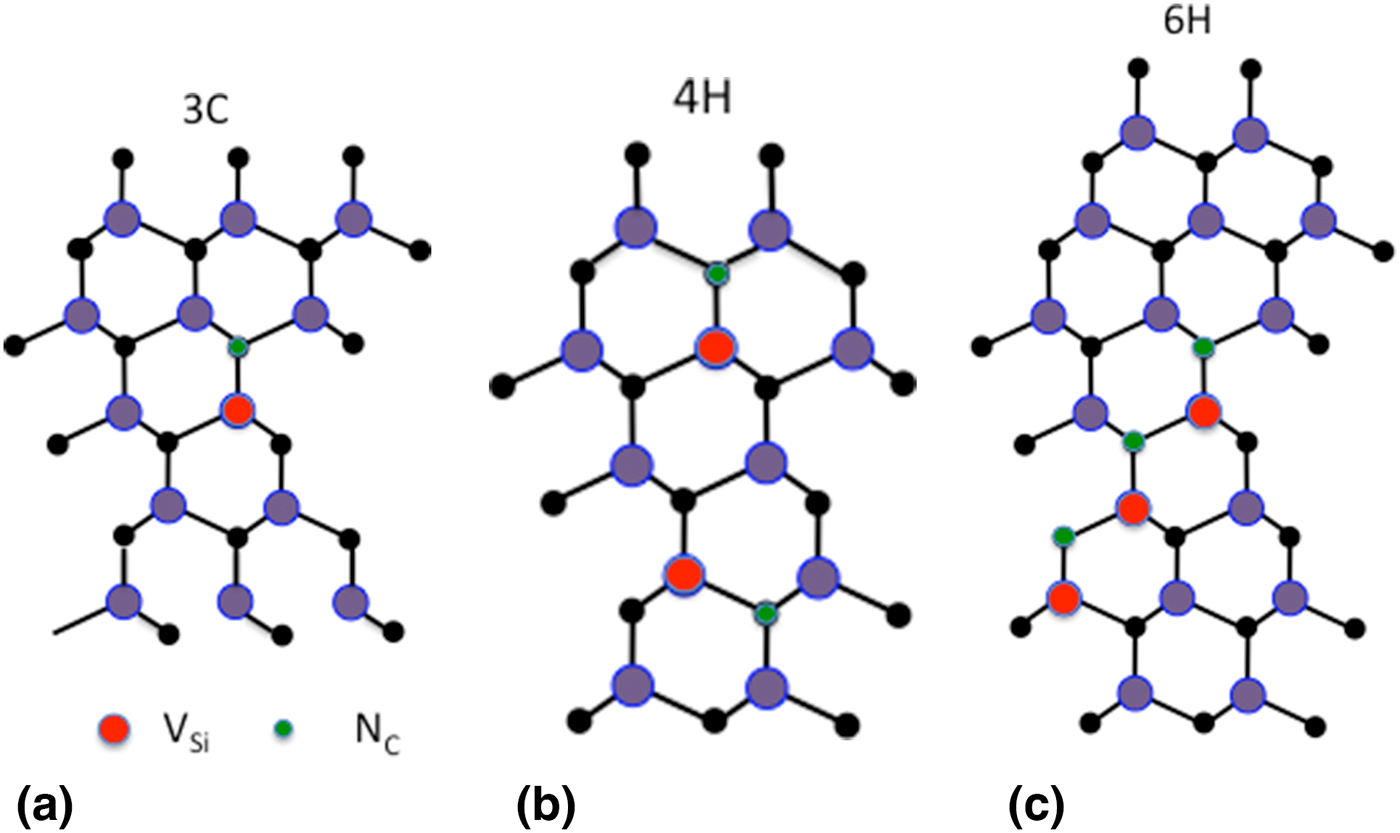
Figure 1. (a) Microscopic structure of the NV center in 3C-SiC (blue and black spheres represent Si and C atoms, respectively). (b) Axial and basal NV centers in 4H-SiC. (c) The three distinct axial NV centers in 6H-SiC.
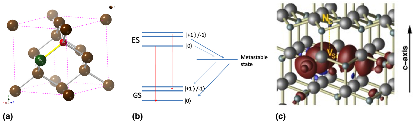
Figure 2. (a) Microscopic structure of the NV center in diamond. (b) Schematic electronic structure of the NV center in diamond and in 4H-SiC. (c) Spin density distribution of the axial NV(k) center in 4H-SiC.
As we have shown recently, all of them have a closely related electronic structure [Fig. 2(b)], which in the 1-chargestate has a spin S = 1 groundstate and a spin S = 1 excited state. In the groundstate, the spin density distribution is highly localized on the three carbon nearest-neighbor atoms and has only a weak interaction with the nitrogen atom [Fig. 2(c)]. As the VSi–NC center in SiC has different charge transition levels 0/+, 1−/0, 2−/1− and it is the 1− charge state, which has the required high-spin properties, Fermilevel engineering is required to assure that all NV centers are in the 1-charge state. Whereas this is already obtained in the smaller bandgap 3C polytype in nitrogen-doped n-type samples, an electrical compensation of n-type 4H and 6H samples is necessary to lower the Fermilevel below the shallow donor level.
We have recently shown[Reference von Bardeleben, Cantin, Rauls and Gerstmann10–Reference von Bardeleben, Cantin, Csoré, Gali, Rauls and Gerstmann12] that the expected magnetic and electronic properties of NV centers in SiC are in good agreement with the experimental findings. The NV center in SiC is not a native defect. But as we have demonstrated, the controlled formation of NV centers in the three most important polytypes of SiC (3C, 4H, 6H) can be achieved by particle (electron, proton, and ion) irradiation. The formation of NV centers is a two-step process: first silicon monovacancy must be generated and in a second step high temperature (800 °C) annealing can be used to form NV centers by VSi diffusion and association with NC centers.
Characteristic common features of the NV centers in SiC are an easily resolved hyperfine interaction of the electron spin with the nuclear spin of the nitrogen neighbor and a narrow photoluminescence zero phonon line (ZPL) [Fig. 3(c)] associated with the spin-dependent recombination between the 3E–3A2 defect states.[Reference Zargaleh, Eblé, Hameau, Cantin, Legrand, Bernard, Margaillan, Lauret, Roch, von Bardeleben, Rauls, Gerstmann and Treussart11] A major difference between NV centers in diamond and SiC is the spectral range for these optical transitions, which is shifted from the red in diamond to the infrared (1.2–1.5 µm) depending on the polytype and lattice sites of VSi and NC [Fig. 3(c)]. Due to the presence of an intermediate singlet state [Fig. 2(b)] participating in the recombination process, optically induced ground state spin polarization is possible and has been observed in all three cases.

Figure 3. (a) EPR spectrum of the NV(k) center in 4H-SiC with resolved 14N hyperfine structure. (b) Temperature dependence of the zero-field splitting parameter of the NV(k) center in 4H-SiC. (c) ZPL photoluminescence spectra of the four NV centers in 4H-SiC.
A further important difference in non-isotopically modified SiC is the presence of two nuclei with non-zero spin: the 4.7 at. % 29Si (I = 1/2) and the 1 at.% Reference Christle, Klimov, de la Casas, Szasz, Ivady, Jokubavicius, ul Hassan, Syväjärvi, Koehl, Ohshima, Son, Janzén, Gali and Awschalom13C (I = 1/2). Their presence is the reason for increased spin coherence times due to dynamic nuclear decoupling. Further, electronic polarization transfer to either of them is in principle possible.
The ground state spin Hamiltonian parameters of the axial NV centers in the different polytypes are given in Table I. The experimental values have been mainly obtained from electron paramagnetic resonance (EPR) measurements. They are compared with ab initio calculated values.[Reference von Bardeleben, Cantin, Csoré, Gali, Rauls and Gerstmann12] The good agreement between theory and experimental results has allowed the assignment of the different NV centers in SiC.
Table I. Spin Hamiltonian parameters of the axial NV centers in SiC.[Reference von Bardeleben, Cantin, Csoré, Gali, Rauls and Gerstmann12]

In addition to the axial NV centers in which the defects axis is aligned parallel to the c-axis, basal NV centers are equally formed by the VSi diffusion process. We show in Fig. 4(a) the EPR spectrum of the two types (hk, kh) of basal NV centers in 4H-SiC. Their point symmetry is lowered to C1h and they are characterized by a non-zero rhombic zero-field splitting parameter E. The calculated zero field splitting (ZFS) parameters are in good agreement with the experimental values, but the D values show a systematic shift of ≈100 MHz [Fig. 4(b)], which has been attributed to the fact that the spin–orbit coupling contribution has not been considered in these calculations. The basal NV centers have also distinct ZPL photoluminescence lines [Fig. 3(c)] in the near infrared close to the ZPL of the axial centers.

Figure 4. (a) EPR spectrum of the axial and basal NV centers in 4H-SiC for B//c. (b) Experimental (circle) and calculated (square) ZFS parameters (D, E) for the basal NV centers in 4H-SiC.
The spin density distribution of the groundstate is strongly localized on the three carbon atoms, which are next to the silicon vacancy and to a less extend on the next-nearest Si and C neighbors. It has only a weak localization on the nitrogen atom with a hyperfine coupling constant of typically 1 MHz; but due to the small linewidth (200 mG) of the EPR lines in SiC, the hyperfine interaction is nevertheless resolved in the EPR spectra [Fig. 3(a)]. This characteristic feature allows a simple distinction between NV centers and divacancy centers (VSiVC)°, which have similar zero-field splitting parameters. As in the case of diamond, the zero-field splitting parameter D of the NV centers in SiC shows temperature dependence [Fig. 3(b)], which allows their application as a nanoscale temperature sensor.
The spin coherence times of NV centers are expected to be long: first results in 4H-SiC show values of T 2 = 30 µs at T = 90 K [Figs. 5(a) and 5(b)]. Much longer times in highly diluted samples can be expected at low temperature. Single defect spectroscopy and single photon emission has not yet been shown for NV centers in 4H-SiC, but have been demonstrated for the closely related VSi–VC centers[Reference Christle, Klimov, de la Casas, Szasz, Ivady, Jokubavicius, ul Hassan, Syväjärvi, Koehl, Ohshima, Son, Janzén, Gali and Awschalom13]; similar achievements can be expected for NV centers shortly. Then, entanglement of spin–spin and spin–photons[Reference Economou and Dev14] will become accessible with the NV centers. The superior material properties of SiC, which can be obtained as n-type conductive, p-type or semi-insulating epitaxial layers as well as its demonstrated nanostructuring should allow finally to integrate all functionalities on a single SiC chip.
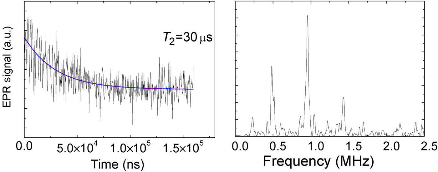
Figure 5. (a) T 2 measurement of the ms = /0−>1 transition of the NV(k) center in 4H-SiC; T = 90 K. (b) ESEEM spectrum displaying the nuclear hyperfine interactions.


