Introduction
III-N-V materials, such as GaNP and GaNAs, have a very large band-gap bowing and are very promising for light-emitting devices with a very wide wavelength region from ultraviolet to infrared [Reference Bellaiche, Wei and Zunger1,Reference Wei and Zunger2]. They are expected to realize a wider range of bandgaps with a smaller lattice mismatch to GaN.
However, III-N-V type alloys can be hardly grown under an equilibrium condition, since they have a very large miscibility gap [Reference Stringfellow3,Reference Stringfellow4]. The gas-source molecular-beam epitaxy (GSMBE) growth of nitrogen (N) rich hexagonal (h) GaNAs [Reference Iwata, Asahi, Asami, Kuroiwa and Gonda5] and GaNP [Reference Iwata, Asahi, Asami and Gonda6,Reference Tampo, Asahi, Iwata, Hiroki, Asami and Gonda7] alloys on sapphire substrates and their optical properties have been recently reported. The maximum As and P concentrations of these alloys with a hexagonal structure are so far limited to 0.26% [Reference Iwata, Asahi, Asami and Gonda6] and 8.3% [Reference Tampo, Asahi, Iwata, Hiroki, Asami and Gonda7], respectively. However, there has been no report on a metalorganic chemical vapor deposition (MOCVD) growth of cubic-GaNAs using the dimethylhydrazine (DMHy). In this paper, the As effect for hexagonal growthsuppression on cubic GaNAs growth is reported in MOCVD.
Experimental
GaNAs was grown on a GaAs (001) substrate using a horizontal MOCVD apparatus. The pressure in the reactor was 160 Torr. Trimethylgallium (TMG), DMHy [(CH3)2NNH2] and arsine (AsH3) were used as precursors of Ga, N, and As, respectively. A GaN buffer layer of about 20 nm in thickness was grown on the substrate using TMG and DMHy at 853 K. After that, a GaNAs layer was grown on the GaN buffer layer at 1193 K under the conditions of different AsH3 flows. The growth temperature was constant at 1193 K, since when the growth temperatures were lower than 1193 K and also higher than 1223 K, the grown surface became rough. The surface morphologies of the samples were observed by scanning electron microscopy (SEM), and the surface roughness was measured by atomic force microscopy (AFM). The crystal structure was investigated by an X-ray diffraction (XRD) measurement. Secondary ion mass spectrometry (SIMS) was carried out to estimate As incorporation into the c-GaN films. To investigate the optical properties, a photoluminescence measurement of GaNAs was carried out using a He-Cd laser (325 nm) at 5K.
Results and Discussion
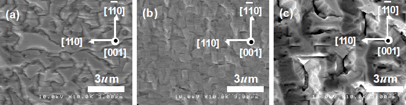
In order to increase the As incorporation into cubic GaNAs, the AsH3 flow rate was changed from 0 to 450 μmol/min and the flow rates of TMG and DMHy were fixed at 18 and 230 µmol/min, respectively. Without AsH3 flow, the growth rate of c-GaN was 1.5 nm/sec. When the AsH3 flow was increased to 450 μmol/min, the growth rate was reduced to 1.0 nm/sec. The thickness of the epitaxial layers was approximately 600 nm. Figure 1 shows the surface morphologies of the samples at different AsH3 flow rates ranging from 0 to 450 μmol/min, observed by SEM. Figure 1 (a) shows GaN surface morphologies without AsH3 flow. The shape of the grains is elongated in the [110] direction and the length of each grain is several microns. These grains have a tendency to form (111) B facets and (113) A facets [Reference Wu, Kudo, Nagayama, Yaguchi, Onabe and Shiraki8]. Figure 1 (b) shows the surface morphologies in the case of AsH3 flow under 225 μmol/min. The surface was smooth and the grains were smaller with more isotropic shapes. When the AsH3 flow rate was, moreover, as large as 450 μmol/min, the GaNAs growth was more three dimensional and the grains were also isotropic and larger.

Figure 1. SEM images of samples with various AsH3 flow rates ranging from 0 to 450 μ mol/min.(a) AsH3=0 μ mol/min, ¶=AsH3/(AsH3+DMHy)=0,(b) AsH3=225 μ mol/min, ¶=0.49, (c) AsH3=450 μmol/min, ¶=0.66.
We also observed the AFM images in order to investigate the surface roughness of GaNAs layers grown at different AsH3 flow rates (0 ∼ 225 μmol/min). It was found that the surface became smoother with increasing the AsH3 flow rate. That is, the root-mean-square (rms) showing a surface roughness became smaller than 22.7 nm with increasing the AsH3 flow rate. The above-mentioned results of SEM and AFM indicate that with AsH3 the grain size and shape was smaller and more isotropic, and that the surface was smoother, although the growth rate decreased wth increasing AsH3 flow. This is considered to be due to As adsorption on the GaN surface during the growth process. It is considered that As adsorption on the GaN surface lowers the surface energy to stabilize the (001) surface, resulting in suppressing the generation of a hexagonal structure, as Foxon et al previously reported [Reference Cheng, Jenkins, Hooper, Foxon, Orton and Lacklison9].
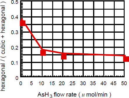
Figure 2 shows three-dimensional maps of XRD of the two grown layers with and without AsH3 flow. The X-ray incident azimuth was the {1-10} direction. Two different diffraction peaks from h-GaN (1-101) were observed along with the main diffraction from c-GaN (002), as shown in Figure 2 (a). With this X-ray incident azimuth, the h-GaN (1-101) domains, holding on two different (111) B surfaces, were observed. The diffraction-peak intensity from h-GaN (1-101) on (111) B surfaces was much larger than from h-GaN on (111) A surfaces; this is consistent with that the grains at the c-GaN surface have (111) B facts and do not have (111) A facets. Interestingly, with AsH3 flow, the diffraction intensity from h-GaN (1-101) becomes significantly weaker. This tendency was common to these samples with AsH3 flow under 225 μmol/min. We estimated the concentration of the hexagonal phase in the c-GaN layers by comparing with the integrated diffraction intensities of c-GaN (002) and h-GaN (1-101) [Reference Tsutchiya, Sunaba, Yonemura, Suemasu and Hasegawa10]. It is considered that with AsH3 flow during the c-GaN growth, As adsorbs on the GaN (001) surface and prevents the generation of (111) facets, resulting in maintaining the surface flatness. This smooth surface is favorable to c-GaN growth, because h-GaN is easy to grow with its c-axis parallel to the <111> directions. Figure 3 shows the concentration of the hexagonal phase in epilayers at different AsH3 flow rates. It was confirmed that with increasing the AsH3 flow the concentration of the hexagonal phase significantly decreased to 15%. That is, this growth condition is very effective for suppressing of hexagonal GaNAs.

Figure 2. Three-dimensional graphs of reciprocal space maps of (a) c-GaN and (b) c-GaNAs (AsH3 flow rate was 90 μmol/min) with X-ray beams incident along the <1010> azimuth.

Figure 3. Concentration of the hexagonal phase in the c-GaN layers with various AsH3 flow rates.
Figure 4 shows SIMS depth profiles of the samples with AsH3 flow of 0 and 225 μmol/min. The As intensity of the samples with an AsH3 flow rate of 225 μmol/min became larger, as large as 20 in the same scale. The As counts increased according to the increase in the AsH3 flow rate up to 225 μmol/min. Therefore, As was actually incorporated in the c-GaN layers by the AsH3 flow. When the AsH3 flow rate was 450 μmol/min, GaNAs polycrystals were observed in the GaNAs layer. In order to further incorporate the As into GaNAs, the growth condition must to be further improved.

Figure 4. SIMS depth profiles of (a) c-GaN (without AsH3 flow), (b) c-GaNAs (AsH3 flow rate was 225 μmol/min).
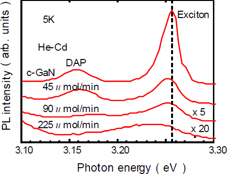
We next carried out a photoluminescence (PL) measurement of GaNAs grown at different AsH3 flow rates to investigate the optical properties. The two main peaks were observed. That is, the excitonic emission at 3.256 eV and the donor-acceptor pair recombination at 3.156 eV were observed in the PL spectrum of c-GaN. With increasing the AsH3 flow rate, the excitonic emission became weak and the deep luminescence band around 2.8 eV became dominant. Figure 5 shows the near-band-edge emission of the GaNAs PL spectra. With increasing the AsH3 flow rate, the exciton peak shifts toward lower energies and becomes broad. This is due to As incorporation in the c-GaN layer. The maximum value of the peak shift is 20 meV, which corresponds to approximately 0.1% As concentration, as estimated from the bowing parameter of h-GaNAs (19.6 eV) [Reference Iwata, Asahi, Asami, Kuroiwa and Gonda5].

Figure 5. PL spectra of near-band edges with various AsH3 flow rates at 5k.
Conclusion
The hexagonal domain suppression-effects in c-GaNAs grown by MOCVD using DMHy were investigated. GaNAs samples were grown at different AsH3 flow rates (0 ∼ 450 μmol/min) at 1193 K. As a result, three types of surface morphologies were obtained: the first was obtained as a smooth surface (AsH3 = 0 µmol/min); the second was a smooth surface having small and isotropic grains (AsH3 : 45 ∼ 225 μmol/min ); and the third involved three-dimensional surface morphologies (above 450 μmol/min of AsH3 flow rate). Furthermore, it was confirmed using X-ray diffraction that the mixing ratio of hexagonal GaNAs in cubic GaNAs decreased along with an increase in the AsH3 flow rate. We could obtained a GaNAs having a cubic component above 85% at AsH3 flow rates above 20 μmol/min. Therefore, the MOCVD growth method using AsH3 and DMHy was effective for suppressing hexagonal GaNAs.
Acknowledgements
This work was supported by NEDO/JRCM’s "The Light for the 21’ Century" Japanese national project.