Hostname: page-component-848d4c4894-m9kch Total loading time: 0 Render date: 2024-05-07T14:58:13.027Z Has data issue: false hasContentIssue false

Fast smoothing on diamond surface by inductively coupled plasma reactive ion etching

Published online by Cambridge University Press:  09 December 2019

Yuting Zheng
Affiliation:
Institute for Advanced Materials and Technology, University of Science and Technology Beijing, Beijing 100083, People’s Republic of China School of Engineering, University of Leicester, Leicester LE1 7RH, U.K.
Jinlong Liu
Affiliation:
Institute for Advanced Materials and Technology, University of Science and Technology Beijing, Beijing 100083, People’s Republic of China
Ruoying Zhang
Affiliation:
School of Engineering, University of Leicester, Leicester LE1 7RH, U.K.
Aude Cumont
Affiliation:
School of Engineering, University of Leicester, Leicester LE1 7RH, U.K.
Jue Wang
Affiliation:
School of Materials Science and Engineering, University of Science and Technology Beijing, Beijing 100083, People’s Republic of China
Junjun Wei
Affiliation:
Institute for Advanced Materials and Technology, University of Science and Technology Beijing, Beijing 100083, People’s Republic of China
Chengming Li*
Affiliation:
Institute for Advanced Materials and Technology, University of Science and Technology Beijing, Beijing 100083, People’s Republic of China
Haitao Ye*
Affiliation:
School of Engineering, University of Leicester, Leicester LE1 7RH, U.K.
*
a)Address all correspondence to these authors. e-mail: chengmli@mater.ustb.edu.cn
Get access

Abstract

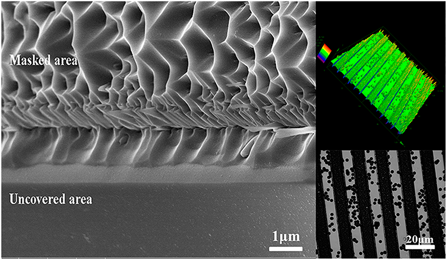
The synergetic effects of surface smoothing exhibited during the inductively coupled plasma reactive ion etching (ICP-RIE) of free-standing polycrystalline diamonds (PCDs) were investigated. Changing the assistive gas types generated variable surface oxidation states and chemical environments that resulted in different etching rates and surface morphologies. The main reaction bond mechanism (C–O) during ICP-RIE and the ratio of C–O–C/O–C=O associated with the existence of a uniform smooth surface with root mean square (RMS) roughness of 2.36 nm were observed. An optimal process for PCD smoothing at high etching rate (4.6 μm/min) was achieved as follows: 10% gas additions of CHF3 in O2 plasma at radio frequency power of 400 W. The further etched ultra-smooth surface with RMS roughness <0.5 nm at etching rate of 0.23 μm/min that being produced by transferring this optimum recipe on single crystal diamonds with surface patterns confirmed the effectiveness of the fast smoothing approach and its feasibility for diamond surface patterning.

Type
Article
Copyright
Copyright © Materials Research Society 2019

Access options

Get access to the full version of this content by using one of the access options below. (Log in options will check for institutional or personal access. Content may require purchase if you do not have access.)

References

Maze, J.R., Stanwix, P.L., Hodges, J.S., Hong, S., Taylor, J.M., Cappellaro, P., Jiang, L., Dutt, M.V.G., Togan, E., Zibrov, A.S., Yacoby, A., Walsworth, R.L., and Lukin, M.D.: Nanoscale magnetic sensing with an individual electronic spin in diamond. Nature 455, 644647 (2008).CrossRefGoogle Scholar
Zheng, Y.T., Liu, J.L., Wang, J.J., Li, Z.C., Hao, H., Wei, J.J., Chen, L.X., Ye, H.T., and Li, C.M.: The direct-current characteristics and surface repairing of a hydrogen-terminated free-standing polycrystalline diamond in aqueous solutions. J. Phys. Chem. Solids 130, 111119 (2019).CrossRefGoogle Scholar
Ekimov, E.A., Sidorov, V.A., Bauer, E.D., Me’nik, N.N., Curro, N.J., Thompson, J.D., and Stishov, S.M.: Superconductivity in diamond. Nature 428, 542545 (2002).CrossRefGoogle Scholar
Yuan, X.L., Zheng, Y.T., Zhu, X.H., Liu, J.L., Liu, J.W., Li, C.M., Jin, P., and Wang, Z.G.: Recent progress in diamond based MOSFETs. Int. J. Miner., Metall. Mater. 26, 11951205 (2019).CrossRefGoogle Scholar
Sussmann, R.S., ed.: CVD Diamond for Electronic Devices and Sensors (John Wiley & Sons, Chichester, 2009).CrossRefGoogle Scholar
Nojiri, K., ed.: Dry Etching Technology for Semiconductors (Springer, Switzerland, 2012).Google Scholar
Tao, Y. and Degen, C.L.: Single-crystal diamond nanowire tips for ultrasensitive force microscopy. Nano Lett. 15, 78937897 (2015).CrossRefGoogle ScholarPubMed
Toros, A., Kiss, M., Graziosi, T., Sattari, H., Gallo, P., and Quack, N.: Precision micro-mechanical components in single crystal diamond by deep reactive ion etching. Microsyst. Nanoeng. 4, 12 (2018).CrossRefGoogle ScholarPubMed
Achard, J., Tallaire, A., Mille, V., Naamoun, M., Brinza, O., Boussadi, A., William, L., and Gicquel, A.: Improvement of dislocation density in thick CVD single crystal diamond films by coupling H2/O2 plasma etching and chemo mechanical or ICP treatment of HPHT substrates. Phys. Status Solidi A 212, 22642267 (2014).CrossRefGoogle Scholar
Hiscocks, M.P., Kaalund, C.J., Ladouceur, F., François, L., Huntington, S.T., Gibson, B.C., Trpkovski, S., Simpson, D., Eric, L.A., Steven, P., and James, B.E.: Reactive ion etching of waveguide structures in diamond. Diamond Relat. Mater. 17, 18311834 (2008).CrossRefGoogle Scholar
Izak, T., Kromka, A., Babchenko, O., Ledinsky, M., Hruska, K., and Verveniotis, E.: Comparative study on dry etching of polycrystalline diamond thin films. Vacuum 86, 799802 (2012).CrossRefGoogle Scholar
Kunuku, S., Sankaran, K.J., Tsai, C., Chang, W., Tai, N., Leou, K., and Lin, I.N.: Investigations on diamond nanostructuring of different morphologies by the reactive-ion etching process and their potential applications. ACS Appl. Mater. Interfaces 5, 74397449 (2013).CrossRefGoogle ScholarPubMed
Leech, P., Reeves, G., and Holland, A.: Reactive ion etching of diamond in CF4, O2, O2, and Ar-based mixtures. J. Mater. Sci. 14, 34533459 (2001).CrossRefGoogle Scholar
Shiomi, H.: Reactive ion etching of diamond in O2 and CF4 plasma, and fabrication of porous diamond for field emitter cathodes. Jpn. J. Appl. Phys. 36, 7745 (1997).CrossRefGoogle Scholar
Dorsch, O., Werner, M., and Obermeier, E.: Dry etching of undoped and boron doped polycrystalline diamond films. Diamond Relat. Mater. 4, 456459 (1995).CrossRefGoogle Scholar
Ando, Y., Nishibayashi, Y., Kobashi, K., Hirao, T., and Oura, K.: Smooth and high-rate reactive ion etching of diamond. Diamond Relat. Mater. 11, 824827 (2002).CrossRefGoogle Scholar
Schmitt, J., Nelissen, W., Wallrabe, U., and Völklein, F.: Implementation of smooth nanocrystalline diamond microstructures by combining reactive ion etching and ion beam etching. Diamond Relat. Mater. 79, 164172 (2017).CrossRefGoogle Scholar
Lee, C.L., Gu, E., Dawson, M.D., Friel, I., and Scarsbrook, G.A.: Etching and micro-optics fabrication in diamond using chlorine-based inductively coupled plasma. Diamond Relat. Mater. 17, 12921296 (2008).CrossRefGoogle Scholar
Yamada, T., Yoshikawa, H., Uetsuka, H., Somu, K., Norio, T., and Ichi, S.S.: Cycle of two-step etching process using ICP for diamond MEMS applications. Diamond Relat. Mater. 16, 996999 (2007).CrossRefGoogle Scholar
Forsberg, P. and Karlsson, M.: High aspect ratio optical gratings in diamond. Diamond Relat. Mater. 34, 1924 (2013).CrossRefGoogle Scholar
Muchnikov, A.B., Vikharev, A.L., Butler, J.E., Chernov, V.V., Isaev, V.A., Bogdanov, S.A., Okhapkin, A.I., Yunin, P.A., and Drozdov, Y.N.: Homoepitaxial growth of CVD diamond after ICP pretreatment. Phys. Status Solidi 212, 25722577 (2015).CrossRefGoogle Scholar
Uetsuka, H., Yamada, T., and Shikata, S.: ICP etching of polycrystalline diamonds: Fabrication of diamond nano-tips for AFM cantilevers. Diamond Relat. Mater. 17, 728731 (2008).CrossRefGoogle Scholar
Cui, Z., ed.: Micro-Nanofabrication Technologies and Applications (Higher Education Press, China, 2009).Google Scholar
Castelletto, S., Rosa, L., Blackledge, J., Zaher, M., Abri, A., and Boretti, A.: Advances in diamond nanofabrication for ultrasensitive devices. Microsyst. Nanoeng. 3, 17061 (2017).CrossRefGoogle ScholarPubMed
Jackson, M.J. and Ahmed, W., eds.: Micro and Nano-Manufacturing, Vol. II (Springer, New York, 2018).Google Scholar
Zheng, Y.T., Ye, H.T., Liu, J.L., Wei, J.J., Chen, L.X., and Li, C.M.: Surface morphology evolution for polycrystalline diamond by inductively coupled plasma reactive ion etching (ICP-RIE). Mater. Lett. 253, 276280 (2019).CrossRefGoogle Scholar
Iqbal, S., Rafique, M.S., Akhtar, S., Liaqat, N., Iqbal, N., and Ahma, R.: A comparative study on finding an effective root for the introduction of hydrogen into micro plasma during diamond growth. J. Phys. Chem. Solids 122, 7286 (2018).CrossRefGoogle Scholar
Dychalska, A., Fabisiak, K., Paprocki, K., Jarosław, M., Aizhan, I., and Mirosław, S.: A Raman spectroscopy study of the effect of thermal treatment on structural and photoluminescence properties of CVD diamond films. Mater. Des. 15, 320327 (2016).CrossRefGoogle Scholar
Crist, B.V.: XPS in industry—Problems with binding energies in journals and binding energy databases. J. Electron Spectrosc. Relat. Phenom. 231, 7587 (2019).CrossRefGoogle Scholar
Varga, M., Izak, T., Vretenar, V., Kozak, H., Holovsky, J., Artemenko, A., Hulman, M., Skakalova, V., Lee, D.S., and Kromka, A.: Diamond/carbon nanotube composites: Raman, FTIR and XPS spectroscopic studies. Carbon 111, 5461 (2017).CrossRefGoogle Scholar
Pan, X.Y., Wang, L.J., Zeng, Q.K., Shi, L.Y., Xu, R., Huang, J., Tang, K., and Xia, Y.B.: XPS study of polycrystalline diamond surfaces after annealing treatment. Surf. Coat. Technol. 228, S446S448 (2013).CrossRefGoogle Scholar
Birrell, J., Gerbi, J., Auciello, O., Gibson, J., Gruen, D., and Carlisle, J.: Bonding structure in nitrogen doped ultrananocrystalline diamond. J. Appl. Phys. 93, 56065612 (2003).CrossRefGoogle Scholar
Hassan, M.M. and Larsson, K.: Effect of surface termination on diamond (100) surface electrochemistry. J. Phys. Chem. C 118, 2299523002 (2014).CrossRefGoogle Scholar
Tressaud, A., Moguet, F., Flandrois, S., Chambon, M., Guimon, C., Nanse, G., Papirer, E., Gupta, V., and Bahl, O.P.: On the nature of C–F bonds in various fluorinated carbon materials: XPS and TEM investigations. J. Phys. Chem. Solids 57, 745751 (1996).CrossRefGoogle Scholar
Dunitz, J.D. and Taylor, R.: Organic fluorine hardly ever accepts hydrogen bonds. Chem. - Eur. J. 3, 8998 (1997).CrossRefGoogle Scholar
Sun, B., Zhang, X., Zhang, Q., and Lin, Z.: Effect of atomic hydrogen and oxygen on diamond growth. J. Appl. Phys. 73, 46144617 (1993).CrossRefGoogle Scholar