Introduction
Recently, there has been much progress in the research and development of AlGaN/GaN High Electron Mobility Transistors (HEMTs). However, the physics of these novel devices has not yet been fully understood. In this paper, we report on a new mechanism of the negative differential mobility in AlGaN/GaN HEMTs.
Negative differential conductance (NDC) in HEMTs was previously observed [Reference Shur, Arch, Daniels and Abrokwah2-Reference Gaska, Osinsky, Yang and Shur3]. However, in these publications, the NDC was attributed to either gate leakage current [Reference Shur, Arch, Daniels and Abrokwah2] or self-heating effect [Reference Gaska, Osinsky, Yang and Shur3]. In [Reference Shur, Arch, Daniels and Abrokwah2], it was claimed that the two dimensional electron gas was heated in the channel. This heating caused the “real-space transfer” [Reference Hess, Markoc, Shichijo and Streetman4] between the GaAs conducting layer and the AlGaAs barrier layer. Self-heating might also lead to NDC [Reference Gaska, Osinsky, Yang and Shur3] since with the maximum sourcedrain current of 1A/mm, the GaN devices grown on sapphire biased at 5V could have a temperature rise of 125K, which would significantly reduce the mobility and the maximum charge density of the channel.
In our samples, these mechanisms do not play an important role for the following reasons. Self-heating is not important since the power dissipation in our samples is only on the order of 0.5W/mm. For an estimated impedance of 25W/mm [Reference Gaska, Osinsky, Yang and Shur3], this power dissipation should lead to the temperature rise of 12K, which is not enough to cause NDC.
As shown below, piezoelectric and pyroelectric effects in AlGaN/GaN heterostructures hinder the real space transfer into the AlGaN layer. However, as we discuss below, real space transfer into the 3D states in GaN is a possible mechanism explaining the observed NDC.
Experiments
The Al0.2Ga0.8N/GaN HEMTs were grown on sapphire substrates by low-pressure metal organic chemical vapor deposition (MOCVD). The epilayer design of the samples was described in [Reference Gaska, Chen, Asif Khan, Ping, Adesida and Shur5]. The measured 2DEG sheet density was on the order of 1012cm−2 and the Hall mobility was 1,000 cm2/V.s.
Figure 1(a) shows the current-voltage characteristics of the 45 μm wide AlGaN-GaN HEMT. The source-drain spacing Lds was 5 μm and the gate length Lg was 1.7μm. The applied gate bias was as high as 3.0 V. The negative differential conductivity (NDC) was observed at the gate biases Vg > 1.5 V. The drain current increased with Vds to the peak value, Ipeak, determined by the gate bias, and then decreased until saturation current (Isat) has been reached. For HEMTs with the drainto-gate spacing of 1 μm and 2 μm the peak drain current was achieved at the source-drain voltages of approximately Vpeak = 1.5 V and Vpeak = 2.5 V, respectively. The NDC was observed at the source-drain voltages Vpeak < Vds < Vvalley, where Vvalley was the drain bias when the NDC effect stopped. The drain current reached its saturation beyond Vvalley. In Figure 1(b), we show the gate bias dependence of Vpeak, Vvalley and the peak-valley current ration R=Ipeak/Ivalley. This figure demonstrates that Vvalley increased with the gate bias with a slope of about 1, while the increase rate of Vpeak was much smaller. On the other hand, R also increased almost linearly with Vg.

Figure 1. Drain current-voltage characteristics of the 45 μm wide AlGaN-GaN HEMT. (a) Drain current dependence on Vd, Vg varies from 0 to 3V with the step of 0.5V. (b) The Vpeak, Vvalley and Ipeak/Isat as functions of the gate bias.
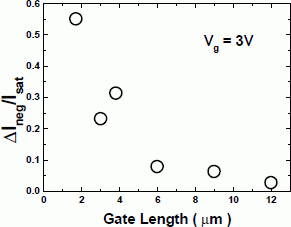
We measured NDC in the HEMTs with the source-drain spacing from 5μm to 15μm and the offset gate length from 2μm to 12μm. The source-to-gate and gate-to-drain distances were approximately the same and equal to 2μm and 1μm, respectively. Figure 2 demonstrates the normalized current drop as a function of the gate length for 95 μm wide HEMTs (ΔIneg = Ipeak - Isat). The obtained results clearly showed strong dependence of NDC on Lg. At the gate bias of +3.0 V, the increase in the gate length for about 6 times (source-drain spacing increases 3 times) reduces NDC by a factor of larger than 30. The saturation current for the same gate lengths decreases linearly only by one third, from 12 mA to 8 mA. The ΔIneg dependence on the gate length can be described by expression ΔIneg ∼ Lg −α, where α is from 1.5 to 2.

Figure 2. Gate length dependence of the current drop in NDC (normalized to the Isat)
Discussion
The gate current versus drain voltage at different gate biases for the device in Figure 1 was measured. (See also [Reference Deng, Gaska, Shur, Khan and Yang6]). Even for the zero source-drain voltage, the gate leakage current at high positive gate bias (Vg = +3.0 V) was less than 0.5 mA, whereas the drain current reduction in the NDC region for the same gate bias was more than 3mA (see Figure 1(a)). At the source-drain voltage of 1.5 V and higher (NDC region) the gate current dropped below 1μA. These results indicated that the gate current of the device were negligible compared to ΔIneg.
As we mentioned before, the device had a maximum drain current on the order of 0.1∼0.2A/mm, which would only raise the temperature by 10∼20K at a thermal impedance of 25 K·mm/W [Reference Gaska, Osinsky, Yang and Shur3]. Also, the self-heating NDC led to a monotonous decrease of the drain current in the saturation regime, whereas the NDC reported here took place in a limited drain voltage range (see Figure 1(a)). Therefore ,we concluded that both the gate current and self-heating were not the mechanism leading to the NDC in our samples.
The explanation we provided for the NDC was the mobility and sheet carrier density decrease due to the real space transfer from the 2D to 3D GaN states. First, we compared the mobility of the two-dimensional and the three-dimensional electron gas. The results are shown in Figure 3. Even at room temperature, the mobility of 2D-electron gas is around 50% larger than the mobility of 3D electrons. This difference is much larger at cryogenic temperatures.

Figure 3. Calculated 2D and 3D electron mobility in GaN at different temperatures
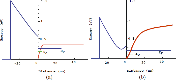
In Figure 4, we compared the band diagram of HEMTs in different material systems – GaN-based and GaAs-based. Due to the piezoelectric and pyroelectric effects, the conduction band profile in the AlGaN layer does not have a minimum that is needed for the real space transfer from GaN into AlGaN. Also, in contrast to AlGaAs/GaAs system, the energy difference between the Fermi level in the 2D gas and the bottom of the conduction band in the GaN is relatively small due to the residual doping in GaN. This small difference made the electron transition into the GaN bulk more important.

Figure 4. Comparison between the band diagram of GaN based HEMTs and GaAs based HEMTs. (a) Calculated band diagram of GaN HEMTs at the doping level of 1017cm−3 (b) Qualitative band diagram of GaAs HEMTs
Hence, we believe that this transfer of 2D electrons into 3D GaN states reduces the channel mobility and the 2D-electron sheet concentration and leads to the current drop in the NDC region. The Monte-Carlo simulation results for AlGaAs/GaAs HEMTs reported in [Reference Widiger, Hess and Coleman7] also pointed out to the possibility of such a mechanism (see Figure 5). The dash-dotted line in Figure 5 shows the electron concentration in the quantum well and the full lines show the bulk GaAs electron concentration. This figure demonstrates that the electrons inside the quantum well experience the transition into the GaAs buffer along the channel. However, due to the low barrier height of the GaAs transistors (Figure 4(b)), the gate current becomes dominant at higher gate biases, which makes it difficult to observe the NDC related to such a transfer in GaAs devices at room temperature.

Figure 5. Monte Carlo simulation results on electron concentration in GaAs based HEMTs. Dashed dotted line, concentrations in a quantum well; full line, concentrations in bulk GaAs. After [Reference Widiger, Hess and Coleman7]
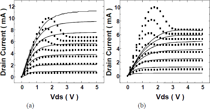
In order to illustrate this new mechanism of NDC, we calculated the current-voltage characteristics of our devices for different values of the electron mobility using the AIM-Spice [Reference Fjeldly, Ytterdal and Shur8], which helped to understand the device operation. In Figure 6(a), a mobility of 750 cm2/V.s was used and reasonable agreement was reached in the low drain bias region. The mobility dropped to 400 cm2/V.s in Figure 6(b), which give reasonable fit in the saturation region. The maximum sheet charge density for these two regions was also different. (See Table 1) These simulation results confirm that a mobility drop at the higher gate bias might be the cause of the NDC effect, as illustrated in Figure 3.

Figure 6. AIM-Spice model of the above device. The model parameters are in Table 1. The symbols are the experimental results and the lines are from simulation.
Table 1. AIM-Spice parameters for Figure 6.

Conclusions
In this paper, we report the non-thermal negative differential conductance in AlGaN/GaN HEMTs. With the help of device characterization and modeling, we excluded the possibility of selfheating and real space transfer into the AlGaN layer current as the causes of the NDC. We linked the NDC to the mobility reduction caused by the transfer from 2D to 3D states in the channel. This mechanism was supported by the device simulation and band diagram calculations.
Acknowledgements
The work has been supported by the Office of Naval Research (Project Monitor Dr. Colin Wood and Dr. John Zolper). We are also grateful to Dr. Knap and Dr. Roumiantsev for their useful discussions.