


Introduction
The ability to capture the dynamics of nanoscale objects in a liquid is critical for improving our understanding of a broad range of biological and chemical processes. This need has spurred the development of different reaction cells that integrate a fluid environment within various standard imaging platforms, such as fluorescence microscopy (Dukes et al., Reference Dukes, Peckys and de Jonge2010; Peddie et al., Reference Peddie, Blight, Wilson, Melia, Marrison, Carzaniga, Domart, O׳Toole, Larijani and Collinson2014) and scanning probe microscopy (Hörber & Miles, Reference Hörber and Miles2003). Among the different techniques currently available for studying processes in liquid, liquid cell electron microscopy (LC-EM) occupies a unique niche since it allows for the direct (in situ) imaging of nanoparticles (NPs) and their dynamics without the need for labeling at relatively high frame rates up to a few hundred frames per second with state-of-the-art electron detectors (Liao et al., Reference Liao, Zherebetskyy, Xin, Czarnik, Ercius, Elmlund, Pan, Wang and Zheng2014; Park et al., Reference Park, Elmlund, Ericus, Yuk, Limmer, Chen, Kim, Han, Weitz, Zettl and Alivisatos2015; Chee et al., Reference Chee, Baraissov, Loh, Matsudaira and Mirsaidov2016, Reference Chee, Anand, Bisht, Tan and Mirsaidov2019; Lin et al., Reference Lin, Chee, Raj, Král and Mirsaidov2016).
To allow volatile liquids into the vacuum environment of an EM, the liquid has to be encapsulated between thin impermeable membranes in cells that are subsequently hermetically sealed. The most widespread implementation of this concept involves microfluidic cells with silicon nitride membrane windows that are made using standard semiconductor microfabrication methods (Williamson et al., Reference Williamson, Tromp, Vereecken, Hull and Ross2003; de Jonge et al., Reference De Jonge, Peckys, Kremers and Piston2009; Zheng et al., Reference Zheng, Claridge, Minor, Alivisatos and Dahmen2009; Grogan & Bau, Reference Grogan and Bau2010). These liquid cell (LC) systems can be further adapted to include fluid flow tubing and electrical wiring, which allows us to study the evolution of nanostructures in liquid environments under electrochemical (Williamson et al., Reference Williamson, Tromp, Vereecken, Hull and Ross2003; Radisic et al., Reference Radisic, Ross and Searson2006; White et al., Reference White, Singer, Augustyn, Hubbard, Mecklenburg, Dunn and Regan2012; Gu et al., Reference Gu, Parent, Mehdi, Unocic, McDowell, Sacci, Xu, Connell, Xu, Abellan, Chen, Zhang, Perea, Evans, Lauhon, Zhang, Liu, Browning, Cui, Arslan and Wang2013; Holtz et al., Reference Holtz, Yu, Gunceler, Gao, Sundararaman, Schwarz, Arias, Abruña and Muller2014; Unocic et al., Reference Unocic, Sun, Sacci, Adamczyk, Alsem, Dai, Dudney and More2014; Chee et al., Reference Chee, Pratt, Hattar, Duquette, Ross and Hull2015; Mehdi et al., Reference Mehdi, Qian, Nasybulin, Park, Welch, Faller, Mehta, Henderson, Xu, Wang, Evans, Liu, Zhang, Mueller and Browning2015) or thermal (Chee et al., Reference Chee, Tan, Baraissov, Bosman and Mirsaidov2017) control in a relatively routine manner. While such systems are already commonly implemented in transmission electron microscope (TEM) holders, their application in the scanning electron microscope (SEM) is still rare. LC-EM studies with an SEM have an intriguing potential for multi-modal investigations where the larger chamber size allows for the concurrent use of multiple detectors and stimuli to in situ probe a chemical reaction. Moreover, the lower resolution of the SEM is not likely to be an issue for LC-EM studies because the intrinsic resolution of LC-EM, even with the best TEMs, is generally limited to a few nanometers (de Jonge et al., Reference De Jonge, Browning, Evans, Chee, Ross and Ross2016, Reference De Jonge, Houben, Dunin-Borkowski and Ross2019) due to the beam broadening from electron scattering in the liquid layer and the need to work with low electron fluxes to minimize beam-induced artifacts (Hermannsdörfer et al., Reference Hermannsdörfer, Tinnemann, Peckys and de Jonge2016; Schneider, Reference Schneider and Ross2016).
The common approaches for capturing the objects in a liquid with SEM include cooling the stage to temperatures where water condenses (Rykaczewski et al., Reference Rykaczewski, Scott and Fedorov2011; Xiao et al., Reference Xiao, Foray and Masenelli‐Varlot2018), encapsulation with a thin membrane layer such as graphene or with sealed capsules (also known as WET-SEM; Kolmakov, Reference Kolmakov and Ross2016). However, these approaches involving condensed liquids and sealed capsules are less suitable for studying dynamic chemical and electrochemical processes because they either do not allow control over the chemical environment or lack important features required in electrochemistry such as continuous fluid flow and electrodes to apply an external bias voltage or to be used as a reference. While there are home-made LC-SEM systems that also incorporate flow (Yang et al., Reference Yang, Zhu, Yu, Thevuthasan and Cowin2013; Kolmakov, Reference Kolmakov and Ross2016; Yu et al., Reference Yu, Arey, Chatterjee and Chun2019) or allow electrochemical measurements (Jensen et al., Reference Jensen, Købler, Jensen and Mølhave2013; Jensen et al., Reference Jensen, Burrows and Mølhave2014; Kolmakov, Reference Kolmakov and Ross2016; Velasco-Velez et al., Reference Velasco-Velez, Mom, Sandoval-Diaz, Falling, Chuang, Gao, Jones, Zhu, Arrigo, Roldán Cuenya, Knop-Gericke, Lunkenbein and Schlögl2020), these systems commonly utilize a single membrane window with a relatively large liquid reservoir underneath, which affects the final resolution due to the extended interaction volume of the primary electrons. The LC geometry used in TEM holders with a pair of top and bottom silicon nitride membranes has, to the best of our knowledge, not yet been reported. We expect benefits from such a geometry for LC-SEM, especially in terms of limiting beam-induced effects.
The primary mechanism behind beam-induced artifacts in LC-EM studies is the generation of radiolytic species due to the scattering of energetic electrons by the liquid. In a geometry that has only a single membrane window at the top, the amount of liquid below the window is essentially bulk and so, all the energy of the electron beam will be deposited into the liquid. Depositing all the energy of the electron beam into the liquid is not desirable for LC-SEM because of the lower energy of the primary electrons. Lower energy electrons have larger cross-sections for inelastic scattering (Egerton et al., Reference Egerton, Li and Malac2004). Furthermore, the amount of radiolytic species created is expected to increase dramatically as the primary electrons propagate through the liquid and lose energy. By allowing these electrons to transmit through a second bottom membrane, the interaction volume of the primary electrons will be truncated, which should in turn limit the generation of radiolytic species. In addition, the top and bottom window geometry allows for the detection of both backscattered (BSE) and transmitted (TE) electrons. The BSE images should largely retain the intrinsic resolution of the microscope since BSEs only travel through the top silicon nitride membrane and not the liquid, whereas the TE images acquired with segmented annular detectors may allow for contrast optimization with different acquisition modes.
In this paper, we will present imaging results obtained from an LC-SEM platform that has integrated tubing and electrodes for electrochemical studies and utilizes the same cells that are used for LC-TEM. Image sequences of ~25 nm cubic-shaped copper oxide (Cu2O) NPs in an aqueous 0.1 M KHCO3 solution and the electrochemical growth of larger Cu2O cubes from 5 mM CuSO4 and 5 mM KCl solution were captured using both, BSE and TE detectors, to demonstrate the capabilities of this setup. Interestingly, the images formed with TEs that are collected at higher scattering angles exhibit a liquid layer thickness-dependent contrast inversion when the electrolyte is introduced via the fluid tubing. The images acquired under this inverted contrast also retain spatial resolution that is comparable to the BSE images, despite our initial expectations of significant blurring due to the liquid layer. The imaging characteristics of this system as a function of liquid layer thickness are rationalized using Monte Carlo (MC) simulations. As expected, the spatial resolution in images of objects located on the top membrane and formed using BSE does not suffer from significant effects of beam broadening due to the liquid layer thickness but is instead limited by a decreasing signal-to-noise ratio due to the electron scattering background from the liquid. The dark-field (DF) to bright-field (BF) contrast inversion in the TE images starts for scattering angles above 100 mrad when the liquid layer is 250 nm thick and extends toward higher angles as the liquid gets thicker. Above 1,500 nm liquid thickness, all the angular dark-field (ADF) images below 200 mrad are inverted to BF. Hence, the DF to BF contrast inversion provides a way to estimate the liquid layer thickness in these LCs.
Materials and Methods
The SEM studies were performed using a Thermo Fisher Apreo SEM with 30 kV acceleration voltage and a working distance of 10 mm. BSE and TE detectors with annular segments were used for in situ imaging. The ADF detector angle is 0–250 mrad. The LC-SEM setup is custom-built by Hummingbird Scientific for the Apreo and has tubing for fluid flow and wiring for electrochemical control. The setup also includes inlets for an Ag/AgCl reference electrode and a Pt counter electrode. The cell consists of two chips with 200 μm × 30 μm silicon nitride windows, where the top chip also includes patterned electrodes. Prior to LC assembly, the chips are cleaned for 30 min using an ozone cleaner to render their surfaces hydrophilic.
While the spacer thickness is fixed at 250 nm, we should mention here that the actual liquid thickness is larger than the spacer size. The liquid layer at the center of the window is thicker than the edge of the window because the pressure difference between the vacuum chamber and the inside of the LC causes the bulging of the silicon nitride windows, which can result in liquid thickness variations from 250 to 1,000 nm (Holtz et al., Reference Holtz, Yu, Gao, Abruña and Muller2013; Keskin et al., Reference Keskin, Kunnas and de Jonge2019).
The Cu2O NPs used for imaging were prepared by a wet-chemical ligand-free method based on previous work (Xiong et al., Reference Xiong, Li, Zhang, Du, Miao, Ma, Han, Zhao and Xu2015). The reagents were purchased from Sigma-Aldrich (ACS reagent) and used as is. First, an alkaline-diluted solution of CuCl2 was prepared by adding 5 mL of a CuCl2 solution (0.1 M) and 15 mL of a NaOH solution (0.2 M) to 200 mL of ultrapure H2O at room temperature. After 5 min under constant magnetic stirring, 10 mL of an L-ascorbic acid solution (0.1 M) was added to the mixture. The solution was further stirred for 1 h. Then, the solution was centrifuged and washed three times, twice with an ethanol–water mixture (1:1) and once with ethanol. The synthesized NPs generally have a cubic shape. Finally, the synthesized NPs were dispersed in ethanol and then drop-casted on the top chip that is facing the electron beam (Fig. 1).
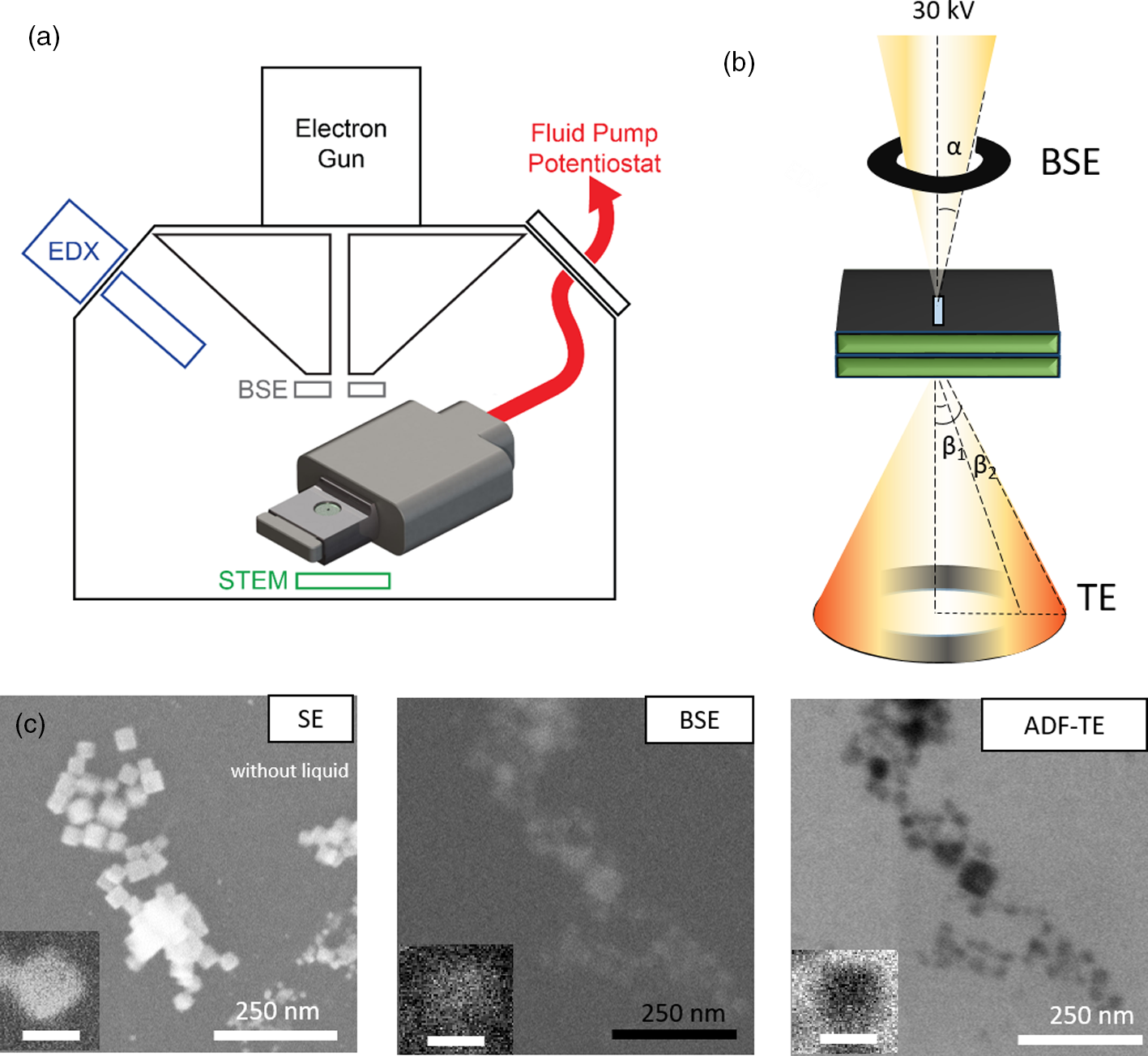
Fig. 1. (a) Schematic of the electrochemical LC-SEM setup. The SEM is equipped with BSE, STEM, and EDX detectors. The fluid and the electrical signals are delivered through tubing and wiring that are connected, respectively, to a syringe pump and a potentiostat outside of the SEM chamber. (b) The electrons scattered from the liquid cell are collected in both forward and backward directions. The forward scattered electrons are collected by the STEM detector, and the backward scattered electrons are collected by the BSE detector. The convergence angle α of the beam is 2 mrad and the collection angle β is 0–250 mrad for STEM. (c) Cu2O NPs (25 nm in size) imaged with the different electron detectors: SE, BSE, and ADF-TE from left to right. The secondary electron (SE) image shows the NPs after drop-casting on the top chip (without liquid). The BSE and ADF-TE images were acquired with 0.1 M KHCO3 electrolyte inside the assembled liquid cell. The scale bar is 25 nm in the inset.
After drop-casting, the LC was assembled and the setup leak-checked using a vacuum pump station. Then, the LC-SEM system was transferred into the SEM and the SEM was pumped down. A 25 pA probe current was used, which we found to be optimal for minimizing electron beam-induced effects (Supplementary Fig. S1). Both BSE and TE detectors were used concurrently during the image acquisition. Figures 1a and 1b show the schematics of the setup and the electrons collected from different detectors. The electrolyte is introduced into the LC inside the SEM by connecting the fluid tubing to a syringe pump outside the SEM. Figure 1c compares the images of the Cu2O NPs in 0.1 M KHCO3 solution that were acquired using the BSE and TE detectors. Supplementary Movie 1 shows that the NPs are stable under our imaging conditions and can be followed for extended periods of time without significant degradation.
For the electrochemical growth of larger Cu2O cubes, chips with a carbon electrode were used and the electrolyte consisted of 5 mM CuSO4 and 5 mM KCl. Controlled growth of cubic-shaped particles can be achieved by cycling the potential within windows of several hundred millivolts as described in our previous work (Grosse et al., Reference Grosse, Gao, Scholten, Sinev, Mistry and Roldán Cuenya2018; Arán-Ais et al., Reference Arán-Ais, Rizo, Grosse, Algara-Siller, Dembélé, Plodinec, Lunkenbein, Chee and Roldán Cuenya2020). In this case, a lower probe current of 6.3 pA was used.
MC simulations were used to model the stochastic collision events and the trajectory of electrons using the package CASINO (Demers et al., Reference Demers, Poirier‐Demers, Couture, Joly, Guilmain, de Jonge and Drouin2011). We modeled 25 × 25 × 25 nm3 Cu nanocubes enclosed by two silicon nitride membranes (50 nm each) and varied the liquid layer thickness from 0 to 1,500 nm. For simplicity, we set the liquid as pure water, assuming that the dissolved salt has a negligible effect on the electron scattering and used Cu in the model instead of Cu2O. The microscopic simulation parameters were chosen to replicate the experimental imaging conditions; the acceleration voltage is set to 30 kV, the number of simulated electrons ranged from 78,025 to 2 × 10⁵, the semi-convergence angle is 2.11 mrad, the electron probe size is 2 nm, and the ADF collection angles go from 0 to 500 mrad. We chose the Mott model (Browning et al., Reference Browning, Li, Chui, Ye and Pease1994; Drouin et al., Reference Drouin, Hovington and Gauvin1997) to calculate the total scattering cross-sectional area of each chemical element.
Experimental Results
As shown in Figure 1, the Cu2O NPs appear bright in the BSE image, whereas the liquid gives a dark background, which is expected for the mass contrast found in the BSE images. The TE image, however, does not display the expected DF image when we use the high-angle annular segments of the detector (140–250 mrad). Copper, with its larger atomic number, scatter electrons to higher angles compared to water and so, brighter contrast is expected for the NPs in the ADF images. Instead, the images show an inverted contrast that is similar to a BF image. This contrast inversion can be explained by electron scattering through the relatively thick liquid layer, where inversion in TE images in the SEM had been reported in both solid samples (Merli & Morandi, Reference Merli and Morandi2005; Morandi & Merli, Reference Morandi and Merli2007; Woehl & Keller, Reference Woehl and Keller2016) and condensed liquid layers (Xiao et al., Reference Xiao, Foray and Masenelli‐Varlot2018).
In Figure 2, BSE and TE images taken at different liquid thicknesses are presented. The liquid thickness is controlled by adjusting the pumping speed of the syringe pump. Regardless of the liquid thickness, the BSE contrast remains the same, with NPs appearing bright with a dark background. Contrary to BSE, the TE contrast undergoes the contrast inversion as the liquid thickness increases. When there is no liquid or only a thin layer of liquid, the NPs show the bright contrast expected in ADF images (Fig. 2d). The contrast inverts as the liquid layer increases in thickness such that the NPs appear dark against a bright liquid background (Figs. 2e, 2f). With a further increase in liquid thickness, the Cu2O NPs become increasingly indistinct as the signal-to-noise ratios in both types of images become poorer (Figs. 2c, 2f).

Fig. 2. Concurrently acquired BSE (a–c) and STEM (e–f) images of Cu2O NPs as a function of increasing liquid layer thickness from left to right. In the STEM images, the contrast inversion occurs from (d) to (e).
In short, we are able to image NPs that are tens of nanometers in size using the LC-EM setup in the SEM. These results demonstrate that LC-SEM imaging can be promising, especially for the dynamic imaging of larger nanostructures. Figure 3 shows the images of larger Cu2O cubes that are ~500 nm in size. These cubes are synthesized directly on the working electrode inside the LC using the electrochemical deposition recipe described in Grosse et al. (Reference Grosse, Gao, Scholten, Sinev, Mistry and Roldán Cuenya2018). Both BSE and TE images of the large cubes show improved signal-to-noise ratios compared to the 30 nm Cu2O NPs, and their cubic morphologies are easily discernable. A corresponding movie of the cube growth using a modified recipe (Arán-Ais et al., Reference Arán-Ais, Rizo, Grosse, Algara-Siller, Dembélé, Plodinec, Lunkenbein, Chee and Roldán Cuenya2020), where the potential is alternated between −0.2 and 0.3 V versus Ag/AgCl at a scan rate of 50 mV/s for 11 cycles is provided in Supplementary Movie 2. The potential holds at −0.2 and 0.3 V are 20 and 10 s, respectively.

Fig. 3. Electrochemically synthesized Cu2O cubes in 0.1 M KHCO3 imaged with the BSE (a) and TE (b) detectors. The average size of the particles is 500 nm.
Furthermore, Supplementary Movie 2 illustrates a benefit of imaging with TE, where the stronger signal allows for the use of lower probe currents. The movie was acquired with a 6.3 pA probe current, which translates to an electron flux of 0.001 e/Å2 s. The imaging conditions are summarized in Supplementary Table S1. This electron flux is considerably lower than those used typically in LC-TEM studies and can compensate for the increased absorption of the primary electrons due to the lower accelerating voltage. Our results also suggest that the inverted contrast in the TE images can be used to estimate the liquid layer thicknesses in these cells. The ability to determine the liquid layer thickness is important, especially for electrochemical experiments where the liquid layer should be at least a few hundred nanometers thick to mimic realistic reaction conditions and to ensure that there is no bubble formation, which is common in gas-forming reactions such as the CO2 electrochemical reduction reaction.
Monte Carlo Simulations of Electron Trajectories
To rationalize the image characteristics observed in our images, we also investigated the scattering of electrons within the LC using MC simulations. Here, we briefly summarize the key results before discussing them in greater detail in the subsequent sections. In general, the simulated images show the following characteristics. First, we have a spatial resolution of a few nanometers with both imaging modes. However, it becomes more difficult to resolve features with increasing liquid thickness as the signal-to-noise ratios decrease significantly in both BSE and TE (quantified using different metrics in Supplementary Figs. S2 and S3). Second, the BSE images maintain mass contrast but become very noisy with increasing liquid layer thickness. Third, the TE images captured with the annular detector invert their contrast from normal DF contrast to a BF-like contrast with increasing liquid layer thickness. Fourth, although the TE images show a slightly poorer spatial resolution as compared to the BSE images (see Sharpness Profiles in Supplementary Fig. S4), they have a higher detected signal due to the larger number of TEs. Lastly, contrast inversion in the SEM-ADF images starts to take place when the liquid layers become thicker than 250 nm, which corresponds well to the liquid thicknesses useful for in situ chemical and electrochemical studies. Such inversion is rarely seen in in situ TEM studies, where similar calculations for 200 kV electrons (Rez et al., Reference Rez, Larsen and Elbaum2016) show that the contrast only starts to invert when the water (ice) layers are more than 1 μm thick.
Electron Scattering Profiles and Energy Loss
Figure 4a describes the energy loss of the electrons and the broadening of the electron beam obtained from the simulations. The electron energy loss is a measure of the amount of energy deposited into the LC, which will reflect the expected severity of beam-induced effects. When no liquid exists between two membranes, the transmitted beam scatters only when entering and exiting the cell. Hence, the intensity distribution is narrow and the energy loss is only 0.3 keV. When the liquid is placed between the membranes, the electron energy losses only increase marginally to 0.55 and 0.8 keV for 500 and 1,000 nm of water (Fig. 4a). From Table 1, it is also clear that the energetic electrons from the beam are generally transmitted through the cell and only 0.3–1.3% is retained within the liquid layer with our cell geometry. These results support our premise that a two-window geometry for LC-SEM leads to a significantly reduced interaction volume of the primary electrons as compared to setups with a liquid reservoir underneath the membrane, which implies that less radiolytic species will be generated correspondingly.

Fig. 4. MC simulations describing the influence of the liquid layer thickness in the electron trajectory and the resulting image contrast. (a) Primary electron scattering events showing the energy loss with the color scale from 29 to 30 keV. (b) Beam spreading after the primary electrons exit the bottom membrane. (c) The influence of the liquid thickness in resolution is examined by simulating two adjacent Cu nanocubes. The Cu nanocubes are separated by 2 nm and resolved with a 2 nm probe. As the liquid layer thickness increases from top to bottom (0–1,000 nm), the signal-to-noise level increases for both BSE (i–iii) and TE (iv–vi) images. The two Cu nanocubes can be imaged at 1,000 nm in both BSE and TE, but the 2 nm gap is not resolvable in TE (iv).
Table 1. TE and BSE Coefficients Describing the Percentage of Primary Electrons That Are Forward and Back Scattered.

With the inclusion of water, the electrons are also scattered to higher angles. Figure 4b shows the electron beam profile after passing through the SiN/water/SiN layers for several water thicknesses. The broadening of the beam means that the specimens have to be on the top membrane for the best image resolution. Next, we estimate the effect of the liquid layer thickness on the image resolution for samples on the top silicon nitride membrane by modeling two adjacent Cu nanocubes with 2 nm of gap for both BSE and TE as shown in Figure 4c. The probe diameter is set at 2 nm. The liquid thickness varies from 0 to 1,000 nm. As expected, the effect of the liquid thickness on the BSE image resolution is not significant and the 2 nm gap between the nanocubes can still be resolved at the thickest liquid of 1,000 nm (Fig. 4c-iii). The resolution, in this case, is mainly limited by the signal-to-noise ratio in the images. As the liquid layer gets thicker, more electrons scattered from the liquid layer reach the BSE detector and contribute to a higher background noise. In the TE images, the simulations reproduce the contrast inversion seen in our experiments and the comparatively poorer image resolution. Although we can still roughly resolve the nanocubes at 1,000 nm liquid layer thickness, the 2 nm gap can no longer be resolved clearly (Fig. 4c-vi). The images also get noisier for thicker liquid layers due to the increased scattering.
The spatial resolution in the TE images can also be calculated theoretically using the method described in Jonge et al. (Reference De Jonge, Peckys, Kremers and Piston2009). Results from these calculations are also shown in Supplementary Figure S4 and they are in good agreement with our results from the MC simulations. Clearly, the higher image resolution in our LC-SEM studies can be attributed to the controlled liquid layer thickness.
ADF Contrast Inversion
In both experiments and simulations, the contrast of ADF images inverts from DF- to BF-like with increasing liquid layer thickness (Fig. 2). To explain the contrast inversion, we examined the angular distribution of scattered electrons as a function of liquid layer thickness in greater detail. In Figures 5a and 5b, we plot the angular distribution of scattered electrons against the liquid thickness for electrons passing through the liquid and electrons passing through a Cu nanocube. It can be seen that increasing liquid thicknesses cause electrons to be scattered to the higher angles in both cases. The profiles indicated that most of the electrons are scattered, which matches our experimental observations where there is barely any signal going to the designated BF segment of the TE detector and contrast inversion occurs for the images from the annular segments. As shown in Figures 5c and 5d for liquid thicknesses of 500 and 1,000 nm, the Cu nanocube also causes electrons to be scattered further to angles higher than those scattered only by water. The relative scattering intensity between the liquid and the Cu nanocube at the selected range of collection angles determines whether the image is DF- or BF-like. In general, if the detector collects more electrons scattered by the liquid compared to the Cu nanocube, it will lead to images with a bright background and a dark object. According to the MC simulations, we should not be able to acquire a dark-field image anymore with the scattering angles that are collected by the TE detector in our SEM when the liquid layer thickness is more than 1,500 nm. Simulated image sequences comparing the contrast over the scattering angle and the liquid thickness are summarized in Supplementary Figure S5.
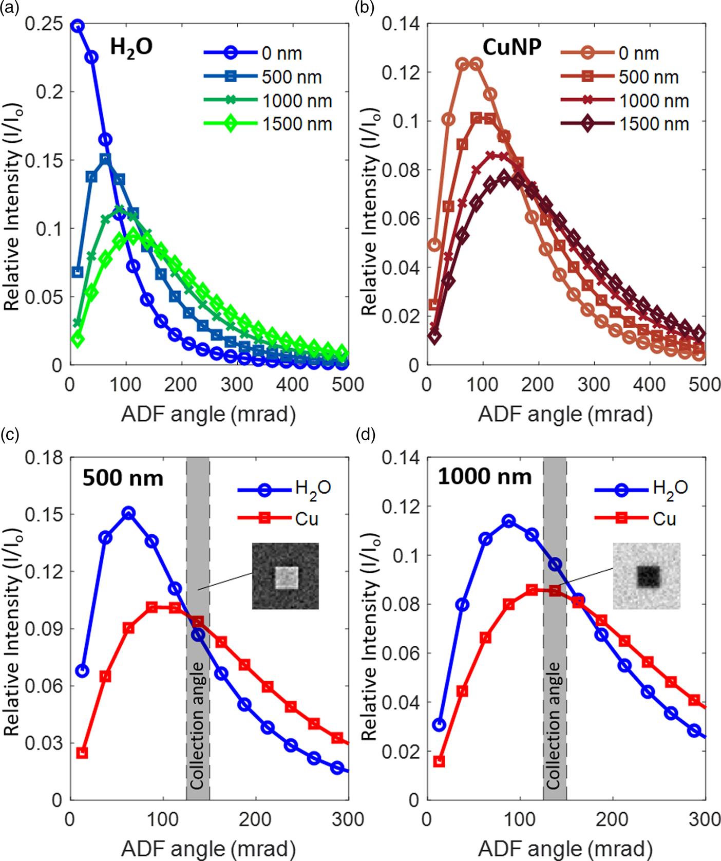
Fig. 5. The scattering angle of electrons passing through (a) water and (b) through a Cu nanocube + water. The intensity peak shifts toward higher angles with increasing liquid thickness for both water and Cu + water. (c and d) compare the relative intensities of electrons scattered by the Cu nanocube and by water layers that are 500 nm and 1,000 nm thick, respectively. At the fixed ADF collection angle of 125–150 mrad, the Cu nanocube in 500 nm of water is close to the transition between BF and DF contrast. In this case, the radially integrated intensity of the Cu (red) is still generally higher than that of the water (blue) and so, the nanocube appears bright with weak contrast against the background (inset in (c)). At the same ADF collection angle (125–150 mrad) with 1,000 nm of water, the Cu nanocube appears dark (inset in (d)), as the Cu intensity (red) is lower than the intensity by the water (blue). The relative intensity is obtained by dividing the scattering intensity (I) with the incident beam intensity (I 0).
Hence, we can use the scattering angle at which the BF contrast changes to DF contrast to estimate the liquid layer thickness. In our simulations for the Cu nanocubes, the ADF angle where the contrast is inverted has a linear relation with the liquid thickness t for thicknesses ranging from 0 up to 1,500 nm.
 $$t = \lpar {\beta -\beta_0} \rpar \times 10\;\lpar {\rm nm}/{\rm mrad}\rpar,$$
where β (mrad) is the ADF inner angle for which the BF to DF contrast shifts and occurs at the liquid thickness t (nm). β 0, the ADF inner angle where t = 0, can be measured without the liquid. The angle β 0 is a material-dependent scattering parameter; for instance, it is 75 mrad for Cu. Additional simulations of β 0 for different transition metals (from 55 mrad for Sc to 100 mrad for Au) indicate that β 0 correlates with the atomic scattering factor of the element (Supplementary Fig. S6). We also emphasize here that the range of liquid layer thicknesses of several hundred nanometers over which the contrast inversion occurs is especially relevant for LC-EM studies. In particular, it is important that we avoid situations where there is only a thin layer of liquid, especially for electrochemical studies. The highly restricted liquid volume, despite its benefits for acquiring clear images, does not represent a realistic electrochemical environment as it can lead to mass transport-limited behavior. The inverted contrast is an unambiguous indicator that we have at least liquid thicknesses of a few hundred nanometers in the cell and a reversal of the inverted contrast during experiments will imply bubble formation, which is often seen for gas evolving electrochemical reactions.
Conclusion
We have implemented a setup for the SEM using the LC geometry typically found in TEM holders where there are top-and-bottom silicon nitride windows. We show that this geometry has potential advantages for LC-SEM studies in terms of limiting beam-induced artifacts and the ability to use multiple detectors. Images acquired using BSEs largely retain high spatial resolution but suffer from decreasing signal-to-noise ratios with increasing liquid thicknesses. Images acquired using TEs show inverted contrast with thicker liquid layers and poorer spatial resolution but this configuration still allows the recording of reasonable images in moderately thick liquid layers. Hence, the two imaging modes can be used in a complementary manner. Moreover, MD simulations served to rationalize the imaging characteristics of the system. In particular, we explain the contrast inversion experimentally seen in the TE images by examining the angular profile of the scattered electrons. A specimen with a higher atomic number at the top membrane will scatter electrons to higher scattering angles as compared to the electrons that only pass through water. Therefore, at the range of detector collection angles that we typically have in experiments, the liquid appears bright and the particle appears dark. Furthermore, our results indicate that the collection angles at which the contrast inversion occurs can be used to estimate the liquid layer thickness, which is a very important parameter for LC-EM studies.
Supplementary material
To view supplementary material for this article, please visit https://doi.org/10.1017/S1431927620024769.
Acknowledgment
This work was supported by the European Research Council (ERC-725915, OPERANDOCAT). Funding by the Max-Planck-EPFL-Center for Molecular Nanoscience and Technology is also gratefully acknowledged.


 Open access