


Introduction
Transmission electron microscopy (TEM) is one of the most powerful characterization tools available to researchers studying nanoscale structures and phenomena. The unmatched spatial resolution of TEM, with the high degree of flexibility afforded by electromagnetic lenses and multipoles, and the large number of potential measurement channels have led to the development of many different operating modes for TEM. Scanning transmission electron microscopy (STEM), in particular, can perform a large number of different measurements, many of them simultaneously. This is because in STEM the electron probe is focused onto the sample surface and thus has a very small spatial extent, down to sub-atomic dimensions. After the STEM probe scatters from the sample, signals that can be measured include the forward diffracted electrons for various subsets of momenta, back-scattered electrons, X-rays, and secondary electrons generated inside the sample, and the energy loss spectroscopic signal. In this paper, we focus primarily on momentum-resolved measurements of the forward scattered electrons, especially those scattered elastically. Information on STEM development can be found in Pennycook & Nellist (Reference Pennycook and Nellist2011) and other TEM textbooks.
Figure 1 shows a momentum-resolved STEM experimental dataset measured from a dichalcogenide two-dimensional (2D) material. The STEM probe is formed by TEM condenser optics and possibly aberration-corrected. Next, it is focused on the sample surface, where it propagates through and scatters. After exiting the sample, the probe is magnified and measured on the detector plane in the far field. Note that in Figure 1, the diffraction images are displaced from each other in order not to overlap, but in reality all images are measured at the same detector position.
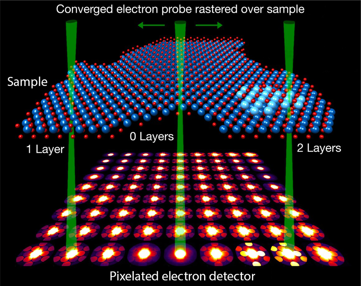
Fig. 1. Experimental 4D-STEM measurement of a dichalcogenide 2D material. Atomic map is inferred from the data, each diffraction pattern represents an average of 7 × 7 experimental images, green STEM probes are labeled for regions of the sample with one layer, vacuum, and two layers.
Each image in Figure 1 is an average of 49 adjacent probe images (in a 7 × 7 grid), where each image is approximately four megapixels. This gives a total dataset size of 420 GB, recorded in 164 s. Large-scale four-dimensional (4D)-STEM experiments such as this one have become possible because of two developments: high speed and efficient direct electron detectors, and the widespread availability of computational power.
The name “4D-STEM” refers to recording 2D images of a converged electron probe, over a 2D grid of probe positions. The resulting datasets are 4D, hence the term 4D-STEM, by which we mean all forms of scattering measurements where 2D images of a STEM probe are recorded, either in real or diffraction space, for a 2D grid of probe positions. This paper will review many different forms of 4D-STEM measurements, their history, and some recent developments. We will also discuss naming conventions, electron detector development, and simulation of 4D-STEM datasets.
Basics of 4D-STEM
Naming Conventions
The name “4D-STEM” is widely used in the literature, for example in Ophus et al. (Reference Ophus, Ercius, Sarahan, Czarnik and Ciston2014), Yang et al. (Reference Yang, Jones, Ryll, Simson, Soltau, Kondo, Sagawa, Banba, MacLaren and Nellist2015a), Ryll et al. (Reference Ryll, Simson, Hartmann, Holl, Huth, Ihle, Kondo, Kotula, Liebel and Müller-Caspary2016), Wang et al. (Reference Wang, Suyolcu, Salzberger, Hahn, Srot, Sigle and van Aken2018), Fatermans et al. (Reference Fatermans, den Dekker, Müller-Caspary, Lobato, OLeary, Nellist and Van Aert2018), Xu & LeBeau (Reference Xu and LeBeau2018), Hachtel et al. (Reference Hachtel, Idrobo and Chi2018), and Mahr et al. (Reference Mahr, Müller-Caspary, Ritz, Simson, Grieb, Schowalter, Krause, Lackmann, Soltau and Wittstock2019), though this name is far from universal. Note that it has also been used in the past to refer to combination STEM electron energy loss spectroscopy (EELS) and tomography, which also produces a 4D dataset. This technique however is typically referred to as “4D-STEM-EELS,” for example in Jarausch et al. (Reference Jarausch, Thomas, Leonard, Twesten and Booth2009), Florea et al. (Reference Florea, Ersen, Arenal, Ihiawakrim, Messaoudi, Chizari, Janowska and Pham-Huu2012), Goris et al. (Reference Goris, Turner, Bals and Van Tendeloo2014), and Midgley & Thomas (Reference Midgley and Thomas2014). Related terms for images of STEM diffraction patterns in common use from the literature include “convergent beam electron diffraction” (CBED), “microdiffraction,” “nanodiffraction,” “diffraction imaging,” and “diffractogram,” all of which refer to diffraction images of a converged electron probe. The term “ronchigram” is named for the “Ronchi test” for measuring aberrations of telescope mirrors and other optical elements, developed by Ronchi (Reference Ronchi1964). STEM probe diffraction measurements of aberrations using periodic objects were introduced by Cowley & Spence (Reference Cowley and Spence1979) and were referred to as ronchigrams by Cowley (Reference Cowley1986). Today the term usually refers to a diffraction image that is nearly in focus, typically recorded from an amorphous material.
Some of the earliest experiments that could be classified as 4D-STEM in the sense of this paper were those performed by Zaluzec (Reference Zaluzec2002) to measure the Lorentz deflection. Zaluzec referred to this method as “position resolved diffraction” (PRD) in accordance with earlier work where 2D diffraction patterns were recorded over a line scan. The term PRD is more often found in the X-ray diffraction literature, but can still be found in the TEM literature, for example in Chen et al. (Reference Chen, Weyland, Ercius, Ciston, Zheng, Fuhrer, D'Alfonso, Allen and Findlay2016). The similar term “spatially resolved diffractometry” was also used by Kimoto & Ishizuka (Reference Kimoto and Ishizuka2011), which they used to refer to virtual imaging in 4D-STEM. The term “momentum-resolved STEM” is also used by some authors, for example Müller-Caspary et al. (Reference Müller-Caspary, Duchamp, Rösner, Migunov, Winkler, Yang, Huth, Ritz, Simson and Ihle2018a).
Perhaps the most common alternative name for a 4D-STEM measurement in diffraction space is “scanning electron nanodiffraction”, used by Tao et al. (Reference Tao, Niebieskikwiat, Varela, Luo, Schofield, Zhu, Salamon, Zuo, Pantelides and Pennycook2009), Liu et al. (Reference Liu, Neish, Stokol, Buckley, Smillie, de Jonge, Ott, Kramer and Bourgeois2013), Gallagher-Jones et al. (Reference Gallagher-Jones, Ophus, Bustillo, Boyer, Panova, Glynn, Zee, Ciston, Mancia, Minor and Rodriguez2019), and many others. A similar descriptor used in many studies is “nanobeam electron diffraction” (NBED), used for example by Clément et al. (Reference Clément, Pantel, Kwakman and Rouvière2004), Hirata et al. (Reference Hirata, Guan, Fujita, Hirotsu, Inoue, Yavari, Sakurai and Chen2011), and Ozdol et al. (Reference Ozdol, Gammer, Jin, Ercius, Ophus, Ciston and Minor2015). The term “pixelated STEM” can also be found in the literature, for example in MacArthur et al. (Reference MacArthur, Pennycook, Okunishi, D'Alfonso, Lugg, Allen and Nellist2013). In addition to referring to pixelated STEM, Hachtel et al. (Reference Hachtel, Idrobo and Chi2018) also introduced the term “universal detector” to refer to virtual imaging in 4D-STEM.
One 4D-STEM application discussed extensively below is crystal orientation mapping. When using computer image processing methods to classify the crystal orientations automatically, this method is called “automated crystal orientation mapping” (ACOM), for example in Schwarzer & Sukkau (Reference Schwarzer and Sukkau1998), Seyring et al. (Reference Seyring, Song and Rettenmayr2011), Kobler et al. (Reference Kobler, Kashiwar, Hahn and Kübel2013), Izadi et al. (Reference Izadi, Darbal, Sarkar and Rajagopalan2017), and others.
Conventional STEM detectors record one value per pixel and usually have an annular (ring or circular) geometry. Common imaging modes include bright field (BF) where the detector is aligned with all or part of the unscattered probe, annular bright field (ABF) where a circle is removed from the center of the detector, and annular dark field (ADF) which selects an angular range of electrons scattered outside of the initial STEM probe. A very common STEM imaging mode is high-angle ADF (HAADF), which records only the incoherent signal of the thermal diffuse scattering (TDS) electrons, due to its easy interpretation (Pennycook & Nellist, Reference Pennycook and Nellist2011).
In this manuscript, we have chosen to use the general term of 4D-STEM in order to include imaging methodologies where the probe is recorded in real space, for example in (Nellist et al., Reference Nellist, Behan, Kirkland and Hetherington2006; Zaluzec, Reference Zaluzec2007; Etheridge et al., Reference Etheridge, Lazar, Dwyer and Botton2011).
Detector Development
The rise of popularity for 4D-STEM measurements is directly linked to the availability of high performance electron detector technology. Conventional STEM detectors for BF, ABF, ADF, and HAADF record only a single value per STEM probe position, and segmented detectors with 4–16 channels are used for differential measurements (Haider et al., Reference Haider, Epstein, Jarron and Boulin1994). Currently, the most common detector configuration recording full images in TEM is a charge coupled device (CCD) with digital readout, coupled with a scintillator, such as in Fan & Ellisman (Reference Fan and Ellisman1993) and De Ruijter (Reference De Ruijter1995). These detectors have good electron sensitivity, but typically have readout speeds limited to video rate (≤60 frames/s) and limited dynamic range. This makes CCDs ill-suited to 4D-STEM diffraction imaging, which requires readout speeds comparable with the STEM probe scanning rate (μs to ms timescales) and the ability to measure high-intensity signals such as the BF disk and low-intensity signals such as the high-angle scattered electrons simultaneously.
There are two primary routes to building detectors more suitable for 4D-STEM applications. The first detector type is monolithic active pixel sensors (APS), which are complementary metal–oxide–semiconductor (CMOS) chips with a sensitive doped epitaxial layer. When high energy electrons pass through this layer, many low energy electrons are generated, which diffuse toward sensor diodes where they are collected and read out using CMOS electronics, as described in Mendis et al. (Reference Mendis, Kemeny, Gee, Pain, Staller, Kim and Fossum1997), Dierickx et al. (Reference Dierickx, Meynants and Scheffer1997), and Milazzo et al. (Reference Milazzo, Leblanc, Duttweiler, Jin, Bouwer, Peltier, Ellisman, Bieser, Matis and Wieman2005). APS direct electron detectors have seen widespread deployment after being commercialized by several companies, for example in Ryll et al. (Reference Ryll, Simson, Hartmann, Holl, Huth, Ihle, Kondo, Kotula, Liebel and Müller-Caspary2016). See McMullan et al. (Reference McMullan, Faruqi, Clare and Henderson2014) for a performance comparison. APS detectors have very high sensitivities and fast readout speed, but relatively poor dynamic range. For high efficiency imaging, single “electron counting” is typically applied to images recorded with APS detectors (Li et al., Reference Li, Mooney, Zheng, Booth, Braunfeld, Gubbens, Agard and Cheng2013). This requires many pixels and relatively low electron doses in order to reduce the electron density recorded in each image to roughly less than 0.1 electrons per pixel per frame, since high densities prevent localization of individual electron strikes. If these conditions are met, electron counting can maximize the efficiency of 4D-STEM experiments, see Gallagher-Jones et al. (Reference Gallagher-Jones, Ophus, Bustillo, Boyer, Panova, Glynn, Zee, Ciston, Mancia, Minor and Rodriguez2019) for example. Note that because the design of APS detector pixels is relatively simple, these detectors typically contain a large number of pixels which decreases the electron density in each pixel.
The second kind of detector used in modern 4D-STEM experiments is a hybrid pixel array detector (PAD). In this type of detector, an array of photodiodes is bump bonded to an application-specific integrated circuit, described in Ansari et al. (Reference Ansari, Beuville, Borer, Cenci, Clark, Federspiel, Gildemeister, Gössling, Hara, Heijne, Jarron, Lariccia, Lisowski, Munday, Pal, Parker, Redaelli, Scampoli, Simak, Singh, Vallon-Hulth and Wells1989), Ercan et al. (Reference Ercan, Tate and Gruner2006), and Caswell et al. Reference Caswell, Ercius, Tate, Ercan, Gruner and Muller2009). PADs have been optimized for 4D-STEM experiments by using high-gain integration and counting circuitry in each pixel, giving single electron sensitivity, high dynamic range, and fast readout speeds (Tate et al., Reference Tate, Purohit, Chamberlain, Nguyen, Hovden, Chang, Deb, Turgut, Heron, Schlom, Ralph, Fuchs, Shanks, Philipp, Muller and Gruner2016). This detector has also been commercialized and used for many 4D-STEM experiments, for example in Jiang et al. (Reference Jiang, Chen, Han, Deb, Gao, Xie, Purohit, Tate, Park and Gruner2018).
Computational Methods
Almost every study described in this review uses computational imaging in some capacity. The digital recording of microscopy images and diffraction patterns quickly replaced the previously used film technology in no small part because it made it easy to use computers to analyze the resulting data. This review will not explicitly cover data recording, processing, and analysis methods. Instead we will provide a non-exhaustive list of code repositories that are currently being developed for 4D-STEM data analysis. These include: HyperSpy, pyXem, LiberTEM, Pycroscopy and py4DSTEM. Because so many of the 4D-STEM methods and technologies shown in this paper are being actively developed, we expect the software landscape to change considerably in the near future. We also want to encourage the vendors of commercial electron microscopes and detectors to allow full programmatic control of instrumentation in order to implement and optimize 4D-STEM experiments, and to use open source file formats for data and metadata.
Precession Electron Diffraction
Diffraction patterns from thicker samples can contain significant multiple scattering (i.e., dynamical diffraction). This leads to diffraction patterns where the average intensities of the Bragg disks are very uniform (i.e., structure factor details are lost), and a significant amount of fine structure generated inside each disk. Both of these effects can make indexing and quantitative intensity measurements of Bragg spots more difficult. One method to minimize multiple scattering is to collect an average diffraction pattern from many incident beam tilt directions, which is called “precession electron diffraction” (PED), or scanning-PED. Introduced by Vincent & Midgley (Reference Vincent and Midgley1994), PED uses deflection coils above and below the sample in order to tilt the angle of the beam incident on the sample, and then precess the beam through a range of azimuthal tilts. This “hollow cone” illumination integrates over excitation errors of different beams, which somewhat reduces dynamical scattering effects, and has found widespread application in electron crystallography (Midgley & Eggeman, Reference Midgley and Eggeman2015). As will be shown below, PED has been applied to many different 4D-STEM measurements. When combined with NBED measurements, this technique is sometimes referred to as “nanobeam precession electron diffraction”, as in Rouviere et al. (Reference Rouviere, Béché, Martin, Denneulin and Cooper2013).
Structure and Property Measurements
Virtual Imaging and Structure Classification
One of the most obvious uses of 4D-STEM diffraction imaging is the ability to use arbitrary “virtual” detectors by adding (or subtracting) some subset of the pixels in the diffraction patterns at each probe location. This removes one of the weaknesses of conventional STEM imaging; namely that a small number of bright and dark field detectors must be physically positioned at some angle from the optical axis, and cannot be changed relative to each other during the measurements. After a conventional STEM measurement, electrons within the scattering range are grouped together and can no longer be further separated by scattering angle. Note that nanodiffraction has been used for materials science investigations for a long time (Cowley, Reference Cowley1996). However, here we will review only 4D-STEM virtual imaging experiments, i.e., the sort of position-resolved nanodiffraction studies suggested by Zaluzec (Reference Zaluzec2003) or shown experimentally such as Fundenberger et al. (Reference Fundenberger, Morawiec, Bouzy and Lecomte2003), Lupini et al. (Reference Lupini, Chi, Kalinin, Borisevich, Idrobo and Jesse2015), and (Fatermans et al. (Reference Fatermans, den Dekker, Müller-Caspary, Lobato, OLeary, Nellist and Van Aert2018), and those which use such images to perform structural classification as in the schematic plotted in Figure 2a.
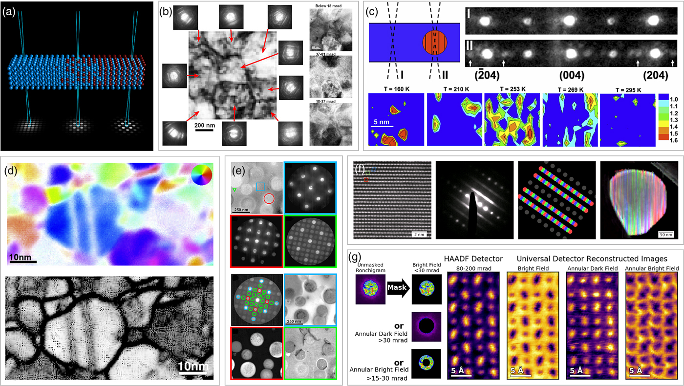
Fig. 2. Virtual imaging and classification in 4D-STEM. a: Schematic showing how properties such as local ordering can be directly determined from diffraction patterns. b: 4D-STEM experiment of Y-doped ZrO2 from Watanabe & Williams (Reference Watanabe and Williams2007), showing both diffraction patterns from different probe positions and images generated from virtual detectors in diffraction space. c: Nanoscale precipitate phase in La0.55Ca0.45MnO3 mapped from superlattice reflections, adapted from Tao et al. (Reference Tao, Niebieskikwiat, Varela, Luo, Schofield, Zhu, Salamon, Zuo, Pantelides and Pennycook2009). d: Top panel shows diffraction spot orientation and bottom panel shows correlation between adjacent diffraction patterns for a nanocrystalline Cu sample, adapted from Caswell et al. (Reference Caswell, Ercius, Tate, Ercan, Gruner and Muller2009). e: Top panel shows mean diffraction patterns from ROIs in real space, bottom panel shows virtual images generated from ROIs in diffraction space, from Gammer et al. (Reference Gammer, Ozdol, Liebscher and Minor2015). f: Images from left-to-right are an HRTEM image of cathode material at atomic resolution showing three stacking variants, mean diffraction pattern, virtual detectors, and output RGB image showing outputs of virtual detectors, from Shukla et al. (Reference Shukla, Ophus, Gammer and Ramasse2016). g: Virtual annular detectors at atomic resolution for a DyScO3 sample, from Hachtel et al. Reference Hachtel, Idrobo and Chi2018).
Figure 2 shows a 4D-STEM experiment imaging Y-doped ZrO2 performed by Watanabe & Williams (Reference Watanabe and Williams2007). Two methods to interpret such a measurement are both shown: either selecting diffraction patterns from different regions of constant contrast over the probe positions in real space, or generating a virtual detector from subsets of pixels in the reciprocal space diffraction pattern coordinate system. A similar experiment was performed by Schaffer et al. (Reference Schaffer, Gspan, Grogger, Kothleitner and Hofer2008), where first virtual dark field images were formed from regions of interest in the real space image along an interface. Then, virtual detectors were applied to resulting spots in the diffraction patterns to form improved dark field images and combined into a single RGB color map. Tao et al. (Reference Tao, Niebieskikwiat, Varela, Luo, Schofield, Zhu, Salamon, Zuo, Pantelides and Pennycook2009) used a similar approach, shown in Figure 2c, to map out the positions of a nanoscale precipitate phase in La0.55Ca0.45MnO3 as a function of sample temperature, using superlattice reflections. Zhang et al. (Reference Zhang, Ning, Busbee, Shen, Kiggins, Hua, Eaves, Davis, Shi and Shao2017) have also performed phase mapping of beam-sensitive battery cathode materials using diffraction mapping.
Advancing detector technology and increased stability of TEM instruments and sample stages has led to continual improvement in 4D-STEM diffraction mapping. Figure 2d shows the complex microstructure of a nanocrystalline copper sample mapped by Caswell et al. (Reference Caswell, Ercius, Tate, Ercan, Gruner and Muller2009) using both diffraction spot orientation mapping and correlation of adjacent diffraction patterns. Diffraction mapping at atomic resolution was demonstrated by Kimoto & Ishizuka (Reference Kimoto and Ishizuka2011), who recorded diffraction patterns from individual atomic columns in SrTiO3. Diffraction mapping capability with full control of the beam tilts before and after the sample was demonstrated by Koch et al. (Reference Koch, Özdöl and Ishizuka2012). Jones & Nellist (Reference Jones and Nellist2013) discussed the use of virtual detectors for imaging in 4D-STEM.
Figure 2e shows both virtual detectors in real space and diffraction space of a 4D-STEM measurement of an Fe–Al–Ni–Cr alloy measured by Gammer et al. (Reference Gammer, Ozdol, Liebscher and Minor2015). Zeng et al. (Reference Zeng, Zhang, Bustillo, Niu, Gammer, Xu and Zheng2015) used nanodiffraction mapping to characterize residual MoS2 products from nanosheets, after an electrochemical reaction in a liquid cell. Figure 2f shows virtual detectors applied to measure presence of three ordering variants of a battery cathode material by Shukla et al. (Reference Shukla, Ophus, Gammer and Ramasse2016). This example shows how 4D-STEM can in many cases obtain the same information as atomic-resolution HRTEM or conventional STEM images, but over a far larger field of view (FOV), a method used again in Shukla et al. (Reference Shukla, Ramasse, Ophus, Kepaptsoglou, Hage, Gammer, Bowling, Gallegos and Venkatachalam2018). An example of virtual annular detectors is shown in Figure 2g, from an experiment by (Hachtel et al., Reference Hachtel, Idrobo and Chi2018) imaging a DyScO3 sample at atomic resolution. Wang et al. (Reference Wang, Suyolcu, Salzberger, Hahn, Srot, Sigle and van Aken2018) have proposed methods for correcting sample drift both in STEM-EELS and 4D-STEM experiments. Li et al. (Reference Li, Dyck, Oxley, Lupini, McInnes, Healy, Jesse and Kalinin2019) have used machine learning methods to extract atomic-resolution defect information from 4D-STEM datasets.
More exotic property measurements are also possible with 4D-STEM experiments. Wehmeyer et al. (Reference Wehmeyer, Bustillo, Minor and Dames2018) used virtual apertures to measure thermal diffuse scattering between Bragg disks as a measurement of local temperature. Tao et al. (Reference Tao, Sun, Yin, Wu, Xin, Wen, Luo, Pennycook, Tranquada and Zhu2016) used 4D-STEM to study electronic liquid–crystal phase transitions and their microscopic origin, and Hou et al. (Reference Hou, Ashling, Collins, Krajnc, Zhou, Longley, Johnstone, Chater, Li, Coudert, Keen, Midgley, Mali, Chen and Bennett2018) used it to measure the degree of crystallinity in metal–organic-frameworks (MOFs). We expect that as pixelated detectors fall in price and larger amounts of computational power are available at the microscope, virtual imaging will become a very common operating mode for 4D-STEM. Commercial software to automate crystallographic phase mapping is already available, see for example Rauch et al. (Reference Rauch, Portillo, Nicolopoulos, Bultreys, Rouvimov and Moeck2010), combined with PED, which was described in a previous section of this paper. It has been used in various materials science studies, including, for example Brunetti et al. (Reference Brunetti, Robert, Bayle-Guillemaud, Rouviere, Rauch, Martin, Colin, Bertin and Cayron2011), who used it to understand Li diffusion in battery materials.
Crystalline and Semicrystalline Orientation Mapping
An important subset of structure classification for materials science is orientation mapping, and so we discuss it separately here. Electron backscatter diffraction using scanning electron microscopy (SEM) is the most commonly employed method to measure 2D maps of orientation distributions in crystalline materials, reviewed in Wright et al. (Reference Wright, Nowell and Field2011). Schwarzer & Sukkau (Reference Schwarzer and Sukkau1998) also reviewed ACOM methods for measuring maps of crystalline grain orientations in SEM and suggested their future applicability to TEM experiments in order to increase resolution of orientation maps. In TEM diffraction imaging, orientation of a crystalline sample can be determined by either fitting Kikuchi diffraction patterns (Kikuchi, Reference Kikuchi1928) plotted in Figure 3a, or by direct indexing of the scattered Bragg spots or disks (Schwarzer, Reference Schwarzer1990) as shown in Figure 3b. Bragg spot indexing in 4D-STEM is essentially a form of selected area diffraction, where the “area” selected is the region illuminated by the STEM probe. Both methods are qualitatively similar, but each has strengths and weaknesses. Generally, spot indexing is better for thinner specimens, while Kikuchi diffraction performs better for thicker samples (as formation of Kikuchi bands relies on a sufficient diffuse scattering being present). Additionally, the orientation precision tends to be higher for Kikuchi diffraction due to the sharpness of the features measured, but it can fail in regions of high local deformation when the line signal becomes too delocalized. See Zaefferer (Reference Zaefferer2000), Zaefferer (Reference Zaefferer2011), and Morawiec et al. (Reference Morawiec, Bouzy, Paul and Fundenberger2014) for further information comparing these methods.
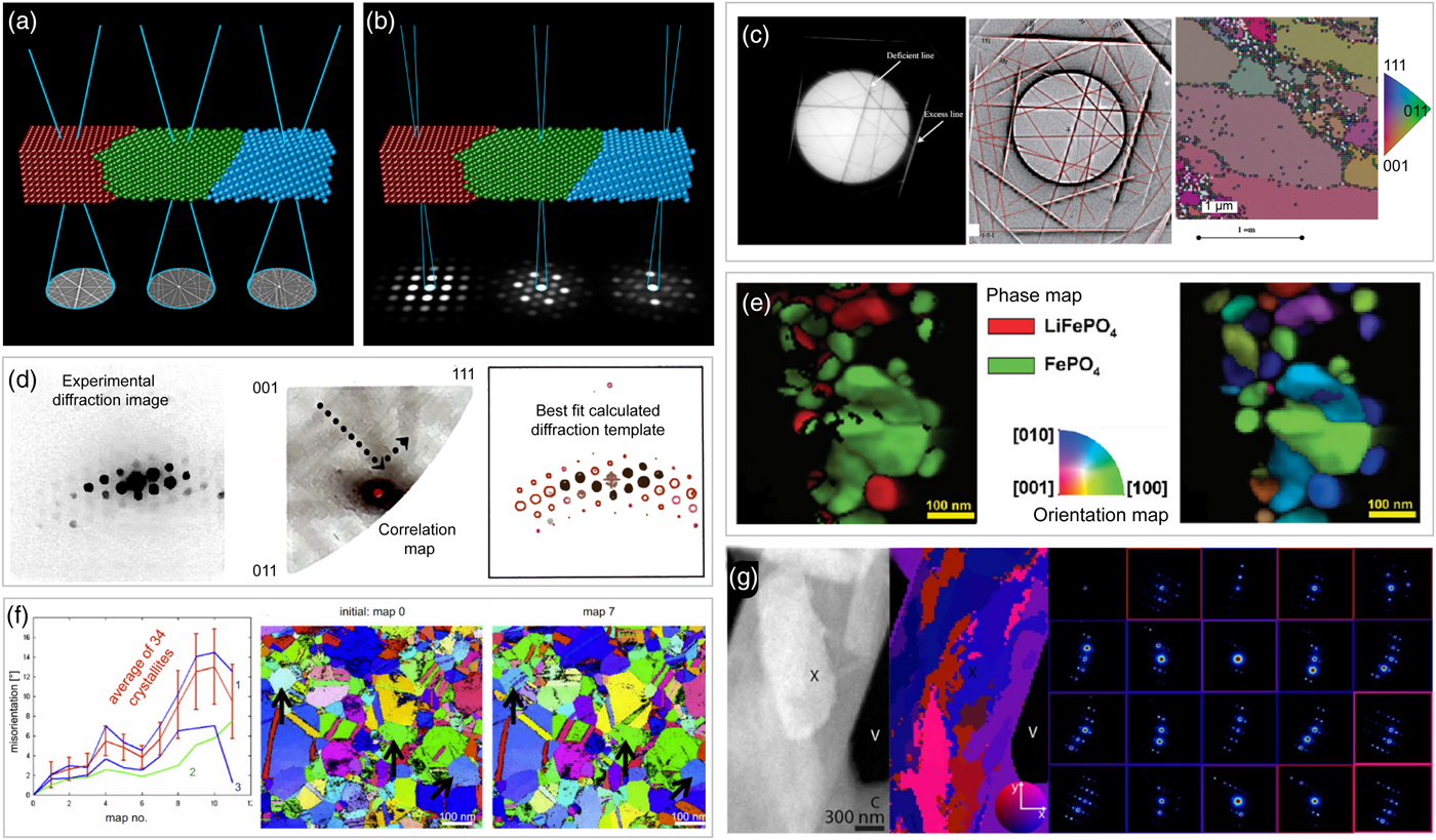
Fig. 3. Orientation mapping in 4D-STEM, using (a) Kikuchi patterns, or (b) Bragg disk diffraction. c: Kikuchi patterns indexing and orientation map of aluminum, adapted from Fundenberger et al. (Reference Fundenberger, Morawiec, Bouzy and Lecomte2003). d: Orientation of Bragg disk pattern estimated with template matching, and resulting correlation scores for all orientations, by Rauch & Dupuy (Reference Rauch and Dupuy2005). e: Simultaneous phase and orientation determination for LiFePO4, from Brunetti et al. (Reference Brunetti, Robert, Bayle-Guillemaud, Rouviere, Rauch, Martin, Colin, Bertin and Cayron2011). f: In-situ orientation mapping of nanocrystalline Au during a mechanical test, from Kobler et al. (Reference Kobler, Kashiwar, Hahn and Kübel2013). g: Orientation map of a biological peptide crystal, from Gallagher-Jones et al. (Reference Gallagher-Jones, Ophus, Bustillo, Boyer, Panova, Glynn, Zee, Ciston, Mancia, Minor and Rodriguez2019).
Early implementations of orientation mapping in TEM did not have the computer memory or disk space to record every diffraction pattern for later analysis. Instead, patterns were typically acquired and indexed online. An early implementation of orientation mapping using Kikuchi patterns was developed by Fundenberger et al. (Reference Fundenberger, Morawiec, Bouzy and Lecomte2003). Figure 3c shows one of these measurements, how it is high pass filtered and then fitted with an indexed line pattern, and finally an output orientation map for a deformed aluminum sample. As shown in Figure 2b, Watanabe & Williams (Reference Watanabe and Williams2007) performed a very early 4D-STEM experiment where a Kikuchi diffraction orientation map could be constructed from a 4D-STEM scan. The Kikuchi method has been applied in many materials science studies, for example to a TiAl alloy by Dey et al. (Reference Dey, Morawiec, Bouzy, Hazotte and Fundenberger2006), to cold-rolling of Ti by Bozzolo et al. (Reference Bozzolo, Dewobroto, Wenk and Wagner2007), to ferroelectric domains by MacLaren et al. (Reference MacLaren, Villaurrutia and Peláiz-Barranco2010), and others. Note that Kikuchi pattern orientation mapping can also be performed in an SEM; this method has been demonstrated by Trimby (Reference Trimby2012) and Brodusch et al. (Reference Brodusch, Demers and Gauvin2013).
An example of orientation mapping using Bragg spots is shown in Figure 3d from Rauch & Dupuy (Reference Rauch and Dupuy2005). They introduced a fast “template matching” procedure, where the diffraction patterns are pre-computed for each orientation of a given material, and then, as shown in Figure 3d, a correlation score is computed for each experimental pattern. This method can be fully automated, and can also generate an estimate of the measurement confidence using the maximum correlation score (Rauch et al., Reference Rauch, Portillo, Nicolopoulos, Bultreys, Rouvimov and Moeck2010). Combined with PED, phase and orientation mapping has been commercialized and widely deployed (Darbal et al., Reference Darbal, Gemmi, Portillo, Rauch and Nicolopoulos2012). A review of these methods for automated orientation mapping is given in Rauch & Véron (Reference Rauch and Véron2014). The combination of scanning diffraction measurements, PED, and sample tilt to create 3D orientation tomographic reconstructions was shown by Eggeman et al. (Reference Eggeman, Krakow and Midgley2015). Other extensions to orientation mapping include applying principal component analysis and machine learning techniques to orientation measurements in 4D-STEM datasets, for example in studies by Sunde et al. (Reference Sunde, Marioara, van Helvoort and Holmestad2018) and Ånes et al. (Reference Ånes, Andersen and van Helvoort2018).
Figure 3e shows simultaneously recorded phase and orientation maps for LiFePO4, from an experiment performed by Brunetti et al. (Reference Brunetti, Robert, Bayle-Guillemaud, Rouviere, Rauch, Martin, Colin, Bertin and Cayron2011) using PED and the spot matching method. These experiments were used to determine the correct transformation pathway model for this material, thus highlighting the usefulness of “plug and play” methods for TEM phase and orientation mapping. Kobler et al. (Reference Kobler, Kashiwar, Hahn and Kübel2013) extended ACOM experiments to in-situ mechanical testing measurements of nanocrystalline Au, with an example shown in Figure 3f. In this example, the misorientation angle of many grains was measured as a function of the loading force. These and many other statistics can be obtained simultaneously using time-resolved ACOM. Other examples of in-situ studies include: Idrissi et al. (Reference Idrissi, Kobler, Amin-Ahmadi, Coulombier, Galceran, Raskin, Godet, Kübel, Pardoen and Schryvers2014), Garner et al. (Reference Garner, Gholinia, Frankel, Gass, MacLaren and Preuss2014), Bufford et al. Reference Bufford, Abdeljawad, Foiles and Hattar2015), Izadi et al. Reference Izadi, Darbal, Sarkar and Rajagopalan2017), Guo & Thompson (Reference Guo and Thompson2018), and others. An extreme example of orientation mapping was recently published by Bruma et al. (Reference Bruma, Santiago, Alducin, Plascencia Villa, Whetten, Ponce, Mariscal and José-Yacamán2016), who analyzed beam-induced rotation of 102-atom Au clusters.
Orientation maps can also be determined for semicrystalline materials, such as small molecule assemblies or polymers. One such example was shown by Panova et al. (Reference Panova, Chen, Bustillo, Ophus, Bhatt, Balsara and Minor2016), who mapped the degree of crystallinity and orientation of a polymer sample. Bustillo et al. (Reference Bustillo, Panova, Chen, Takacs, Ciston, Ophus, Balsara and Minor2017) extended this method to include multiple soft matter samples, including organic semiconductors. Mohammadi et al. (Reference Mohammadi, Zhao, Meng, Qu, Zhang, Zhao, Mei, Zuo, Shukla and Diao2017) have also performed orientation mapping of semiconducting polymers using 4D-STEM. They employed a statistical approach to measure the angular deviation of the π − π stacking direction over a very large FOV. Orientation mapping has even been applied to peptide crystals, in the study by Gallagher-Jones et al. (Reference Gallagher-Jones, Ophus, Bustillo, Boyer, Panova, Glynn, Zee, Ciston, Mancia, Minor and Rodriguez2019) which analyzed small magnitude ripples, as shown in Figure 3g. The ability to use very low electron currents, small convergence angle (large real space probe size) or highly defocused STEM probes, and adjustable step size between adjacent measurements are key advantages of 4D-STEM mapping of radiation-sensitive materials. For such materials, the maximum obtainable spatial resolution can be achieved by careful tuning of the experimental parameters and dose in order to measure structural properties such as orientation to the required precision, balanced against the density of probe positions. For a review of electron beam damage mechanisms and how they can be minimized, we direct readers to Egerton (Reference Egerton2019).
Strain Mapping
Many functional materials possess a large degree of local variation in lattice parameter (or for amorphous or semicrystalline materials, variation in local atomic spacing), which can have a large effect on the materials' electronic and mechanical properties. TEM can measure these local strains with both good precision and high resolution using CBED patterns, NBED, HRTEM, and dark field holography (Hÿtch & Minor, Reference Hÿtch and Minor2014). Strain measurements with CBED (or large angle CBED, i.e., LACBED) usually refers to using precision measurements of the higher order Laue zone (HOLZ) features of the diffraction pattern of a converged electron probe to directly probe the local lattice parameter (Jones et al., Reference Jones, Rackham and Steeds1977). While in principle this is compatible with 4D-STEM measurements, these measurements typically require detailed calculations to interpret the CBED patterns (Rozeveld & Howe, Reference Rozeveld and Howe1993), samples thin enough for the kinematic approximation to hold (Zuo, Reference Zuo1992), and usually a favorable symmetry of the CBED pattern along the available sample orientations (Kaufman et al., Reference Kaufman, Pearson and Fraser1986). Nevertheless, CBED HOLZ measurements of local strain are widely used, especially for single crystalline semiconductor samples such as in Clément et al. (Reference Clément, Pantel, Kwakman and Rouvière2004) or Zhang et al. (Reference Zhang, Istratov, Weber, Kisielowski, He, Nelson and Spence2006).
In contrast, strain measurements from NBED experiments are usually simpler to interpret. Because the local strain precision does not depend on directly measuring the atomic column positions, the FOV is essentially unlimited and almost any sample and orientation can be used (Béché et al., Reference Béché, Rouviere, Clément and Hartmann2009). A schematic of an NBED strain measurement is shown in Figure 4a, illustrating the inverse relationship between interatomic distance and diffraction disk spacing.
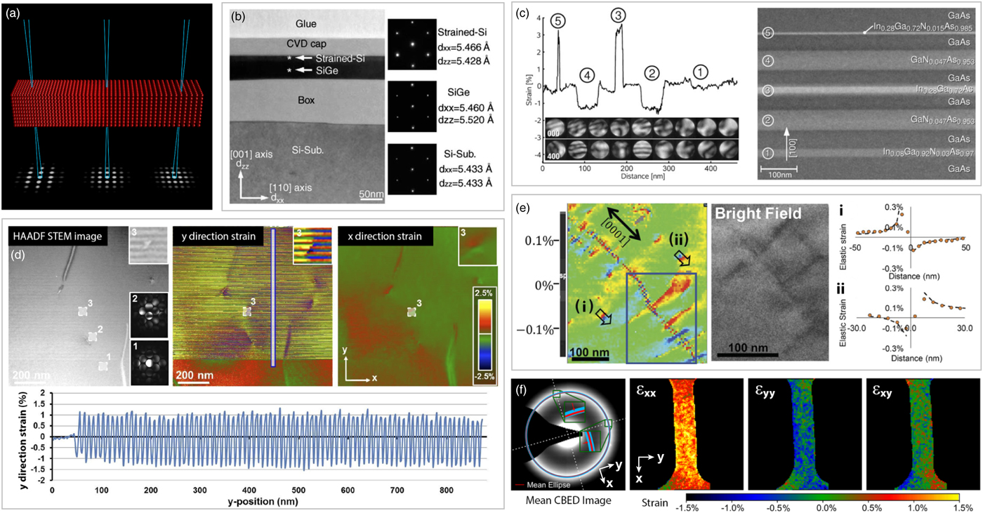
Fig. 4. Strain measurements in 4D-STEM. a: Schematic showing how diffraction disk spacing varies inversely with interatomic distances. b: Precise lattice parameter determination in multilayer semiconductor sample, from Usuda et al. (Reference Usuda, Mizuno, Tezuka, Sugiyama, Moriyama, Nakaharai and Takagi2004). c: Strain measurements in the presence of large variations of diffraction disk contrast patterns, adapted from Müller et al. (Reference Müller, Rosenauer, Schowalter, Zweck, Fritz and Volz2012a). d: Strain maps with a large FOV, from Ozdol et al. (Reference Ozdol, Gammer, Jin, Ercius, Ophus, Ciston and Minor2015). e: Strain map from a polycrystalline sample, with strain distributions of single distributions plotted, from Rottmann & Hemker (Reference Rottmann and Hemker2018). f: Strain measurements from a metallic glass mechanical testing sample, adapted from Gammer et al. (Reference Gammer, Ophus, Pekin, Eckert and Minor2018).
The NBED strain measurement technique was first introduced by Usuda et al. (Reference Usuda, Mizuno, Tezuka, Sugiyama, Moriyama, Nakaharai and Takagi2004), applied to the sample shown in Figure 4b. To improve the spatial resolution of the strain measurements, the STEM probe size must be decreased by opening up the convergence semiangle of the probe-forming aperture in diffraction space. This however will introduce unwanted fine structure contrast in the diffraction disks for thicker samples, due to excitation errors and dynamical diffraction, shown in experiments by Müller et al. (Reference Müller, Rosenauer, Schowalter, Zweck, Fritz and Volz2012a) and plotted in Figure 4c. In that study, the authors focused on making their measurements as accurate and robust as possible for the large variation in the diffraction disk intensity patterns, using circular pattern recognition. This was also the focus of the work by Pekin et al. (Reference Pekin, Gammer, Ciston, Minor and Ophus2017), who analyzed using different correlation methods where a vacuum reference probe was compared with experimental and synthetic diffraction patterns. Other authors have analyzed the accuracy of NBED strain measurements including Williamson et al. (Reference Williamson, van Dooren and Flanagan2015), Grieb et al. (Reference Grieb, Krause, Mahr, Zillmann, Müller-Caspary, Schowalter and Rosenauer2017), and Grieb et al. (Reference Grieb, Krause, Schowalter, Zillmann, Sellin, Müller-Caspary, Mahr, Mehrtens, Bimberg and Rosenauer2018), or the influence of artifacts such as elliptic distortion by Mahr et al. (Reference Mahr, Müller-Caspary, Ritz, Simson, Grieb, Schowalter, Krause, Lackmann, Soltau and Wittstock2019).
Many researchers have applied NBED to materials science studies, including Liu et al. (Reference Liu, Li, Pandey, Benistant, See, Zhou, Hsia, Schampers and Klenov2008), Sourty et al. (Reference Sourty, Stanley and Freitag2009), Favia et al. (Reference Favia, Popovici, Eneman, Wang, Bargallo-Gonzalez, Simoen, Menou and Bender2010), Uesugi et al. (Reference Uesugi, Hokazono and Takeno2011), and Haas et al. (Reference Haas, Thomas, Jouneau, Bernier, Meunier, Ballet and Rouvière2017). Very recent studies, including Han et al. (Reference Han, Nguyen, Cao, Cueva, Xie, Tate, Purohit, Gruner, Park and Muller2018), have even extended strain measurements to heterostructures in very weakly scattering 2D materials. Comparisons of the strengths and weaknesses between NBED and other TEM strain measurement methods have been performed by Favia et al. (Reference Favia, Gonzales, Simoen, Verheyen, Klenov and Bender2011) and Cooper et al. (Reference Cooper, Denneulin, Bernier, Béché and Rouvière2016).
4D-STEM strain measurements have an inherent trade-off between resolution in real space and reciprocal space. A larger convergence angle will generate a smaller probe, giving better resolution in real space. However, this will also decrease the strain measurement precision. By decreasing the convergence angle, the STEM probe size in real space will be increased. A 4D-STEM measurement under these conditions will have lower spatial resolution but improved strain precision, due to averaging the strain measurement over a larger volume. However, the STEM probes can also be spaced further apart than the spatial resolution limit. Thus the only limit on FOV size is the speed of the detector readout. By using the millisecond readout times possible with direct electron detectors, the FOV can be increased as demonstrated by Müller et al. (Reference Müller, Ryll, Ordavo, Ihle, Strüder, Volz, Zweck, Soltau and Rosenauer2012b). Another example of the large FOV possible with 4D-STEM strain measurements is plotted in Figure 4d, by Ozdol et al. (Reference Ozdol, Gammer, Jin, Ercius, Ophus, Ciston and Minor2015). In this work, the sample region scanned was almost 1 µm2, and the measurement was found to be extremely consistent across the FOV for a well-controlled multilayer semiconductor sample. 4D-STEM strain measurements have also been performed in situ, for example in Pekin et al. (Reference Pekin, Gammer, Ciston, Ophus and Minor2018).
One notable extension to NBED strain measurements in 4D-STEM is the use of PED to enhance the measurement precision. Heterogeneity in the diffraction disks is typically the limiting factor in the measurement precision, for example as shown in measurements by Pekin et al. (Reference Pekin, Gammer, Ciston, Minor and Ophus2017). PED can improve precision of 4D-STEM strain measurements, shown by Rouviere et al. (Reference Rouviere, Béché, Martin, Denneulin and Cooper2013), Vigouroux et al. (Reference Vigouroux, Delaye, Bernier, Cipro, Lafond, Audoit, Baron, Rouvière, Martin and Chenevier2014), and Reisinger et al. (Reference Reisinger, Zalesak, Daniel, Tomberger, Weiss, Darbal, Petrenec, Zechner, Daumiller, Ecker, Sartory and Keckes2016) for multilayer semiconductor devices. The improvement in precision for PED strain measurements was also analyzed in detail by Mahr et al. (Reference Mahr, Müller-Caspary, Grieb, Schowalter, Mehrtens, Krause, Zillmann and Rosenauer2015). PED was also used to measure strain maps for complex polycrystalline materials by Rottmann & Hemker (Reference Rottmann and Hemker2018), including high precision measurements of strain in low angle grain boundaries and even single dislocations. These experiments are shown in Figure 4e. Mahr et al. (Reference Mahr, Müller-Caspary, Grieb, Schowalter, Mehrtens, Krause, Zillmann and Rosenauer2015) also proposed the use of a patterned probe-forming aperture to improve strain measurement precision, specifically the addition of a cross which divides the probe into four quarters. Guzzinati et al. (Reference Guzzinati, Ghielens, Mahr, Béché, Rosenauer, Calders and Verbeeck2019) have also used a patterned annular ring aperture to generate Bessel beam STEM probes, which improves the measure of strain precision.
In addition to crystalline materials, amorphous and semi-crystalline materials can also exhibit local deviations away from the mean atomic spacing or average layer stacking distance respectively. Ebner et al. (Reference Ebner, Sarkar, Rajagopalan and Rentenberger2016) demonstrated that it was possible to measure this variation in a metallic glass. By combining this method with 4D-STEM performed with a fast detector, Gammer et al. (Reference Gammer, Ophus, Pekin, Eckert and Minor2018) were able to map the strain distribution in a metallic glass sample machined into a dogbone geometry for in-situ mechanical testing. Figure 4f shows an intermediate time step where the sample is under mechanical load; the mean CBED image shows the characteristic “amorphous ring” which was fit for every probe position to determine the relative strain maps, referenced to the unloaded sample.
Finally we note that alternative detector technologies have also been employed to measure strain maps. For example, Müller-Caspary et al. (Reference Müller-Caspary, Oelsner and Potapov2015) used a delay-line detector to map strain in field effect transistors fabricated from silicon.
Medium Range Order Measurement Using Fluctuation Electron Microscopy
Many interesting materials in materials science are not crystalline, and the tendency of some materials to form structurally disordered or “glassy” phases has been discussed for a long time (Phillips, Reference Phillips1979). The degree of medium range order (MRO) in glassy materials can be measured using “fluctuation electron microscopy” (FEM), as suggested by Treacy & Gibson (Reference Treacy and Gibson1996) and drawn schematically in Figure 5a. Figure 5b shows FEM measurements of α-Ge performed using converged electron probes, shown by Rodenburg (Reference Rodenburg1999). This experiment demonstrates the basic principle of FEM: when the probe is focused to roughly the same length scale as the atomic ordering length of the sample, “speckles” appear in the diffraction pattern. When the probe is defocused (made larger in the sample plane), these speckles fade away. Measuring the intensity variance as a function of scattering angle (e.g., the ring shown in Fig. 5b) and probe size can yield information about the degree of MRO and the length scales where it is present in a sample. Voyles & Muller (Reference Voyles and Muller2002) showed that STEM has significant measurement advantages over other TEM operating modes for FEM, one being the ability to easily adjust the probe size, for “variable resolution” (VR)-FEM. Some of their FEM measurements of α-Si are shown in Figure 5c. By using VR-FEM, the characteristic length scale of the MRO can be determined, such as in the example plotted in Figure 5d from Bogle et al. (Reference Bogle, Nittala, Twesten, Voyles and Abelson2010). VR-FEM has been used to study many other materials, for example metallic glasses in Hwang et al. (Reference Hwang, Melgarejo, Kalay, Kalay, Kramer, Stone and Voyles2012) and α-Si in Hilke et al. (Reference Hilke, Kirschbaum, Hieronymus-Schmidt, Radek, Bracht, Wilde and Peterlechner2019).

Fig. 5. FEM in STEM. a: Schematic showing how structural disorder generates the speckle pattern used in FEM. b: FEM measurements of α-Ge, adapted from Rodenburg (Reference Rodenburg1999). c: FEM measurements of α-Si using a variable STEM probe size, from Voyles & Muller (Reference Voyles and Muller2002). d: Characteristic length scale measurements of MRO in α-Si, from Bogle et al. (Reference Bogle, Nittala, Twesten, Voyles and Abelson2010). e: Example of diffraction patterns of a Cu–Zr metallic glass, measurement of local MRO symmetry using angular cross-correlation functions, adapted from Liu et al. (Reference Liu, Neish, Stokol, Buckley, Smillie, de Jonge, Ott, Kramer and Bourgeois2013).
A large amount of scattering information is collected when performing a 4D-STEM FEM experiment. In addition to estimating the degree of MRO, it can also be used to measure the density of atomic clusters with different rotational symmetry. Examples of diffraction images of individual atomic clusters are shown in (Hirata et al., Reference Hirata, Guan, Fujita, Hirotsu, Inoue, Yavari, Sakurai and Chen2011). Figure 5e shows a measurement of Cu–Zr metallic glass where Liu et al. (Reference Liu, Neish, Stokol, Buckley, Smillie, de Jonge, Ott, Kramer and Bourgeois2013) used angular cross-correlation functions of the diffraction patterns to measure the length scale and density of all rotational orders up to 12-fold symmetry. By comparing these measurements with atomic models, they concluded that icosahedral ordering was the dominant structural motif due to strong measurements of two, six, and tenfold symmetries. Figure 5e also shows spatial maps of these features. A follow up study by Liu et al. (Reference Liu, Lumpkin, Petersen, Etheridge and Bourgeois2015) used simulations to test the interpretation of angular cross-correlation functions. Pekin et al. (Reference Pekin, Gammer, Ciston, Ophus and Minor2018) have extended this method to in-situ heating experiments for a Cu–Zr–Al metallic glass, and Im et al. (Reference Im, Chen, Johnson, Zhao, Yoo, Park, Wang, Muller and Hwang2018) have measured the degree of local ordering for different angular symmetries in a Zr–Co–Al glass, both using modern 4D-STEM cameras capable of recording a large amount of data with good statistics. A review of TEM measurements of heterogeneity in metallic glasses has been published by Tian & Volkert (Reference Tian and Volkert2018).
Position-Averaged Convergent Beam Electron Diffraction
Quantitative CBED has a long history in TEM research, since under the right imaging conditions various sample parameters such as thickness can be determined with high precision (Steeds, Reference Steeds1979). However, conventional CBED experiments can require precise tilting of the sample, a minimum sample thickness to be effective, and sometimes require simulations to interpret the results. A recent related diffraction imaging method was introduced by LeBeau et al. (Reference LeBeau, Findlay, Wang, Jacobson, Allen and Stemmer2009), called position-averaged convergent beam electron diffraction (PACBED). In this technique, shown schematically in Figure 6a, the diffraction patterns of an atomic-scale (large convergence angle) probe are incoherently averaged as the beam is scanned over the sample surface. As long as the averaging is performed over at least one full unit cell of a crystalline sample, PACBED images form a fingerprint signal, which can be used to determine sample parameters such as thickness, tilt, or sample polarization with high precision, by comparing directly with simulated PACBED images, as shown by LeBeau et al. (Reference LeBeau, Findlay, Allen and Stemmer2010). Figure 6b shows one of their experiments, thickness determination of a PbWO4 sample over a large range of sample thicknesses, using comparisons with Bloch wave simulations. PACBED thickness measurements have found widespread application in STEM experiments, for example in Zhu et al. (Reference Zhu, Radtke and Botton2012), Hwang et al. (Reference Hwang, Zhang, DAlfonso, Allen and Stemmer2013), Yankovich et al. (Reference Yankovich, Berkels, Dahmen, Binev, Sanchez, Bradley, Li, Szlufarska and Voyles2014), and Grimley et al. (Reference Grimley, Schenk, Mikolajick, Schroeder and LeBeau2018).
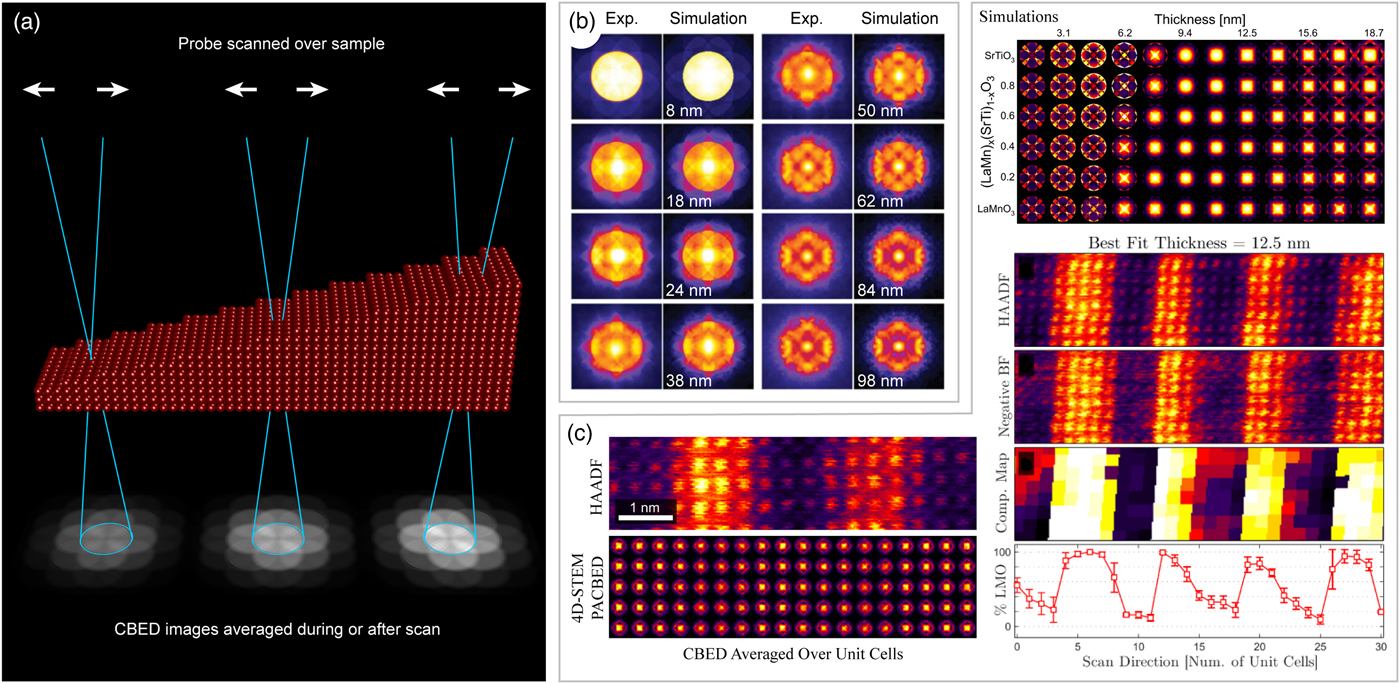
Fig. 6. Position averaged convergent beam electron diffraction (PACBED). a: Schematic showing how thickness strongly modules PACBED images. b: Thickness fitting of PbWO4 using PACBED, adapted from LeBeau et al. (Reference LeBeau, Findlay, Allen and Stemmer2010). c: Composition fitting of LaMnO3–SrTiO3 multilayers using PACBED, adapted from Ophus et al. (Reference Ophus, Ercius, Huijben and Ciston2017a).
Ophus et al. (Reference Ophus, Ercius, Sarahan, Czarnik and Ciston2014) showed that 4D-STEM datasets of crystalline samples can be adapted to form PACBED images. First, the lattice is fit to either a simultaneously recorded ADF image, or a virtual image from the 4D-STEM dataset, and then each probe is assigned to a given unit cell. Averaging these patterns produces a single unit cell-scale PACBED image. An example of this procedure is shown in Figure 6c, where PACBED was used to determine the local composition of a LaMnO2–SrTiO3 multilayer stack in a STEM instrument without aberration correction, from Ophus et al. (Reference Ophus, Ercius, Huijben and Ciston2017a). Note that as seen in the HAADF images, the STEM probe resolution was not sufficient to resolve individual atomic columns inside the perovskite unit cell, showing that PACBED does not require high resolution STEM imaging. PACBED has also been used to measure unit cell distortion in double-unit-cell perovskites by Nord et al. (Reference Nord, Ross, McGrouther, Barthel, Moreau, Hallsteinsen, Tybell and MacLaren2018). A recently developed method to augment PACBED fitting was shown by Xu & LeBeau (Reference Xu and LeBeau2018), who used a convolutional neural network to automatically align and analyze the images. They showed that this approach can be quite robust to noise and can process PACBED images very quickly, which is important since the dataset sizes can be very large.
Phase Contrast Imaging
As described above, the most popular STEM imaging method for samples in materials science is HAADF measurements. However, HAADF is not very sensitive to weakly scattering samples such as low atomic number materials or 2D materials (Ophus et al., Reference Ophus, Ciston, Pierce, Harvey, Chess, McMorran, Czarnik, Rose and Ercius2016). A more dose-efficient alternative is phase contrast imaging, which is therefore more suitable for these cases. Methods for measuring the phase shift imparted to an electron wave by a sample in a STEM experiment were first discussed by Rose (Reference Rose1974), Dekkers and De Lang (Reference Dekkers and De Lang1974), and Rose (Reference Rose1977). These STEM phase contrast imaging methods and some modern 4D-STEM extensions will be discussed in this section.
Differential Phase Contrast
When a converged electron probe has a similar size to the length scale of the variations of a sample's electric field (gradient of the electrostatic potential), it will be partially or wholly deflected. Figure 7a shows an ideal probe deflection in the presence of a phase gradient with infinite extent. This momentum change imparted to the STEM probe can be measured in diffraction space using a variety of detector configurations, originally by using a difference signal between different segmented detectors that do not have rotational symmetry (Dekkers & De Lang, Reference Dekkers and De Lang1974), a method long known in optical microscopy (Françon, Reference Françon1954). The differential phase contrast (DPC) imaging technique implemented on segmented detectors (Haider et al., Reference Haider, Epstein, Jarron and Boulin1994) was steadily improved all the way to atomic resolution imaging (Shibata et al., Reference Shibata, Findlay, Kohno, Sawada, Kondo and Ikuhara2012). More information on the theory of DPC can be found in Lubk & Zweck (Reference Lubk and Zweck2015). Note that in Lorentz imaging modes in TEM, DPC measurements are also sensitive to the magnetic field of the sample (Chapman et al., Reference Chapman, McFadyen and McVitie1990).
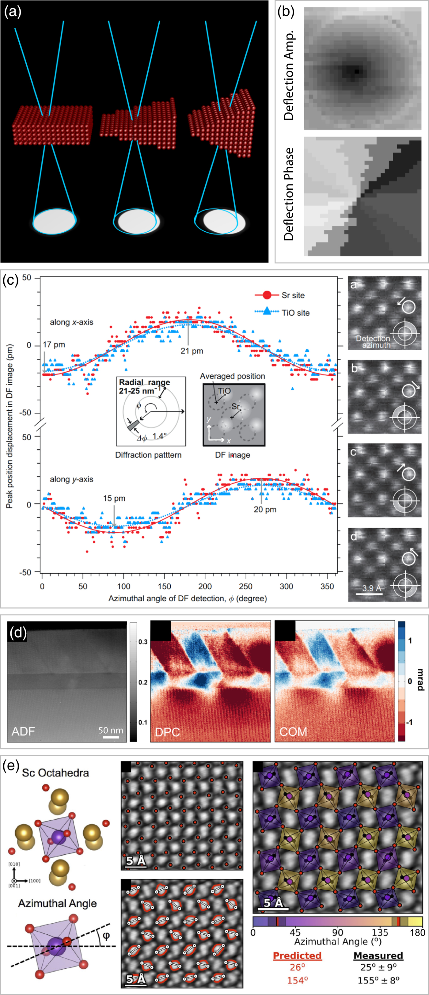
Fig. 7. DPC measurements in STEM. a: STEM probe deflection from ideal phase wedges with different slopes. b: Lorentz field deflection measurement of a permalloy microdot, adapted from Zaluzec (Reference Zaluzec2002). c: Shift of peak positions in SrTiO3, from Kimoto & Ishizuka (Reference Kimoto and Ishizuka2011). d: Simultaneous measurements of ADF image, DPC signal from segments, and COM DPC signal from a multilayer stack, adapted from Tate et al. (Reference Tate, Purohit, Chamberlain, Nguyen, Hovden, Chang, Deb, Turgut, Heron, Schlom, Ralph, Fuchs, Shanks, Philipp, Muller and Gruner2016). e: DPC measurements of octahedral tilts in DyScO3, from Hachtel et al. (Reference Hachtel, Idrobo and Chi2018).
As discussed by Waddell & Chapman (Reference Waddell and Chapman1979), Pennycook et al. (Reference Pennycook, Lupini, Yang, Murfitt, Jones and Nellist2015), and Yang et al. (Reference Yang, Pennycook and Nellist2015b), use of fixed segmented detectors for DPC measurements reduces the information transfer efficiency of many spatial frequencies. One way to avoid this problem is to perform a full 4D-STEM scan using a pixelated detector, and measuring the momentum change of the electron probe using a “center of mass” (COM) measurement over all pixels. Müller-Caspary et al. (Reference Müller-Caspary, Krause, Grieb, Löffler, Schowalter, Béché, Galioit, Marquardt, Zweck and Schattschneider2017) calculated that approximately 10 × 10 detector pixels were sufficient for COM DPC measurements, though more pixels may be desired for redundancy, or to perform additional simultaneous measurements such as HAADF imaging. They have also published a follow up study in Müller-Caspary et al. (Reference Müller-Caspary, Krause, Winkler, Béché, Verbeeck, VanAert and Rosenauer2018b) to directly compare COM DPC with segmented detector DPC. Quantitative DPC can also be used for thicker samples if a large probe-forming aperture is combined with segmented detectors aligned with the edge of the probe as shown by Brown et al. (Reference Brown, Ishikawa, Shibata, Ikuhara, Allen and Findlay2019).
An early 4D-STEM DPC measurement of the Lorentz field deflection of a permalloy microdot by Zaluzec (Reference Zaluzec2002) is plotted in Figure 7b. One of the first 4D-STEM measurements which measured the deflection of the STEM probe around atomic columns in SrTiO3 was performed by Kimoto & Ishizuka (Reference Kimoto and Ishizuka2011). These (x,y) STEM probe displacements around columns of Sr and Ti–O are plotted in Figure 7c. Since then, 4D-STEM DPC has been applied to various materials science problems. Some atomic-resolution examples include imaging of SrTiO3 by Müller et al. (Reference Müller, Krause, Béché, Schowalter, Galioit, Löffler, Verbeeck, Zweck, Schattschneider and Rosenauer2014), imaging of GaN and graphene by Lazić et al. (Reference Lazić, Bosch and Lazar2016), and imaging of SrTiO3 and MoS2 by Chen et al. (Reference Chen, Weyland, Ercius, Ciston, Zheng, Fuhrer, D'Alfonso, Allen and Findlay2016). Figure 7d shows a 4D-STEM DPC measurement of a multilayer BiFeO3/SrRuO3/DyScO3 stack performed by Tate et al. (Reference Tate, Purohit, Chamberlain, Nguyen, Hovden, Chang, Deb, Turgut, Heron, Schlom, Ralph, Fuchs, Shanks, Philipp, Muller and Gruner2016). Hachtel et al. (Reference Hachtel, Idrobo and Chi2018) measured octahedral tilts in the distorted perovskite DyScO3, which are plotted in Figure 7e. These and other literature examples such as Krajnak et al. (Reference Krajnak, McGrouther, Maneuski, O'Shea and McVitie2016), Nord et al. (Reference Nord, Krajnak, Bali, Hlawacek, Liersch, Fassbender, McVitie, Paterson, Maclaren and McGrouther2016), and Müller-Caspary et al. (Reference Müller-Caspary, Duchamp, Rösner, Migunov, Winkler, Yang, Huth, Ritz, Simson and Ihle2018a) show that 4D-STEM DPC is becoming a widespread tool for easy phase contrast measurements in STEM over a large range of length scales. Yadav et al. (Reference Yadav, Nguyen, Hong, Garcia-Fernandez, Aguado-Puente, Nelson, Das, Prasad, Kwon, Cheema, Khan, Hu, Iniguez, Junquera, Chen, Muller, Ramesh and Salahuddin2019) have recently shown that in addition to the local electric field, the local polarization can be measured simultaneously using 4D-STEM.
One advantage of DPC relative to more complex 4D-STEM measurements is that it reduces the measurement data of each probe to a very small number of variables such as the COM displacement vector. This allows fast alternatives to pixelated detectors to be used for DPC measurements, such as the previously mentioned segmented or delay-line detectors, or a duo-lateral position sensitive diode detector which can read out the COM of the probe as opposed to a full image, such as in Schwarzhuber et al. (Reference Schwarzhuber, Melzl, Pöllath and Zweck2018). It may also be possible to use pixelated 4D-STEM detectors in combination with dedicated hardware directly after the detector pixels such as a field-programmable gate array, to perform simple measurements such as DPC (Johnson et al., Reference Johnson, Bustillo, Ciston, Draney, Ercius, Fong, Goldschmidt, Joseph, Lee and Minor2018). This would remove the necessity of transferring, storing, and processing the full 4D-STEM datasets, which can be very large. A speed up in DPC inversion can also be accomplished computationally, as in Brown et al. (Reference Brown, D'Alfonso, Chen, Morgan, Weyland, Zheng, Fuhrer, Findlay and Allen2016).
Ptychography
The DPC experiments described in the previous section reduce the measurement performed at each probe position to a two element vector corresponding to the mean change of the electron probe's momentum due to gradients in the sample potential. This is an intuitive and useful way to understand the beam–sample interactions due to elastic scattering in STEM, but discards a significant amount of information about the sample. This is because for thin specimens, STEM is essentially a convolution of the electron probe with the projected potential of a sample. By recording the full STEM probe diffraction pattern, we are measuring the degree of scattering for many different spatial frequencies of the sample's projected potential. Combining many such overlapping measurements such as the 4D-STEM experiment shown in Figure 8a, we can use computational methods to reconstruct both the complex electron probe and complex sample potential with high accuracy. Hegerl & Hoppe (Reference Hegerl and Hoppe1970) coined the name “ptychography” for this class of methods. The heart of this method was described in a series of papers, Hoppe (Reference Hoppe1969a), Hoppe & Strube (Reference Hoppe and Strube1969), and Hoppe (Reference Hoppe1969b). Figure 8b shows the essential idea of ptychography, where at different electron probe positions, there is substantial overlap in the illuminated regions. The differing intensities in these overlapping regions can be used to solve for the phase of the electron exit wave. The lattice diffraction images also shown in Figure 8b demonstrate the high sensitivity of diffraction images to the local alignment of the probe with respect to an underlying lattice.
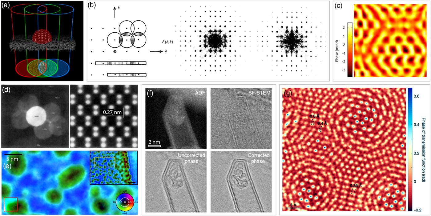
Fig. 8. Electron ptychography. a: Experimental geometry showing how overlapping probes (either converged or defocused) can be used to solve the exit wave phase. b: (Left) Schematic of convolution of square lattice with circular and rectangular probes with overlapping regions shaded, from Hoppe (Reference Hoppe1969a). Optical interference between diffraction of square lattice with circular hole when (center) aligned to lattice point, and (right) aligned to center of four lattice points, from Hoppe & Strube (Reference Hoppe and Strube1969). c: Ptychographic reconstruction of twisted bilayer graphene, from Pennycook et al. (Reference Pennycook, Lupini, Yang, Murfitt, Jones and Nellist2015). d: Reconstruction of periodic silicon lattice, from Nellist et al. (Reference Nellist, McCallum and Rodenburg1995). e: Atomic-resolution ptychographic imaging of aperiodic samples in a modified SEM, adapted from Humphry et al. (Reference Humphry, Kraus, Hurst, Maiden and Rodenburg2012), with contrast-enhanced inset. f: Simultaneous imaging modes including WDD ptychography of double-walled nanotube containing carbon nanostructures and iodine atoms, from Yang et al. (Reference Yang, Rutte, Jones, Simson, Sagawa, Ryll, Huth, Pennycook, Green and Soltau2016b). g: Ptychographic reconstruction of twisted bilayer MoS2 which resolves 0.4 Å Mo dumbbells, from Jiang et al. (Reference Jiang, Chen, Han, Deb, Gao, Xie, Purohit, Tate, Park and Gruner2018).
Over the next two decades, a few theoretical studies of ptychography were published including Hawkes (Reference Hawkes1982) and Konnert & D'Antonio (Reference Konnert and D'Antonio1986), and also some experimental scanning microdiffraction studies including Cowley (Reference Cowley1984) and Cowley & Ou (Reference Cowley and Ou1989). However, the first reconstruction method for ptychography similar to modern methods has not been published to date (Bates & Rodenburg, Reference Bates and Rodenburg1989). These authors later published a substantially improved reconstruction method in Rodenburg & Bates (Reference Rodenburg and Bates1992), the Wigner-distribution deconvolution (WDD) method which is still in use today for electron ptychography. Also suggested in that paper was the use of iterative methods for ptychography, examples of which were published in Faulkner & Rodenburg (Reference Faulkner and Rodenburg2004), Rodenburg & Faulkner (Reference Rodenburg and Faulkner2004), Maiden & Rodenburg (Reference Maiden and Rodenburg2009), and other studies. Another nonlinear approach to ptychographic reconstruction was proposed by D'alfonso et al. (Reference D'alfonso, Morgan, Yan, Wang, Sawada, Kirkland and Allen2014).
Early experimental demonstrations of the principles of ptychography were published by Rodenburg et al. (Reference Rodenburg, McCallum and Nellist1993), and the first experiment which imaged past the conventional TEM information limit using ptychography was published by Nellist et al. (Reference Nellist, McCallum and Rodenburg1995). This result, shown in Figure 8d, reconstructed the structure factors for a small number of diffraction vectors, a method which requires a periodic sample. Iterative ptychography in TEM experiments that used information contained inside the STEM probe BF disk was shown by Hüe et al. (Reference Hüe, Rodenburg, Maiden, Sweeney and Midgley2010), and shortly thereafter Putkunz et al. (Reference Putkunz, DAlfonso, Morgan, Weyland, Dwyer, Bourgeois, Etheridge, Roberts, Scholten and Nugent2012) demonstrated atomic-scale ptychography by imaging boron nanocones. In the same year, ptychographic reconstructions that used the electron intensity scattered beyond the probe-forming angular range were published by Humphry et al. (Reference Humphry, Kraus, Hurst, Maiden and Rodenburg2012), reproduced in Figure 8e.
Using 4D-STEM experiments and a non-iterative “single-side band” reconstruction method, atomic resolution ptychography reconstructions of bilayer graphene were shown by Pennycook et al. (Reference Pennycook, Lupini, Yang, Murfitt, Jones and Nellist2015), and are plotted in Figure 8c. This work was followed by a theoretical paper by Yang et al. (Reference Yang, Pennycook and Nellist2015b) which derived the optimum imaging conditions for focused probe ptychography and analyzed the advantages of using 4D-STEM over segmented detectors. This same group also used WDD ptychography and conventional imaging modes to analyze complex nanostructures in Yang et al. (Reference Yang, Rutte, Jones, Simson, Sagawa, Ryll, Huth, Pennycook, Green and Soltau2016b), shown in Figure 8f. To date, the highest resolution 4D-STEM ptychography experiments have been performed by Jiang et al. (Reference Jiang, Chen, Han, Deb, Gao, Xie, Purohit, Tate, Park and Gruner2018). These experiments imaged bilayer MoS2, plotted in Figure 8g. This paper estimated a resolution of 0.39 Å using an electron voltage of 80 kV, significantly beyond the conventional imaging resolution of 0.98 Å for these microscope parameters. Additionally, this paper also used simulations to determine that defocused-probe iterative ptychography outperformed both focused-probe iterative ptychography and the WDD reconstruction method by approximately a factor of 2 for signal-to-noise. Various authors have applied ptychography to solve materials science questions, including Yang et al. (Reference Yang, Jones, Ryll, Simson, Soltau, Kondo, Sagawa, Banba, MacLaren and Nellist2015a, Reference Yang, MacLaren, Jones, Martinez, Simson, Huth, Ryll, Soltau, Sagawa and Kondo2017), Wang et al. (Reference Wang, Zhang, Gao, Zhang and Kirkland2017), dos Reis et al. (Reference dos Reis, Yang, Ophus, Ercius, Bizarri, Perrodin, Shalapska, Bourret, Ciston and Dahmen2018), Lozano et al. (Reference Lozano, Martinez, Jin, Nellist and Bruce2018), and Fang et al. (Reference Fang, Wen, Allen, Ophus, Han, Kirkland, Kaxiras and Warner2019).
An interesting expansion of ptychography is the use of “hollow” diffraction patterns, whereby the 4D-STEM detector has a hole drilled in the center to allow for part or all of the unscattered electron beam to pass through into a spectrometer. Song et al. (Reference Song, Ding, Allen, Sawada, Zhang, Pan, Warner, Kirkland and Wang2018) showed that even with part of the measurement signal removed, atomic-resolution phase signals can still be reconstructed. This “hollow” detector configuration is compatible with a large number of 4D-STEM techniques discussed in this paper and we expect it to find widespread use once dedicated “hollow” pixelated STEM detectors are widely available.
Ptychography is a computational imaging method; thus in addition to benefiting from hardware such as aberration correction or better 4D-STEM detectors, algorithmic improvements are also possible. Some promising research avenues for electron ptychography have been explored in Thibault & Menzel (Reference Thibault and Menzel2013), Pelz et al. (Reference Pelz, Qiu, Bücker, Kassier and Miller2017), and other studies. Some authors have also explored expanding ptychography to a 3D technique by using a multislice method, including Gao et al. (Reference Gao, Wang, Zhang, Martinez, Nellist, Pan and Kirkland2017). Others are making use of the redundancy in 4D-STEM ptychographic measurements to apply ideas from the field of compressed sensing in order to reduce the number of required measurements, such as the study by Stevens et al. (Reference Stevens, Yang, Hao, Jones, Ophus, Nellist and Browning2018).
Phase Structured Electron Probes
Both DPC and ptychography rely on overlapping adjacent STEM probes to create enough redundant information for the phase of the object wave to be reconstructed. Alternatives to lateral-shift or COM DPC were also discussed in the work by Rose (Reference Rose1974). Rose derived that the ideal detector for measuring phase contrast from radially symmetric STEM probes is a difference signal between alternating radially symmetric “zones” aligned with the oscillations in the STEM probe's contrast transfer function, a concept further developed by Hammel & Rose (Reference Hammel and Rose1995). The combination of defocus and spherical aberration can produce a STEM probe with a known contrast transfer function which is divided into regions of approximately 0 and π/2 rad phase shift, as shown in Figure 9c. These alternating zones are matched to multiple annular detector rings, where the probe intensity incident onto each ring is measured independently. By measuring the difference signal between the 0 and π/2 zones, the local sample phase can be measured directly with a weighted detector such as that shown in Figure 9c. This method is essentially an extension of the ABF measurement method described above (Findlay et al., Reference Findlay, Shibata, Sawada, Okunishi, Kondo and Ikuhara2010). However, using the probe defocus and spherical aberration limits how many difference zones can be used, and using annular ring detectors requires very precise and stable alignment of the probe with respect to the detectors.
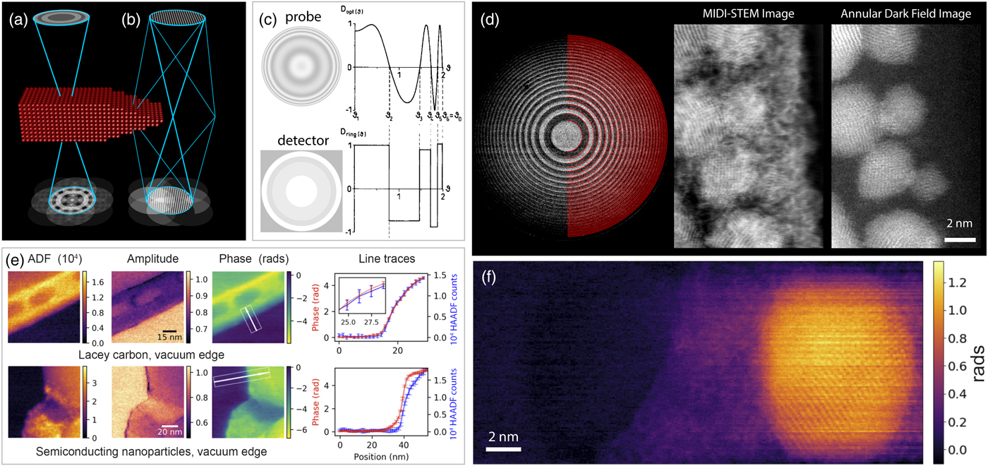
Fig. 9. 4D-STEM phase contrast measurements using structured phase probes. a: Schematic of MIDI-STEM and (b) STEMH experimental geometry. c: Initial MIDI-STEM proposal, adapted from Hammel & Rose (Reference Hammel and Rose1995). d: MIDI-STEM experiment including phase plate image and fitted virtual detector rings, output phase contrast MIDI-STEM image, and simultaneous HAADF image, adapted from Ophus et al. (Reference Ophus, Ciston, Pierce, Harvey, Chess, McMorran, Czarnik, Rose and Ercius2016). e: Experimental demonstration of STEMH, adapted from Harvey et al. (Reference Harvey, Yasin, Chess, Pierce, dos Reis, Özdöl, Ercius, Ciston, Feng, Kotov, McMorran and Ophus2018). f: Atomic resolution STEMH phase contrast reconstruction, adapted from Yasin et al. (Reference Yasin, Harvey, Chess, Pierce, Ophus, Ercius and McMorran2018c).
This phase contrast measurement technique was recently updated in two ways: first by using a phase plate to produce the desired probe illumination where 50% of the probe in reciprocal space is phase shifted by π/2 rad, while the remaining regions are not phase shifted (note the shape of these zones does not matter), an experimental geometry shown in Figure 9a. Second, a pixelated electron detector is used to measure the transmitted probes in diffraction space (i.e., a 4D-STEM measurement), where a virtual detector can then be exactly matched to the phase plate pattern. This method was termed “matched illumination and detector interferometry” (MIDI)-STEM, demonstrated experimentally at atomic resolution by Ophus et al. (Reference Ophus, Ciston, Pierce, Harvey, Chess, McMorran, Czarnik, Rose and Ercius2016), shown in Figure 9d. MIDI-STEM produces contrast with significantly less high-pass filtering than DPC or ptychography, but is less efficient at higher spatial frequencies. Interestingly, combining MIDI-STEM with ptychography produces additional contrast making it more efficient than either method used alone (Yang et al., Reference Yang, Ercius, Nellist and Ophus2016a). The use of MIDI-STEM for optical sectioning was recently investigated by Lee et al. (Reference Lee, Kaiser and Rose2019), who refer to this technique (without a material phase plate) as annular differential phase contrast.
Each of the previously discussed methods for phase contrast imaging in 4D-STEM applies high-pass filtering of the phase signal of the sample to some degree. This limits the ability to use these methods to quantitatively measure the phase shift of extended, low phase shift signals such as those induced by electric or magnetic fields (Haas et al., Reference Haas, Rouvière, Boureau, Berthier and Cooper2018). Recovering the low spatial frequencies can, however, be accomplished by using a reference wave, which could, for example, be generated by applying a potential to a biprism wire as in conventional electron holography (Möllenstedt & Düker, Reference Möllenstedt and Düker1956). The use of a biprism wire in STEM was first discussed by Cowley (Reference Cowley2003), but at the time detector technology was not sufficient to measure fringe shifts of a STEM-holography (STEMH) signal for many probe positions.
Another way to generate a reference wave is to use a diffraction grating in the probe-forming aperture to general multiple STEM probes, as in Figure 9b. This has been realized in 4D-STEM experiments by Harvey et al. (Reference Harvey, Yasin, Chess, Pierce, dos Reis, Özdöl, Ercius, Ciston, Feng, Kotov, McMorran and Ophus2018), shown in Figure 9e. By passing some of the STEM beams through vacuum and others through the sample and then measuring the fringe amplitudes and position, the absolute phase shift can be directly determined. Line traces of the experiments in Figure 9e show no phase shift in the vacuum for conductive lacey carbon, and a non-zero phase shift over vacuum outside of semiconducting nanoparticles, which was attributed to the electric field due to charging. Phase plate STEMH has also been demonstrated at atomic resolution by Yasin et al. (Reference Yasin, Harvey, Chess, Pierce, Ophus, Ercius and McMorran2018c), shown in Figure 9f. The STEMH method and some extensions are further discussed in Yasin et al. (Reference Yasin, Harada, Shindo, Shinada, McMorran and Tanigaki2018a, Reference Yasin, Harvey, Chess, Pierce and McMorran2018b).
Beyond 2D Projection and Kinematical Scattering
One of the weaknesses of electron scattering as opposed to X-ray or light scattering is that the strong interaction between electrons and matter leads to multiple scattering for all but the thinnest samples (Bethe, Reference Bethe1928). This “dynamical” scattering can be a problem when trying to quantitatively solve structures, but also presents an opportunity; it can be used to provide additional information about the sample along the beam direction. We previously mentioned the possible extension of ptychography to a 3D imaging method, discussed in Gao et al. (Reference Gao, Wang, Zhang, Martinez, Nellist, Pan and Kirkland2017). This is one possible route to going beyond the 2D projection assumption, and here we briefly discuss this approach and a few others that make use of 4D-STEM experimental data. A reconstruction from Gao et al. (Reference Gao, Wang, Zhang, Martinez, Nellist, Pan and Kirkland2017) is plotted in Figure 10a, which was calculated using the inverse multislice method for ptychography proposed by Maiden et al. (Reference Maiden, Humphry and Rodenburg2012). A non-iterative technique to recover 3D information is the “optical sectioning” method using WDD ptychographic reconstructions at different focal planes, which was shown in Yang et al. (Reference Yang, Rutte, Jones, Simson, Sagawa, Ryll, Huth, Pennycook, Green and Soltau2016b).
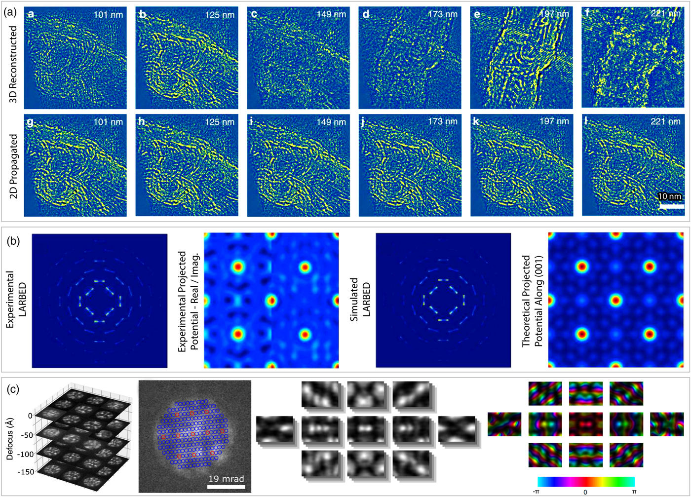
Fig. 10. 4D-STEM measurements beyond the projection assumption. a: Slices from 3D-ptychographic reconstruction of multiwalled carbon nanotubes, compared with Fresnel propagation of 2D reconstruction, from Gao et al. (Reference Gao, Wang, Zhang, Martinez, Nellist, Pan and Kirkland2017). b: LARBED measurement and reconstructed potential of SrTiO3, from Wang et al. (Reference Wang, Pennington and Koch2016). c: Focal series of 4D-STEM datasets used to recover scattering matrix for (110) Si, from Brown et al. (Reference Brown, Chen, Weyland, Ophus, Ciston, Allen and Findlay2018).
A 4D-STEM method which solves for structure factors in the presence of dynamical scattering was shown by Wang et al. (Reference Wang, Pennington and Koch2016). The experimental protocol used was varying the STEM probe tilt as opposed to position. By changing the relative amount of beam tilt above and below the sample (beam scan and descan respectively), this large-angle rocking-beam electron diffraction (LARBED) method developed by Koch (Reference Koch2011) can dramatically increase the maximum scattering angle present in each diffraction disk, relative to conventional CBED. An experimental reconstruction published by Wang et al. (Reference Wang, Pennington and Koch2016) is shown in Figure 10b, where the large scattering vectors in LARBED allow inversion of the structure factors for SrTiO3.
Another method to solve for the projected potential of thick crystals with substantial dynamical scattering is based on the idea that if the complex scattering matrix can be measured, it can be directly inverted into the structure matrix, as shown by Spence (Reference Spence1998) and Allen et al. (Reference Allen, Faulkner and Leeb2000). This concept has been employed by Brown et al. (Reference Brown, Chen, Weyland, Ophus, Ciston, Allen and Findlay2018), who used a series of 4D-STEM measurements at different probe defocus values to measure the scattering matrix for crystalline silicon, plotted in Figure 10c. From this scattering matrix, they were able to directly invert the structure matrix, a result they compared with DPC measurements using both experiment and simulation.
Real-space 4D-STEM
In the final experimental section of this paper, we review some interesting experiments that further extend the capabilities of 4D-STEM by imaging the electron distribution in real space, i.e., in a plane conjugate to the sample plane as shown in Figure 11a. In this confocal configuration, apertures placed just above the detector plane can select a range of incoming ray angles, leading to enhanced depth and energy resolution. This imaging mode has long been used in optical microscopy (Webb, Reference Webb1996), and was extended to electron microscopy first by Frigo et al. (Reference Frigo, Levine and Zaluzec2002) who dubbed the method scanning confocal electron microscopy (SCEM). Nellist et al. (Reference Nellist, Behan, Kirkland and Hetherington2006) introduced the use of two aberration corrections in order to extend SCEM to atomic resolution, using the experimental geometry shown in Figure 11b. The first corrector is used to form an atomic-scale probe pre-specimen to remove the aberrations of the first objective lens, while the second corrector is applied post-specimen to remove the aberrations of the second objective lens. Nellist et al. (Reference Nellist, Behan, Kirkland and Hetherington2006) were able to directly image the electron probe wavefunction at atomic resolution, improving on the resolution of previous similar measurements by Möbus & Nufer (Reference Möbus and Nufer2003).
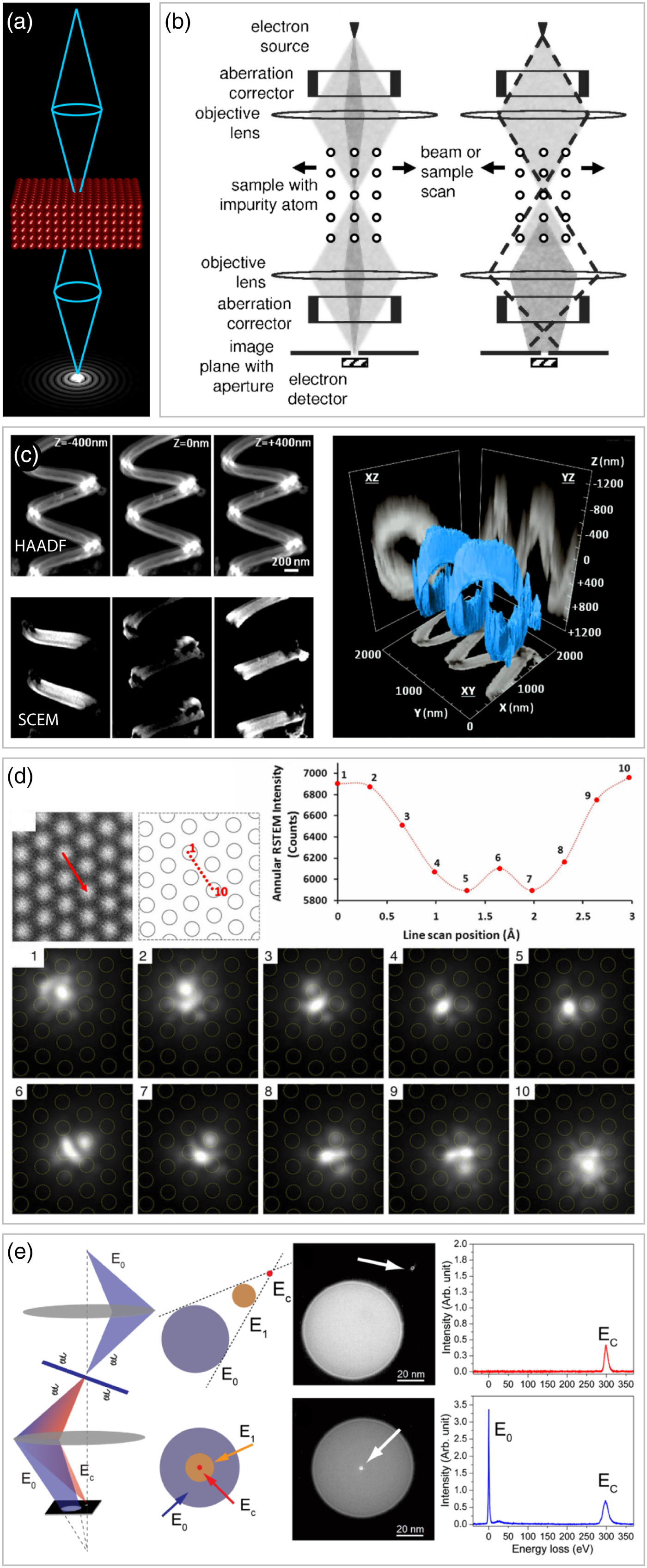
Fig. 11. R-STEM/SCEM. a: Schematic of imaging condition where detector plane is conjugated to the sample plane. b: Diagram showing how dual aberration corrections for reciprocal and real space can be used to implement SCEM, from Nellist et al. (Reference Nellist, Behan, Kirkland and Hetherington2006). c: 3D reconstruction of carbon nanocoils using SCEM, adapted from Hashimoto et al. (Reference Hashimoto, Shimojo, Mitsuishi and Takeguchi2009). d: Double aberration-corrected images of electron probe in real-space after passing through crystallizing gold, from Etheridge et al. (Reference Etheridge, Lazar, Dwyer and Botton2011). e: Diagram showing how off-axis SCEM can be used to measure inelastic scattering, experimental comparison of on- and off-axis SCEM imaging of carbon with 300 eV edge, compared with EELS measurements of the same edge, adapted from Zheng et al. (Reference Zheng, Zhu, Lazar and Etheridge2014).
One of the most powerful potential uses of SCEM is 3D imaging without needing to tilt the sample. Zaluzec (Reference Zaluzec2007) demonstrated both improved resolution of SCEM over TEM and 3D imaging using the reduced depth of the field of SCEM. Figure 11c shows a comparison between defocused images of carbon nanocoils taken with conventional HAADF imaging compared with a SCEM measurement by Hashimoto et al. (Reference Hashimoto, Shimojo, Mitsuishi and Takeguchi2009). SCEM significantly improved the depth resolution, allowing Hashimoto et al. (Reference Hashimoto, Shimojo, Mitsuishi and Takeguchi2009) to reconstruct the 3D helical nanocoil, also plotted in Figure 11c. SCEM depth-sectioning measurements can also be performed using 4D-STEM. Hamaoka et al. (Reference Hamaoka, Hashimoto, Mitsuishi and Takeguchi2018) demonstrated that by using an annular aperture below the specimen and recording the full diffraction pattern, 3D information from the sample could be obtained using virtual ring detectors.
By adding scanning to the experiments performed by Nellist et al. (Reference Nellist, Behan, Kirkland and Hetherington2006) and Etheridge et al. (Reference Etheridge, Lazar, Dwyer and Botton2011) were able to perform “4D-SCEM” experiments to directly measure the electron probe wavefunction intensity after scattering from a gold crystal. These experiments which the authors refer to as “realspace scanning transmission electron microscopy” (R-STEM) are reproduced in Figure 11d, where the electron probe was moved between two atomic columns. As the probe traverses the sample, the intensity distribution is strongly modulated by scattering from the sample, due to dynamical and channeling effects. This direct measurement of the electron distribution within the sample was previously only available via simulation. This has important ramifications for inelastic scattering measurements with electron spectroscopy, which the authors demonstrate with measurements of the probe after scattering from a plasmon. The same group also demonstrated direct measurements of chromatic aberration coefficients in STEM in Zheng & Etheridge (Reference Zheng and Etheridge2013). Another follow-up paper by Zheng et al. (Reference Zheng, Zhu, Lazar and Etheridge2014) introduced the concept of “off-axis” SCEM, which is shown in Figure 11e. By tilting the incident STEM probe and varying the post-scattering defocus, they use the chromatic aberration of the system in order to create a 3D dispersion which allows for spectroscopic measurements of the STEM probe without a spectrometer (i.e., without energy dispersive electron optics). Figure 11e also shows the verification of these off-axis SCEM measurements using conventional STEM-EELS spectroscopy. Further information on R-STEM experiments can be found in studies by Lazar et al. (Reference Lazar, Etheridge, Dwyer, Freitag and Botton2011) and Dwyer et al. (Reference Dwyer, Lazar, Chang and Etheridge2012).
4D-STEM Simulation Methods
Finally, we want to briefly mention the role of simulations in 4D-STEM studies. Previously discussed examples such as Liu et al. (Reference Liu, Neish, Stokol, Buckley, Smillie, de Jonge, Ott, Kramer and Bourgeois2013), Ophus et al. (Reference Ophus, Ercius, Sarahan, Czarnik and Ciston2014), Yang et al. (Reference Yang, Pennycook and Nellist2015b, Reference Yang, MacLaren, Jones, Martinez, Simson, Huth, Ryll, Soltau, Sagawa and Kondo2017); Bruma et al. (Reference Bruma, Santiago, Alducin, Plascencia Villa, Whetten, Ponce, Mariscal and José-Yacamán2016), Xu & LeBeau (Reference Xu and LeBeau2018), and many others relied heavily on simulation to interpret the 4D-STEM results, not to mention the many ideas which are initially tested on, or verified by, simulations. TEM simulations are typically performed with one of two algorithms: Bloch wave scattering matrix (S-matrix) calculations (Bethe, Reference Bethe1928; Humphreys, Reference Humphreys1979), or the multislice method (Cowley & Moodie, Reference Cowley and Moodie1957; Goodman & Moodie, Reference Goodman and Moodie1974). STEM simulations typically require significantly more calculations than plane-wave TEM calculations, since the scattering of each probe is different. In addition to this, 4D-STEM simulations require storing the full 4D output signal which could potentially require a large amount of disk storage space (Ophus et al., Reference Ophus, Yang, dos Reis, Meng, Pryor, Miao, Pekin, Minor, Johnson and Denes2017b). Therefore, large 4D-STEM simulation studies usually employ the multislice method (which scales more efficiently with system size than Bloch wave methods) and utilize parallelization either over multiple central processing units, or use one or more graphics processing units. Ophus (Reference Ophus2017) has recently developed a hybrid S-matrix and multislice simulation method that can potentially provide a large speed up for 4D-STEM simulations. Some codes that can perform 4D-STEM simulations “out of the box” include μSTEM (Forbes et al., Reference Forbes, Martin, Findlay, DAlfonso and Allen2010), Prismatic (Pryor et al., Reference Pryor, Ophus and Miao2017), STEMsalabim (Oelerich et al., Reference Oelerich, Duschek, Belz, Beyer, Baranovskii and Volz2017), and Dr. Probe (Barthel, Reference Barthel2018).
Conclusion
This review has covered a broad cross-section of 4D-STEM experimental methods. We have chosen to focus on the wide breadth of measurements possible with 4D-STEM, as opposed to going into depth on a few topics. We hope that this review will give materials scientists ideas for new measurements they can apply to their samples using 4D-STEM, and that it provides the key references required to learn more about each of these measurement techniques. 4D-STEM methods will likely see widespread deployment, due to the current fast pace of detector hardware development, and increasing availability of analysis software. Eventually, these methods will become available and accessible enough that 4D-STEM will become just STEM.
Author ORCIDs
Colin Ophus, 0000-0003-2348-8558.
Acknowledgments
We wish to thank Holly Barton, Thomas Pekin, Steven Zeltmann, Benjamin Savitzky, Hamish Brown, and Karen Bustillo for helpful suggestions and proof-reading of this paper. We thank Roberto dos Reis, Jim Ciston, and Peter Ercius for providing 4D-STEM datasets. We also thank Alexander Mueller for helpful translations of German manuscripts, and David Muller for suggesting the title of this manuscript. CO acknowledges support from the US Department of Energy Early Career Research Program. Work at the Molecular Foundry was supported by the Office of Science, Office of Basic Energy Sciences, the US Department of Energy under Contract No. DE-AC02-05CH11231.


 Open access