


Introduction
The demonstration of robust room temperature ferroelectric and multiferroic properties that persist at sub-10 nm dimensions is crucial to their implementation in technologically competitive data storage applications (Spaldin & Ramesh, Reference Spaldin and Ramesh2019). For instance, in purely electronic memristors where ultra-thin (<10 nm) ferroelectrics function as tunnel junctions, the junction resistance sensitively depends on the relative fraction of ferroelectric domains with polarization pointing toward one or the other electrode. Large (ca. 1,000:1) ON/OFF tunneling current ratios between resistance states can be achieved with nondestructive read operations (Luo et al., Reference Luo, Apachitei, Yang, Peters, Sanchez and Alexe2018). Additionally, because ferroelectric switching involves domain nucleation and growth, neuronal synaptic learning mechanisms can be mimicked (Boyn et al., Reference Boyn, Grollier, Lecerf, Xu, Locatelli, Fusil, Girod, Carrétéro, Garcia, Xavier, Tomas, Bellaiche, Bibes, Barthélémy, Saïghi and Garcia2017). Fine-tuning of conductance enables artificial nano-synapses to be created, where synaptic strengths evolve depending on the switching pulse amplitude and duration. Although not yet realized in practice, due to the rarity of suitable materials and current limitations in material properties (Spaldin & Ramesh, Reference Spaldin and Ramesh2019), storage devices based on ultra-thin multiferroic tunnel junctions (possessing simultaneous ferroelectric and ferromagnetic memory states) would offer an attractive opportunity for combining electroresistance states with magnetoresistance states (Yang et al., Reference Yang, Tang, Ye, Zhou, Zheng, Tang, Zhang and He2007). This would provide the capability to produce four or more different logic states. Within each state, multiple levels of resistance could be created by controlling domain evolution, and thus offers tantalizing prospects for unique, multi-state, multi-level memory elements in future neuromorphic (“brain-inspired”) computing systems (Baudry et al., Reference Baudry, Lukyanchuk and Vinokur2017).
A challenge to the commercialization of devices based on out-of-plane tunnel junctions is the formation of polarization-induced surface charges induced by the out-of-plane polarization which can produce a depolarization field of magnitude inversely proportional to the dimensions of the ferroelectric (Denev et al., Reference Denev, Lummen, Barnes, Kumar and Gopalan2011). This means that below a critical thickness, out-of-plane ferroelectricity will be suppressed, leading to a lack of stability and reproducibility in vertical tunnel junctions at reduced dimensions. Alternatively, devices based on in-plane tunnel junctions would not be hindered by competing depolarization fields upon scaling down to ultra-thin dimensions, meaning that higher ON:OFF tunneling current ratios can be achieved with nondestructive read operations. So far, device concepts based on theoretical simulations of monochalcogenides have been proposed (Chang et al., Reference Chang, Liu, Lin, Wang, Zhao, Zhang, Jin, Zhong, Hu, Duan, Zhang, Fu, Xue, Chen and Ji2016; Liu et al., Reference Liu, Chang, JI, Chen and Fu2018; Shen et al., Reference Shen, Liu, Chang and Fu2019a, Reference Shen, Fang, Tian and Duan2019b); however, such an in-plane device is yet to be validated for ultra-thin ferroelectrics that can be synthesized by scalable growth methods.
Layered structured materials, such as the bismuth-based Aurivillius phases [general formula (Bi2O2)(Am−1BmO3m+1)] offer very flexible frameworks for a wide variety of applications, given that differing cations can be accommodated both at the A- and B-sites. Aurivillius phases (Fig. 1a) (Ismunandar et al., Reference Ismunandar, Hoshikawa, Zhou, Kennedy, Kubota and Kato2004; Momma & Izumi, Reference Momma and Izumi2011) are naturally 2D (two dimensional) nanostructured, where (Bi2O2)2+ fluorite-type layers are interleaved with m numbers of perovskite-type units. Indeed, in-plane ferroelectricity at Curie temperatures above 650°C has been established in Aurivillius 100 nm thin films by several industrially scalable growth methods (Deepak et al., Reference Deepak, Zhang, Keeney, Pemble and Whatmore2013; Faraz et al., Reference Faraz, Deepak, Schmidt, Pemble and Keeney2015, Reference Faraz, Maity, Schmidt, Deepak, Roy, Pemble, Whatmore and Keeney2017). Furthermore, the manganese-containing m = 5 Aurivillius phase Bi6TixFeyMnzO18 system is a rare example of a single-phase room temperature multiferroic. Previous studies have shown that when B-site Ti (x) is maintained between 2.80 and 3.04, Fe (y) between 1.32 and 1.52, and Mn (z) between 0.54 and 0.64, thin film samples on sapphire display saturation magnetization (M S) values as high as 215 emu/cm3 and in-plane saturation polarization (P s) values of >26 μC/cm2, and demonstrate magnetoelectric switching at room temperature (Keeney et al., Reference Keeney, Maity, Schmidt, Amann, Deepak, Petkov, Roy, Pemble and Whatmore2013, Reference Keeney, Downing, Schmidt, Pemble, Nicolosi and Whatmore2017, Reference Keeney, Saghi, O'Sullivan, Alaria, Schmidt and Colfer2020b; Schmidt et al., Reference Schmidt, Amann, Keeney, Pemble, Holmes, Petkov and Whatmore2014; Faraz et al., Reference Faraz, Maity, Schmidt, Deepak, Roy, Pemble, Whatmore and Keeney2017).
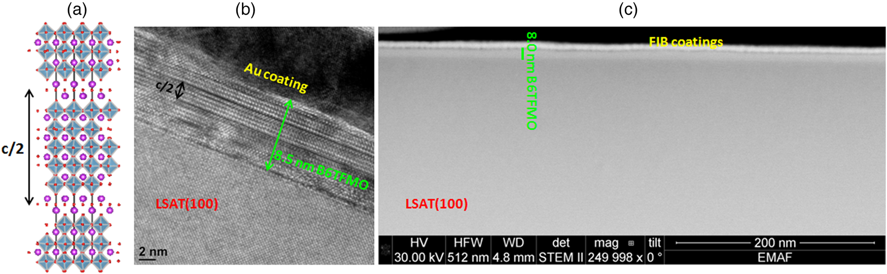
Fig. 1. (a) Schematic of a B2eb (Ismunandar et al., Reference Ismunandar, Hoshikawa, Zhou, Kennedy, Kubota and Kato2004) m = 5 Aurivillius phase crystal structure projected down the <110> orientation produced using VESTA (Momma & Izumi, Reference Momma and Izumi2011) software. Bismuth atoms are represented by purple spheres, oxygen atoms are represented by smaller red spheres, and BO6 octahedra are represented by blue polyhedra. Half a unit cell (c/2) of the structure is comprised of five perovskite blocks interleaved between fluorite-type bismuth oxide layers. (b) Representative TEM image of B6TFMO on LSAT (100) where 5% excess bismuth precursor was utilized during the 700°C DLI-CVD process. (c) Representative STEM image of B6TFMO on LSAT (100) where 49% excess bismuth precursor was utilized during the 700°C DLI-CVD process.
As Figure 1a shows, a unit cell of the Aurivillius phase structure along “c” is comprised of two sets of m perovskite ABO3 blocks divided by a fluorite (Bi2O2)+ layer. Thus, with the potential to cleave the structure at the fluorite layers, Aurivillius phase materials are amenable starting materials for exfoliation into 2D nano-sheets. Recently, we have shown that ferroelectricity can persist in m = 4 exfoliated Aurivillius phase nano-flakes produced by an ultrasonic exfoliation method with thicknesses of only 2.4 nm (Keeney et al., Reference Keeney, Smith, Palizdar, Schmidt, Bell, Coleman and Whatmore2020a). This equates to one-half of the normal crystal unit cell (or in the case of m = 4, four perovskite oxide blocks plus the associated Bi2O2 layers, c/2; Fig. 1a), demonstrating that Aurivillius phase wide-bandgap oxide ferroelectrics can be added to the growing class of 2D materials.
In order to increase the technological potential of Bi6TixFeyMnzO18 for utilization in future devices, an industrially scalable direct liquid injection chemical vapor deposition (DLI-CVD) process was subsequently developed (Keeney et al., Reference Keeney, Saghi, O'Sullivan, Alaria, Schmidt and Colfer2020b) for the synthesis of epitaxial ferroelectric m = 5 Bi6Ti2.9Fe1.5Mn0.6O18 (B6TFMO) films of sub-10 nm thickness. The nominal Bi6Ti2.9Fe1.5Mn0.6O18 composition was chosen to allow for insertion of larger magnetic cations (atomic radii of between 0.645 and 0.82 Å) (Shannon, Reference Shannon1976; Keeney et al., Reference Keeney, Downing, Schmidt, Pemble, Nicolosi and Whatmore2017), while preserving a 58% composition of the smaller Ti4+ cation (0.605 Å) (Shannon, Reference Shannon1976; Keeney et al., Reference Keeney, Downing, Schmidt, Pemble, Nicolosi and Whatmore2017) at the B-site so that the m = 5 Aurivillius structure is maintained. Unfortunately, epitaxial growth of this complex oxide is confounded by the volatility of the bismuth oxide species, which can result in microstructural defects and the formation of magnetic impurities (Alexe et al., Reference Alexe, Scott, Curran, Zakharov, Hesse and Pignolet1998). An excess of 5–8% for the bismuth precursor, at a deposition temperature of 700°C, was employed to attempt to compensate for bismuth volatility and to sustain a Bi6 stoichiometry. However, using this modest bismuth excess, a volume fraction of ferrimagnetic spinel (Mn, Fe)3O4 impurities at the film surface was observed at the order of 3–4 vol%, as identified by a combination of atomic force microscopy (AFM) and transmission electron microscopy (TEM) (Keeney et al., Reference Keeney, Saghi, O'Sullivan, Alaria, Schmidt and Colfer2020b). While these types of impurities are not ferroelectric and would not contribute to a ferroelectric signal; impurities and microstructural defects are known to influence domain wall activity in ferroelectric thin films and may contribute to “pinning effects” which can have resistance to domain wall motion (Luborsky et al., Reference Luborsky, Livingston, Chin, Cahn and Haasen1996). Although possible domain wall pinning by defects and impurities did not prevent local switching of lateral ferroelectric domains in B6TFMO synthesized with an excess of 5% bismuth precursor (Keeney et al., Reference Keeney, Saghi, O'Sullivan, Alaria, Schmidt and Colfer2020b), microstructural resistance to domain-wall motion may be an issue for macroscopic ferroelectric switching. Therefore, secondary phase impurities should be minimized in order to improve ferroelectric switching behavior. Importantly, we have learned from prior work (Keeney et al., Reference Keeney, Kulkarni, Deepak, Schmidt, Petkov, Zhang, Cavill, Roy, Pemble and Whatmore2012; Schmidt et al., Reference Schmidt, Amann, Keeney, Pemble, Holmes, Petkov and Whatmore2014; Faraz et al., Reference Faraz, Ricote, Jimenez, Maity, Schmidt, Deepak, Roy, Pemble and Keeney2018) that even trace (~0.01 vol%) amounts of impurities present in a sample can be responsible for an observed magnetic response in the bulk material. The elimination of possible magnetic impurity phases and rigorous analysis of sample purity, together with statistical analysis, is required in order to conclude with confidence that impurities are not affecting the magnetic measurements observed (Schmidt et al., Reference Schmidt, Amann, Keeney, Pemble, Holmes, Petkov and Whatmore2014). Without such, one cannot be confident that a sample is truly a single-phase multiferroic and thus limits its use. The investigation of ferromagnetic properties was thus precluded in our 2020 work (Keeney et al., Reference Keeney, Saghi, O'Sullivan, Alaria, Schmidt and Colfer2020b), given that the magnetic impurities would complicate attempts to measure ferromagnetic signal intrinsic to the main B6TFMO Aurivillius phase.
In order to counteract the volatility of the bismuth oxide species during growth and to sustain a Bi6 stoichiometry, the focus of this contribution is to explore the use of relatively large bismuth excesses to minimize the formation of magnetic spinel impurity phases. In previous work by Deepak et al. (Reference Deepak, Zhang, Keeney, Pemble and Whatmore2013, Reference Deepak, Carolan, Keeney, Zhang, Pemble and Whatmore2015a, Reference Deepak, Carolan, Keeney, Pemble and Whatmore2015b), a bismuth self-limiting process was developed for the synthesis of epitaxial bismuth-based ferroelectric thin films by DLI-CVD. This enabled an extension of the DLI-CVD growth window and the use of bismuth precursor excesses of between 33 and 81%, without leading to the formation of impurity phases. Based on this, bismuth precursor excess of 49% was utilized in this work, and AFM investigations demonstrated that this considerably decreased impurity concentrations (as much as 200-fold), compared with samples grown using only a 5% bismuth precursor excess.
Ferroelectric measurements of sub-10 nm films can be experimentally challenging. Whereas polarization versus electric-field (P–E) measurements enabled measurements of ferroelectric switching in previously grown 100 nm thick samples (in-plane P s > 26 μC/cm2) (Faraz et al., Reference Faraz, Ricote, Jimenez, Maity, Schmidt, Deepak, Roy, Pemble and Keeney2018), these measurements are often made difficult by leakage currents when the thickness decreases below a few tens of nanometers. Indications of a polar state may be deduced from diffraction studies, but to demonstrate the existence of a switchable polarization at nano-scale, piezoresponse force microscopy (PFM) is the technique of preference (Garcia et al., Reference Garcia, Fusil, Bouzehouane, Enouz-Vedrenne, Mathur, Barthélémy and Bibes2009). There has been considerable progress in PFM instrumentation over the last two decades, and this technique was employed in this study to investigate the ferroelectric properties of the sub-10 nm B6TFMO samples. PFM experiments demonstrate that stable ferroelectric domains persist in ~8 nm B6TFMO films, with an isotropic random distribution of stable in-plane domains and out-of-plane domains having lower piezoresponse, consistent with expectations from crystal symmetry. The persistence of stable and switchable ferroelectricity at sub-10 nm thickness in B6TFMO, both in-plane and out-of-plane, initiates possibilities for miniaturizing novel multiferroic-based devices based on ultra-thin tunnel junctions. By developing an industrially scalable DLI-CVD method that reduces the volume fraction of magnetic impurities up to 200-fold in 8 nm B6TFMO films, this work demonstrates the recent advancements in the optimization of ultra-thin B6TFMO for future technologies incorporating single-phase multiferroic materials.
Materials and Methods
Thin Film Deposition
Aurivillius phase films with a nominal composition, Bi6Ti2.9Fe1.5Mn0.6O18 (B6TFMO), were prepared with a horizontal flow AIXTRON AIX 200/4FE AVD (atomic vapor deposition or direct liquid injection chemical vapor deposition (DLI-CVD)) system. Bismuth, iron, and titanium precursor solutions were commercially available from Epivalence Ltd. These were 0.1 mol/dm3 solutions of Bi(thd)3, Fe(thd)3, and Ti(O-iPr)2(thd)2 (where thd = 2,2,6,6-tetramethyl 3,5-heptanedione; O-iPr = isopropoxide) in toluene and were maintained under N2(g) (nitrogen gas) in stainless steel bubbler vessels. Mn(thd)3 (99%, STREM chemicals) was dissolved in anhydrous toluene (99.8%, Sigma-Aldrich) under N2(g) into a stainless steel bubbler vessel to a concentration of 0.025 mol/dm3 and used as manganese precursor. The pressure of the growth chamber was kept at 9 mbar. The growth chamber was a typical cold wall reactor with a susceptor heated substrate holder maintained at 700°C by means of an infrared lamp assembly. The liquid precursors were injected individually with the aid of inert N2(g) carrier gas into a vaporizer maintained at 220°C, using four individual injectors, one for each precursor source. The injected precursor volume (in the micro-liter range) was controlled by pulsing 100 injections for each precursor, and by setting the opening time of the injector (between 1.6 and 12.2 ms, depending on the precursor) for each pulse during a continuous injection mode at a frequency of 1 Hz. The amount of precursor injected was monitored with a liquid flow meter. The net volumetric precursor injection ratios for the B-site precursors were approximately 2.9:1.5:0.6 for Ti(O-iPr)2(thd)2:Fe(thd)3:Mn(thd)3, respectively, in order to yield B6TFMO with a nominal composition of Bi6Ti2.9Fe1.5Mn0.6O18. In order to investigate the influence of varied bismuth excess on film crystallinity and purity, bismuth precursor excesses of 5 and 49% were employed. The evaporated precursors were then transported through lines maintained at 220°C into a showerhead and mixed with reactive gas [O2(g) (oxygen gas)] to allow deposition on to the heated substrates. The total N2(g)/O2(g) flow in the growth chamber was 3,000 sccm, of which O2(g) flow was 1,000 sccm. The substrates used in this study were (100) oriented STO (SrTiO3) and LSAT (La0.26Sr0.76Al0.61Ta0.37O3) with average dimensions of 10 × 10 × 0.5 mm. The substrates were cleaned with isopropyl alcohol followed by distilled water and dried using N2(g). They were then rotated with 60 sccm N2(g) flow through a susceptor holder to permit improved uniformity.
Physical Characterization
The crystalline properties of the films were characterized using a Panalytical MRD X-ray diffraction (XRD) system with filtered Cu Kα radiation source (45 kV and 40 mA) over the range 5° ≤ 2θ ≤ 50°. Microstructural analysis by high-resolution TEM (HR-TEM) was conducted on a JEOL 2100 TEM, at 200 kV. Thickness analysis of the samples was performed by dark-field imaging using the scanning transmission electron microscopy (STEM) mode (FEI Helios Nanolab, Eindhoven, The Netherlands). To enable the HR-TEM and dark-field STEM imaging, the samples were gold-coated to prevent charging, followed by platinum coatings to facilitate FIB cross-sectioning. Cross-sections were prepared using an FEI Helios Nanolab 600i DualBeam focused ion beam-scanning electron microscope (FIB-SEM) (final thinning conditions: 93 pA current at 30 kV, final polish conditions: 47 pA current at 5 kV). A commercial atomic force microscope (AFM), Bruker Dimension Icon in PeakForce Tapping mode (with Bruker SCANASYST-AIR probes, Al reflex coated, 2 nm tip radius, 70 kHz resonant frequency), was used for topography mapping of the films. Measurements of film surface roughness and the analysis of surface impurity volume fraction were conducted by performing AFM measurements (1 μm × 1 μm scan area) over five different areas of the sample surface. Average root-mean-square (RMS) roughness (nm) values are presented along with the standard deviation (SD) variability of the dataset. Average volume fraction (vol%) values were calculated from the impurity particle count area as a proportion of the scan area and are presented along with the SD variability of the dataset.
Nano-Scale Ferroelectric Measurements
Electromechanical responses of the films were measured by PFM (piezoresponse force microscopy) using an Asylum Research MFP-3DTM AFM in contact mode equipped with an HVA220 amplifier for PFM and a cantilever scan angle of 90°. The single frequency mode (drive frequency = 15 kHz) enabled measurements of lateral and vertical piezoresponses, where the inverse optical lever sensitivity of the cantilevers was calibrated according to the MFP-3D Procedural Operation “Manualette,” the system inherent background was determined using a non-piezoelectric silicon wafer, and the PFM signal was then calibrated using α-quartz as a reference sample. The dual AC (alternating current) resonance tracking PFM (DART-PFM) mode was used to boost both the vertical and lateral piezo signals. In this mode, the PFM signal is measured at the tip-sample contact resonance frequency, with a higher signal-to-noise ratio compared with other frequencies. Topographical cross-talk is reduced using an amplitude feedback loop which tracks the contact resonance frequency so that drive frequencies are adjusted accordingly as the probe scans over the changing sample topography. The application of an AC bias to a conductive tip during contact mode imaging (V tip = V ACcos(ωt)) results in surface displacement (d) and deflection of cantilever due to the converse piezoelectric effect, with both normal and in-plane components. Piezoresponse is defined in the vertical/normal direction, ΔZ, as ±dzzV ACcos(ωt + θ) and in the lateral/in-plane directions, ΔL1 = ±dzxV ACcos(ωt + θ) and ΔL2 = ±dzyV ACcos(ωt + θ), where ω = angular frequency; t = time; θ = phase (0 or 180°). The definition for piezoresponse can be manipulated to Acosθ, which allows us to visualize the magnitude of the piezoresponse through the PFM amplitude (A) images and the direction of the polarization via the PFM phase (θ) images (Hong et al., Reference Hong, Woo, Shin, Jeon, Pak, Colla, Setter, Kim and No2001). Apex Super Sharp conductive diamond probes AD-2.8-SS (Au reflex coated, <5 nm tip radius, 75 kHz resonant frequency, boron-doped) were used to image piezoelectric domains over 1 μm × 1 μm scan areas and to investigate possible in-plane anisotropy (Figs. 4, 5). To investigate if the observed vertical piezoresponse truly arises from the out-of-plane polarization component of the film under investigation and not as a result of buckling of the cantilever, vertical PFM (Vert PFM) experiments were performed with the cantilever aligned parallel to the [010] substrate direction immediately followed by Vert PFM experiments after rotation of the sample by 90° so that the cantilever was aligned parallel to the [100] substrate direction. A similar Vert PFM signal and domain distribution for both sample directions confirms that a genuine out-of-plane piezoresponse from the sample is recorded during these Vert PFM experiments (Kalinin et al., Reference Kalinin, Rodriguez, Jesse, Shin, Baddorf, Gupta, Jain, Williams and Gruverman2006). The angular torsion of the cantilever as it oscillates was monitored in lateral PFM (Lat PFM) measurements, which were conducted in a similar manner to the Vert PFM measurements except the “InFast” option was programed to “Lateral” as opposed to “AC deflection,” and the drive frequencies were operated near contact resonance for lateral (670–720 kHz) and vertical (250–280 kHz) modes, respectively. Because the DART-PFM technique is designed to boost the piezo signal-to-noise ratio and minimize topographical “cross-talk,” it enabled probing AC drive amplitudes (V AC) of 2.0 V AC and below (typically 1.0 V AC in this work). The use of minimum as possible V AC is critical for ultra-thin films, where increased biases can result in dielectric breakdown and physical degradation of the surface of nanoscale structures (Rodriguez et al., Reference Rodriguez, Jesse, Alexe and Kalinin2008). Imaging of the same sample area by Vert PFM and Lat PFM allows complementary mapping of the normal component of the piezoresponse vector (out-of-plane direction) and the transversal component of the in-plane piezoresponse (perpendicular to the cantilever axis), respectively (Kalinin et al., Reference Kalinin, Rodriguez, Jesse, Shin, Baddorf, Gupta, Jain, Williams and Gruverman2006). There are no microscopic topographic markers on the surface and the same location cannot be found after physical sample rotation by 90°, thus preventing 3D-PFM imaging (Vert PFM and x, y-Lat PFM) and determination of the individual elements of the piezoelectric tensor. Ferroelectric lithography was performed over a larger scan area (5 μm × 5 μm; Fig. 6) using conductive Olympus AC240TM Electrilevers, Ti/Pt-coated silicon probes (Al reflex coated, 15 nm tip radius, 70 kHz resonant frequency). The Asylum Research PFM Lithography mode was performed by converting an imported grayscale image into a bias map and employing direct current (DC) voltages of ±7.0 V. The “write step” and Vert PFM imaging were performed with InFast set to “AC deflection,” and Lat PFM imaging was performed with InFast set to “Lateral.” The read step was performed with a probing signal of 2.0 V AC.
Results and Discussion
Investigating the Influence of Excess Bismuth Precursor on Sample Crystallinity and Purity
Thin films were synthesized by maintaining the titanium, iron, and manganese flows relatively constant and by varying the bismuth precursor flow between deposition runs so that bismuth excesses of between 5 and 49% were obtained. Given that the pseudo-lattice parameter of the perovskite-type layer ( $a_p^{\prime}$) in B6TFMO is 3.89 Å (Keeney et al., Reference Keeney, Saghi, O'Sullivan, Alaria, Schmidt and Colfer2020b), substrates with similar lattice constants to B6TFMO were chosen for the growth experiments. These were, namely, STO (100) (a = 3.905 Å; lattice mismatch = +0.39%) and LSAT (100) (a = 3.868 Å; lattice mismatch = −0.57%) substrates. HR-TEM (Fig. 1b) and dark-field STEM imaging (Fig. 1c) demonstrate that continuous ultra-thin films, ~8 nm in thickness, were successfully deposited on LSAT (100) and STO (100) substrates by the DLI-CVD process.
Figure 2 displays the XRD profiles of the B6TFMO films obtained under varied quantities (5 and 49%) of bismuth precursor excess on LSAT (100) (Fig. 2a) and STO (100) (Fig. 2b) substrates. Note that intensity is plotted in the logarithmic scale to emphasize weaker peaks. Five-layered B6TFMO Aurivillius phases were successfully achieved, as referenced against the m = 5 B2eb space group (Ismunandar et al., Reference Ismunandar, Hoshikawa, Zhou, Kennedy, Kubota and Kato2004). Notwithstanding, small regions with intergrowths of differing m phases (e.g., m = 4, m = 5, m = 6) are common in layered Aurivillius phases with relatively high structural anisotropy (Zurbuchen et al., Reference Zurbuchen, Tian, Pan, Fong, Streiffer, Hawley, Lettieri, Jia, Asayama, Fulk, Comstock, Knapp, Carim and Schlom2007). This local disorder, along with X-rays that coherently scatter through grains having relatively small dimensions (<20 nm), tends to contribute to XRD peak broadening. Satellite peaks at 2θ values of ~20 and ~43° may indicate additional structural periodicity due to alternate m layers; however, this type of investigation is outside the scope of this present work. The sub-10 nm thin films are highly c-axis orientated, with only (00l) reflections observed.

Fig. 2. Representative XRD patterns of 8 nm thick B6TFMO films on (a) LSAT (100) and (b) STO (100) fabricated by DLI-CVD at 700°C. The plots in gray correspond to films where 5% excess bismuth precursor (5% xsBi) was used during the DLI-CVD process and the plots in red correspond to films where 49% excess bismuth precursor (49% xsBi) was used during the DLI-CVD process.
Increasing the volume of bismuth precursor utilized during synthesis has a marked influence on the XRD profiles. With an increase in bismuth precursor excess from 5 to 49%, an increased peak intensity and an increased peak sharpness are observed, which indicates an improved film crystallinity and the presence of larger crystalline domain sizes (Holder & Schaak, Reference Holder and Schaak2019). For example, with an increase in bismuth precursor excess, the full width at half maximum (FWHM) of the (0012) reflection decreases from 0.049 to 0.036° for B6TFMO on LSAT (100) and decreases from 0.098 to 0.030° for B6TFMO on STO (100). For this reflection, the peak height (counts) increases from 7,106 to 15,490 for B6TFMO on LSAT (100) and increases from 4,910 to 16,340 for B6TFMO on STO (100) with an increase in bismuth precursor excess from 5 to 49%.
Although a 49% excess of the bismuth precursor may be considered a large volume, this volume is within the DLI-CVD growth window, which actually exploits the volatile nature of bismuth oxide to enable a bismuth self-limiting process (Deepak et al., Reference Deepak, Zhang, Keeney, Pemble and Whatmore2013, Reference Deepak, Carolan, Keeney, Zhang, Pemble and Whatmore2015a, Reference Deepak, Carolan, Keeney, Pemble and Whatmore2015b). The (111), (200), and (220) reflections pertaining to a Bi2O3 phase, if present, would be expected at 2θ values of 27.3, 31.7, and 32.5°, respectively (Battle et al., Reference Battle, Catlow, Drennan and Murray1983; Deepak et al., Reference Deepak, Zhang, Keeney, Pemble and Whatmore2013, Reference Deepak, Carolan, Keeney, Zhang, Pemble and Whatmore2015a, Reference Deepak, Carolan, Keeney, Pemble and Whatmore2015b). However, the XRD data show no evidence for Bi2O3 impurity within the detection level of the instrumentation.
Uncompensated stoichiometries due to loss of bismuth in B6TFMO films can result in phase separation of the Aurivillius composition and ex-solution of second phase magnetic impurities (Keeney et al., Reference Keeney, Saghi, O'Sullivan, Alaria, Schmidt and Colfer2020b). Ferrimagnetic spinel (Mn, Fe)3O4 (cubic space group Fd-3 m) impurities can crystallize at 350°C (Fleischer & Richmond, Reference Fleischer and Richmond1943; Fleet, Reference Fleet1986; Lick & Soria, Reference Lick and Soria2009) and can complicate attempts to measure magnetic responses intrinsic to the main Aurivillius phase (Keeney et al., Reference Keeney, Kulkarni, Deepak, Schmidt, Petkov, Zhang, Cavill, Roy, Pemble and Whatmore2012, Reference Keeney, Maity, Schmidt, Amann, Deepak, Petkov, Roy, Pemble and Whatmore2013; Schmidt et al., Reference Schmidt, Amann, Keeney, Pemble, Holmes, Petkov and Whatmore2014; Faraz et al., Reference Faraz, Maity, Schmidt, Deepak, Roy, Pemble, Whatmore and Keeney2017; Halpin et al., Reference Halpin, Schmidt, Maity, Pemble and Keeney2021). The (311) reflection of the spinel structure would be expected at 2θ of ~35.4° (Fleischer & Richmond, Reference Fleischer and Richmond1943; Fleet, Reference Fleet1986; Lick & Soria, Reference Lick and Soria2009); however, this also overlaps with the position of the (0020) Aurivillius phase reflection. Furthermore, the noise level in any XRD scan places a limit on the detectability (typically 1–3 vol%); therefore, lower levels of magnetic secondary phases are not generally detectable with analysis methods such as XRD (Keeney et al., Reference Keeney, Kulkarni, Deepak, Schmidt, Petkov, Zhang, Cavill, Roy, Pemble and Whatmore2012; Halpin et al., Reference Halpin, Schmidt, Maity, Pemble and Keeney2021).
In this work, we used a sharp (2 nm tip radius) probe during AFM imaging, combined with HR-TEM analysis to investigate the effect of bismuth precursor excess on the suppression of magnetic impurity phases within the films. As Figure 3 demonstrates, spinel impurity inclusions are visible as small island-type circular inclusions (<20 nm diameter) both on the film surface (Figs. 3a–3d) and within the Aurivillius phase film (Fig. 3e). HR-TEM analysis (Fig. 3e) indicates that these island-type inclusions have the spinel (Mn, Fe)3O4 (cubic space group Fd-3 m) structure as indicated by the 3.0 and 2.1 Å d-spacings, corresponding to the (220) and (400) reflections, respectively (Fleischer & Richmond, Reference Fleischer and Richmond1943; Fleet, Reference Fleet1986; Lick & Soria, Reference Lick and Soria2009). However, it is immediately obvious that the volume of impurity inclusions is significantly reduced by increasing the bismuth precursor excess from 5 to 49%. The volume fraction of surface impurities decreased from 3.97 (SD = 0.61) vol% down to 0.31 (SD = 0.61) vol% for B6TFMO films on LSAT (100) and decreased from 2.95 (SD = 0.95) vol% down to 0.02 (SD = 0.03) vol% for B6TFMO films on STO (100). The RMS roughness of the films decreased from 1.17 nm (SD = 0.14 nm) down to 0.71 nm (SD = 0.13 nm) for B6TFMO films on LSAT (100) and decreased from 1.15 nm (SD = 0.10 nm) down to 0.66 nm (SD = 0.12 nm) for B6TFMO films on STO (100) (Figs. 3a–3d).

Fig. 3. Representative AFM images of 8 nm thick B6TFMO films on (a,c) LSAT (100) and (b,d) STO (100) substrates. Spinel impurity inclusions are visible as small circular island-type inclusions (<20 nm diameter) both (e) within the Aurivillius phase film as highlighted by the white circle and (a–d) on the film surface, highlighted by the red circles. (e) HR-TEM analysis demonstrates that these island-type inclusions display d-spacings of 3 Å corresponding to the (220) reflection of the Jakobsite MnFe2O4 spinel phase (cubic space group Fd-3 m). (a,b) AFM images demonstrate that when films were synthesized using 5% excess bismuth precursor (5% xsBi), the volume fraction of surface impurities is 2.95–3.97 vol% and the RMS roughness of the films is 1.15–1.17 nm. (c,d) AFM images demonstrate that when films were synthesized using 49% excess bismuth precursor (49% xsBi), the volume fraction of surface impurities decreases as much as 200-fold to 0.02–0.31 vol% and the RMS roughness of the films decreased to 0.66–0.71 nm. (f) A line section profile through the 5 cuboid-type structures highlighted by the blue rectangle in (c) indicates a height of 2.5 nm, corresponding to half a unit cell (c/2) of the m = 5 Aurivillius structure (see Fig. 1a). (g) These 2.5 nm thick half unit-cell Aurivillius phase structures are also evident in TEM images and indicate an intermediary step in the two-dimensional layer-by-layer (Frank–Van der Merwe) growth mode.
AFM images of the 8 nm B6TFMO films synthesized with 49% excess bismuth precursor (Figs. 3c, 3d) demonstrate that the film has formed via a two-dimensional layer-by-layer (Frank–Van der Merwe) growth mode (Frank & van der Merwe, Reference Frank and van der Merwe1949; Funakubo, Reference Funakubo2008) where laterally grown layers with heights corresponding to the lattice parameter of half a unit cell of the Aurivillius structure grow and progressively unite to form a flat surface. For B6TFMO, each complete growth layer is 2.5 nm in thickness. For the ~8 nm B6TFMO sample on LSAT (100) (Fig. 3c), we observe laterally grown rectangular cuboid-type structures, also evident in TEM images (Fig. 3g) and similar to those observed by Gradauskaite et al. (Reference Gradauskaite, Campanini, Biswas, Schneider, Fiebig, Rossell and Trassin2020) for the m = 4 Bi5Ti3FeO15 Aurivillius phase synthesized by pulsed laser deposition. The height of these rectangular cuboid-type structures is approximately 2.5 nm (Figs. 3f, 3g), indicating that these correspond to half a unit cell (c/2) of the m = 5 B6TFMO structure. As Gradauskaite et al. (Reference Gradauskaite, Campanini, Biswas, Schneider, Fiebig, Rossell and Trassin2020) explain, this indicates an intermediary step in the layer-by-layer growth mode, where half unit-cell B6TFMO building blocks increasingly unite with increased surface coverage to form a flat film surface prior to the growth of subsequent layers. This coalescence can be seen for the corresponding B6TFMO film on STO (100) (Fig. 3d), where the majority of the incomplete surface is covered by the growing 2-D layer, with darker regions in between (with 2.5 nm thinner height profile) corresponding to the underlying layer beneath.
PFM Investigations of Sub-10 nm Bismuth-Rich B6TFMO Films
It should be noted that spinel (Mn, Fe)3O4 inclusions are not ferroelectric and the trace levels within the samples would not be expected to contribute to the ferroelectric signal. Impurities and microstructural defects can however influence domain wall activity in the ferroelectric thin films and may decrease coercivity by serving as nucleation sites for reverse domains or may increase coercivity by contributing to “pinning effects” which can have resistance to domain wall motion (Luborsky et al., Reference Luborsky, Livingston, Chin, Cahn and Haasen1996 ). We thus employed the DART-PFM technique to investigate the local ferroelectric properties of the ~8 nm B6TFMO films synthesized with 5 and 49% excess bismuth precursor during DLI-CVD. During the PFM technique, the PFM tip scans a piezoelectric surface with a probing signal, V AC. Due to the converse piezoelectric effect, the surface of the material is displaced with a volume change directly linked to its piezoelectric constant. These electrically induced surface displacements are represented by amplitude and phase images. Amplitude images demonstrate the magnitude of the electromechanical response. Phase images show the direction of the polarization, where a 180° phase differential represents oppositely orientated domains.
DART-PFM imaging (Figs. 4, 5) demonstrates that the ~8 nm B6TFMO films are naturally self-polarized and a random mixture of stable domain states is exhibited, separated by 180° domain walls. The Lat PFM images (Figs. 4a, 4b, 4e, 4f, 5) provide information on the in-plane component perpendicular to the cantilever axis (Kalinin et al., Reference Kalinin, Rodriguez, Jesse, Shin, Baddorf, Gupta, Jain, Williams and Gruverman2006), where in-plane ferroelectric domains are clearly observed. Average in-plane domain sizes of 9.99 × 10³ nm2 (SD = 6.73 × 10⁴ nm2) and 1.05 × 10⁴ nm2 (SD = 6.72 × 10⁴ nm2) are observed for B6TFMO films on LSAT (100) prepared with 5 and 49% excess bismuth, respectively, and average in-plane domain sizes of 4.96 × 10³ nm2 (SD = 2.03 × 10⁴ nm2) and 3.78 × 10³ nm2 (SD = 1.18 × 10⁴ nm2) are observed for B6TFMO films on STO (100) prepared with 5 and 49% excess bismuth, respectively. No significant distinctions were evident for the average lateral domain size and the lateral domain distribution when either substrate type or percent bismuth excess was varied. For the samples measured, 48–52% of domains demonstrated right orientated polarization (yellow). The slight shift in domain distribution from an equal 50/50% of right (yellow) and left (purple) polarized domains is attributed to built-in biases (e.g., charge asymmetries), which are frequently observed in ferroelectric thin films (Fu et al., Reference Fu, Suzuki, Kato and Suzuki2005). While the presence of a horizontal mirror plane prohibits out-of-plane polarization in Aurivillius phases having even m numbers of perovskite units, this horizontal mirror plane symmetry element is not present in Aurivillius phases having odd m numbers of perovskite units, such as m = 5 B6TFMO, and a minor out-of-plane polarization exists. This is observed in vertical PFM images of out-of-plane directed domains, generated in the same sample surface location (Figs. 4c, 4d, 4g, 4h) as the lateral PFM images. In the Vert PFM images, areas with increased amplitude intensity correspond to regions with a stronger vertical component of the electromechanical response pointing in an upward direction, whereas lower intensity corresponds to a stronger response pointing in a downward direction (Kalinin et al., Reference Kalinin, Rodriguez, Jesse, Shin, Baddorf, Gupta, Jain, Williams and Gruverman2006). Crystal symmetry dictates that the major polarization vector primarily lies along the a/b plane (in-plane, lateral direction), with only minor polarization along the c-axis (out-of-plane, vertical direction) (Trolier-McKinstry, Reference Trolier-McKinstry, Safari and Akdoğan2008); therefore, a relatively weaker piezoresponse (pm) is observed in the corresponding out-of-plane directed domains (Vert PFM images, Figs. 4c, 4d, 4g, 4h). Average vertical domain sizes of 8.10 × 10³ nm2 (SD = 5.94 × 10⁴ nm2) and 6.57 × 10³ nm2 (SD = 4.21 × 10⁴ nm2) are observed for B6TFMO films on LSAT (100) prepared with 5 and 49% excess bismuth, respectively, and average vertical domain sizes of 4.32 × 10³ nm2 (SD = 1.87 × 10⁴ nm2) and 3.70 × 10³ nm2 (SD = 1.24 × 10⁴ nm2), are observed for B6TFMO films on STO (100) prepared with 5 and 49% excess bismuth, respectively. For the samples measured, 45–49% of domains demonstrated upward orientated polarization (yellow). Similar to the lateral measurements, no significant variations were evident for the average lateral domain size and lateral domain distribution when either substrate type or percent bismuth excess was altered. Variation in the levels of non-ferroelectric impurities present over concentration levels of 0.02–3.97 vol% did not appear to influence the local ferroelectric signal measured. Single-frequency PFM measurements (images not shown) demonstrated that the piezoresponses (lateral piezoresponses of 25.5 and 16.8 pm/V for B6TFMO on STO and LSAT, respectively, compared with vertical piezoresponses of 2.7 and 2.5 pm/V for B6TFMO on STO and LSAT, respectively) had similar values to those obtained in previous work (Keeney et al., Reference Keeney, Saghi, O'Sullivan, Alaria, Schmidt and Colfer2020b) for the B6TFMO samples prepared with 5% excess bismuth precursor during DLI-CVD (lateral piezoresponse of 22.2 and 17.0 pm/V for B6TFMO on STO and LSAT, respectively, compared with vertical piezoresponses of 4.0 and 2.2 pm/V for B6TFMO on STO and LSAT, respectively).

Fig. 4. (a–d) Representative DART-PFM images of 8 nm B6TFMO on LSAT (100) synthesized by DLI-CVD at 700°C where 5% excess bismuth precursor was used during the process. (a,b) Lateral (lat) PFM phase and lateral PFM amplitude (amp) images, respectively. (c,d) Vertical (vert) PFM phase and vertical PFM amplitude images, respectively. (e–h) Representative DART-PFM images of 8 nm B6TFMO on LSAT (100) synthesized by DLI-CVD at 700°C where 49% excess bismuth precursor was used during the process. (e,f) Lateral (lat) PFM phase and lateral PFM amplitude (amp) images, respectively. (g,h) Vertical (vert) PFM phase and vertical PFM amplitude images, respectively. The orientation of the cantilever with respect to the substrate orientation is indicated at the top of the figure. The direction of motion of the PFM cantilever, as it scans the sample surface, is indicated to the right of the images. These studies demonstrate the persistence of ferroelectricity in sub-10 nm B6TFMO films.
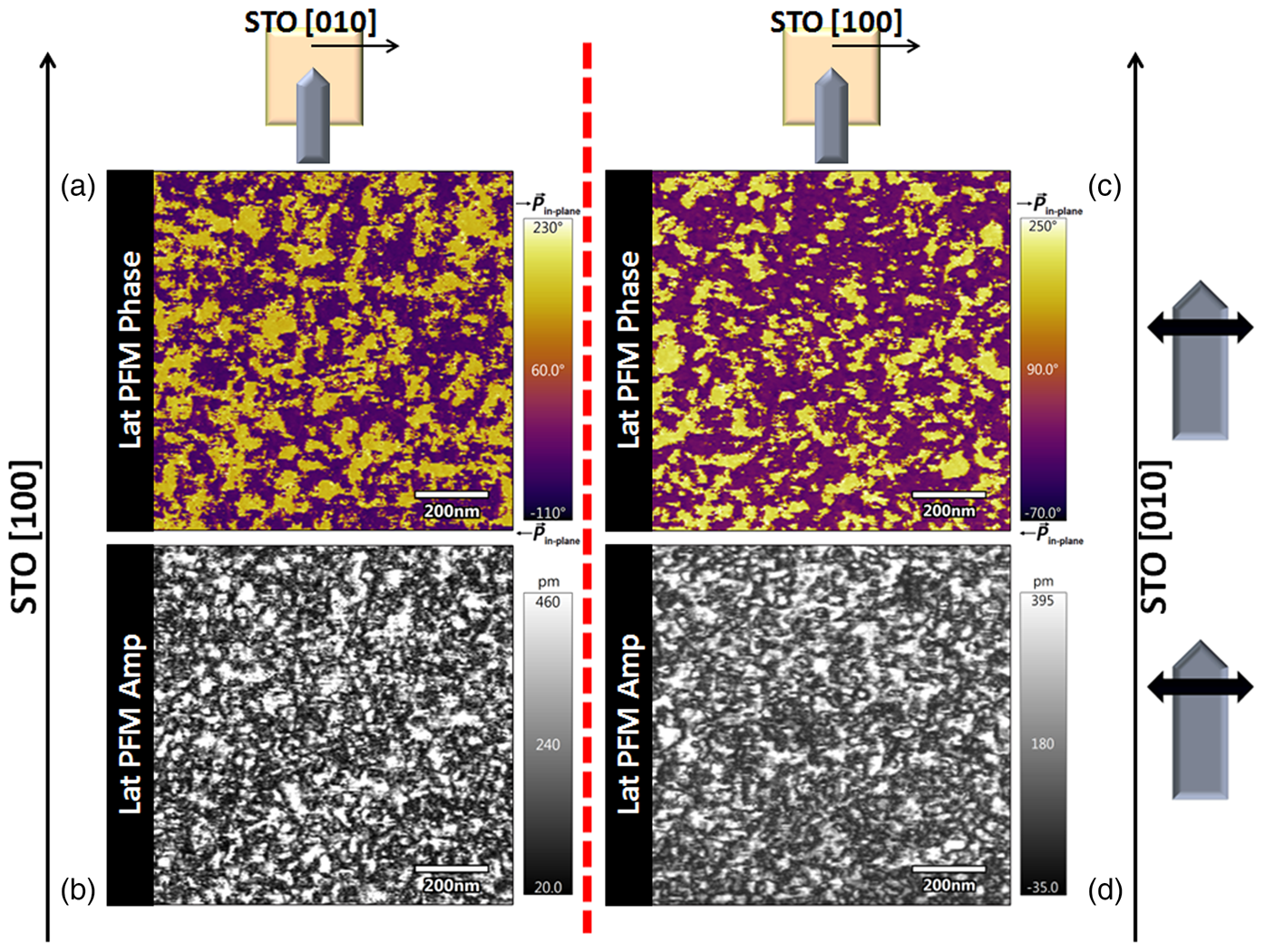
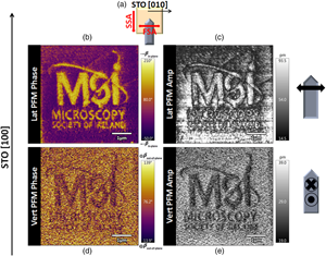
Fig. 5. Representative DART-PFM images of 8 nm B6TFMO on STO(001) synthesized by DLI-CVD at 700°C where 49% excess bismuth precursor was used during the process. (a,c) Lateral (lat) PFM phase and (b,d) lateral PFM amplitude (amp) images. Images (a,b) were performed with the cantilever scanning direction parallel to the [010]STO axis. The samples were rotated 90° for images (c–d) where the cantilever scanning direction was parallel to the [100]STO axis. The orientation of the cantilever with respect to the substrate orientation is indicated at the top of the figure. The direction of motion of the PFM cantilever, as it scans the sample surface, is indicated to the right of the images. Note that there are no microscopic topographic markers on the sample surface; therefore, the exact same location could not be found after physical sample rotation by 90°. These images demonstrate the isotropic random distribution of in-plane at 8 nm thicknesses for B6TFMO on STO (100). Uniaxial ferroelectric anisotropy is not observed at this thickness.
As discussed above, the bulk of Aurivillius phase samples display the majority of their spontaneous polarization within the a-b plane, at 45° to the tetragonal a-axis (Whatmore, Reference Whatmore, Kasap and Capper2017). In one unit cell (4–5 nm) thick Aurivillius films on NGO (NdGaO3) (001) substrates, stripe domains can be observed, orientated 45° away from the crystallographic a-axis (Gradauskaite et al., Reference Gradauskaite, Campanini, Biswas, Schneider, Fiebig, Rossell and Trassin2020; Keeney et al., Reference Keeney, Saghi, O'Sullivan, Alaria, Schmidt and Colfer2020b). At decreased thickness (half a unit cell; 2 nm), Gradauskaite et al. (Reference Gradauskaite, Campanini, Biswas, Schneider, Fiebig, Rossell and Trassin2020) report stripe domains with uniaxial in-plane ferroelectric polarization along the crystallographic a-axis only and no polarization along the b-axis for Bi5Ti3FeO15 (m = 4) on NGO (001). These anisotropic domain patterns are stabilized by the underlying substrate, and the lattice mismatch is gradually lost with increasing film thickness, whereupon an isotropic random distribution of sub-resolution 180° domains was observed for 8 nm thick Bi5Ti3FeO15 films. The corresponding ferroelectric performance of the Aurivillius phases along a certain crystallographic direction is therefore thickness and substrate-dependent. Accordingly, to optimize the performance, design, and direction of applied fields on the integration of B6TFMO into devices, the anisotropic ferroelectric properties along different crystalline orientations must be known for a particular sample type. To examine whether ferroelectricity is anisotropic within the lateral plane in bismuth-rich 8 nm thick B6TFMO, PFM experiments were performed with the cantilever aligned parallel to the [010] substrate direction (Figs. 5a, 5b). This was immediately followed by PFM experiments after rotation of the sample by 90° so that the cantilever was aligned parallel to the [100] substrate direction (Figs. 5c, 5d). In line with previous reports of the Aurivillius films (Gradauskaite et al., Reference Gradauskaite, Campanini, Biswas, Schneider, Fiebig, Rossell and Trassin2020; Keeney et al., Reference Keeney, Saghi, O'Sullivan, Alaria, Schmidt and Colfer2020b), experiments reveal an isotropic random distribution of in-plane domains in the bismuth-rich 8 nm B6TFMO films on both STO (100) and LSAT (100) substrates in the [010] and [100] substrate directions. Uniaxial ferroelectric anisotropy is not observed on these substrates at this thickness.
An in-plane electric field can be generated from the trailing field left in the wake of PFM scanning with an applied DC bias, V DC (Jesse et al., Reference Jesse, Baddorf and Kalinin2006; Balke et al., Reference Balke, Choudhury, Jesse, Huijben, Chu, Baddorf, Chen, Ramesh and Kalinin2009; Imai et al., Reference Imai, Cheng, Xin, Eliseev, Morozovska, Kalinin, Takahashi, Lippmaa, Matsumoto and Nagarajan2013; Vasudevan et al., Reference Vasudevan, Matsumoto, Cheng, Imai, Maruyama, Xin, Okatan, Jesse, Kalinin and Nagarajan2014; Gradauskaite et al., Reference Gradauskaite, Campanini, Biswas, Schneider, Fiebig, Rossell and Trassin2020; Keeney et al., Reference Keeney, Saghi, O'Sullivan, Alaria, Schmidt and Colfer2020b). As explained by Vasudevan et al. (Reference Vasudevan, Matsumoto, Cheng, Imai, Maruyama, Xin, Okatan, Jesse, Kalinin and Nagarajan2014), when the PFM tip is moved from one location to another during scanning in the presence of a DC bias, the symmetry of the field applied at the PFM tip is broken, leading to a net electric in-plane field (“trailing field”) aligned along the slow scan axis (SSA) of the cantilever. The local polarization will attempt to align along the net electric field direction, with local dipoles coupled to the crystallographic symmetry of the sample. When a high enough DC voltage is applied to the PFM tip in contact with the film surface, the domain switching process is initiated, domain walls become mobile, and larger switched domains can be generated. The PFM lithography technique can be applied in this manner to modify the ferroelectric polarization of a sample, enabling domain arrays and complex patterns to be “written” without changing the surface topography. Beginning with an unpoled condition (pristine surface), then by aligning the <100> axis of B6TFMO underneath the PFM tip to the trailing field direction, lateral poling and reversal of the ferroelectric domains can be accomplished, as shown in Figure 6. By scanning downward with the application of −7 V DC to the background and by performing PFM lithography using +7 V DC to draw the “Microscopy Society of Ireland (MSI)” logo, the in-plane components of the electrostatic field produced by the probe aligned along the SSA enable switching of the in-plane polarization components (Fig. 6a). Following the previously described “write step,” the surface was subsequently re-imaged by a probing signal, V AC, to perform the “read step.” Figure 6 displays the PFM lithography pattern generated by probing (reading) in the lateral (Figs. 6b, 6c) and vertical (Figs. 6d, 6e) directions. Despite the presence of trace levels of impurity phases, domain wall motion was not hindered by possible pinning effects, and clear ferroelectric switching was achieved for the samples prepared with 49% excess bismuth precursor, similar to prior local switching of ferroelectric domains in B6TFMO synthesized with an excess of 5% bismuth precursor (Keeney et al., Reference Keeney, Saghi, O'Sullivan, Alaria, Schmidt and Colfer2020b). Anti-parallel polarization states are observed, with 180° phase contrast between the oppositely orientated in-plane domains (Fig. 6b). At the beginning of the poling experiment, the PFM cantilever is positioned at the top of the images shown and proceeds in line-by-line scanning, where each line is scanned back (retrace) and forth (trace) along the fast scan axis (FSA). The cantilever moves down to the next and subsequent lines along the SSA (Fig. 6a). Initially, −7 V DC is applied to the sample surface and a decreased piezoresponse is observed (dark contrast) at the top of the lateral PFM amplitude image (Fig. 6c). Further down the SSA, when the PFM tip is instructed by the bias map to perform patterning of the MSI logo, both negative (−7 V DC) and positive biases (+7 V DC) are applied along the FSA. The local polarization will endeavor to align along the net electric field direction and the last field that the domain experienced (Vasudevan et al., Reference Vasudevan, Matsumoto, Cheng, Imai, Maruyama, Xin, Okatan, Jesse, Kalinin and Nagarajan2014). Here, the positive bias (+7 V DC) utilized to write the MSI logo yields an increased PFM amplitude response (Fig. 6c). However, the trailing field generated by the PFM tip is not perfectly unidirectional, and we note that the amplitude contrast for the narrower features and letters within the MSI logo is not very well refined in the lateral amplitude images. We also observe that the background piezoresponse toward the bottom of the lateral PFM image (Fig. 6c) has become complicated by the preceding dual fields applied and overall exhibits a white amplitude contrast, instead of a dark contrast expected from a uniform negative tip bias. Nevertheless, the clear 180° phase contrast between oppositely orientated domains (Fig. 6b) provides proof that stable in-plane domains can be switched by the PFM lithography experiment. As expected by Aurivillius crystal symmetry, switching of the out-of-plane polarization components is also enabled by the vertical electric field generated by the tip. Here, the vertical field applied is more unidirectional compared with the trailing field; therefore, opposite amplitude contrasts between the background (poled with −7 V DC) and MSI logo (poled with +7 V DC) are observed (Fig. 6e). As expected however, overall higher responses are observed in the lateral, in-plane direction (Fig. 6c), compared with the vertical, out-of-plane direction (Fig. 6e) where there is only a minor polarization component present along the c axis.
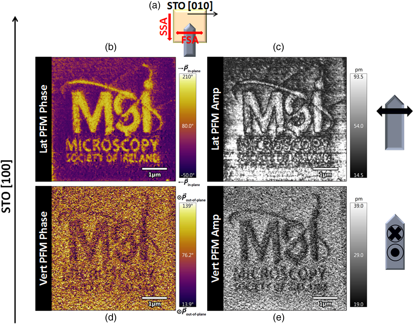
Fig. 6. Representative DART-PFM lithography images of 8 nm B6TFMO on STO (100) synthesized by DLI-CVD at 700°C where 49% excess bismuth precursor was used during the process. (a) The orientation of the cantilever with respect to the substrate orientation is indicated along with the FSA and SSA of the cantilever during scanning. Poling and reversal of the ferroelectric domains was performed by aligning the <100> axis of B6TFMO underneath the PFM tip to the trailing field direction. By scanning downward with the application of −7 V DC to the background and by performing PFM lithography at room temperature using +7 V DC to draw the “MSI” logo, the in-plane components of the electrostatic field produced by the probe aligned along the SSA enabled switching of the polarization components. (b–e) The “read” step was subsequently performed after the poling step using a probing signal (V AC) of 2.0 V. (b,c) Lateral (lat) PFM phase and lateral PFM amplitude (amp) images, respectively. (d,e) Vertical (vert) PFM phase and vertical PFM amplitude images, respectively. The direction of motion of the PFM cantilever, as it scans the sample surface, is indicated to the right of the images. These studies demonstrate the stable in-plane ferroelectric switching behavior for 8 nm thick B6TFMO.
We stress that the source of the lateral PFM signal in these ~8 nm films is positively field-induced piezoelectric strain. The fact that the vertical PFM response of the poled areas shows a very weak response in comparison (Figs. 6d, 6e) would oppose an argument that the source of the PFM signals could have non-ferroelectric electrostatics in origin (e.g., trapped charges, oxygen vacancy migration, and surface charging), since electrostatics, which can either affect the cone of the tip or the cantilever, tend to exert forces in the vertical direction (Vasudevan et al., Reference Vasudevan, Matsumoto, Cheng, Imai, Maruyama, Xin, Okatan, Jesse, Kalinin and Nagarajan2014). It is established that electrostatic forces provide a minimal contribution to the in-plane response (Jesse et al., Reference Jesse, Baddorf and Kalinin2006). Therefore, we confirm that the PFM signals observed in these ~8 nm B6TFMO samples are induced by the ferroelectric properties of the material.
Conclusions
This work demonstrates the recent progress in the optimization of B6TFMO materials toward achieving the ultimate goal of room temperature single-phase multiferroic behavior at sub-10 nm length scales. By utilizing an excess (49%) of bismuth precursor within the established (Deepak et al., Reference Deepak, Zhang, Keeney, Pemble and Whatmore2013, Reference Deepak, Carolan, Keeney, Zhang, Pemble and Whatmore2015a, Reference Deepak, Carolan, Keeney, Pemble and Whatmore2015b) growth window for a scalable DLI-CVD bismuth self-limiting process, B6TFMO films were achieved that enabled as much as a 200-fold reduction in (Mn, Fe)3O4 spinel ferrimagnetic impurity phases, compared with films synthesized with only 5% bismuth precursor excess. XRD studies demonstrate enhanced film crystallinity using this larger bismuth precursor excess, and no evidence for Bi2O3 impurity was observed within the detection level of the instrumentation.
PFM studies enabled local ferroelectric investigations of the B6TFMO films and revealed that both in-plane and out-of-plane piezoelectric domains are stable in the ~8 nm thick B6TFMO films. Despite the presence of non-ferroelectric secondary phases, domain wall motion was not hindered at a local scale by possible pinning effects, and clear ferroelectric switching was achieved for samples prepared with both 5 and 49% excess bismuth precursor. The orientation of the ferroelectric polarization can be switched, and arrays can be “written” and “read” to demonstrate states which permit anti-parallel information storage in ultra-thin B6TFMO. As expected by crystal symmetry, higher responses are observed in the lateral direction in B6TFMO. In-plane ferroelectric switching in sub-10 nm B6TFMO demonstrates its potential for use in technologically competitive data storage devices based on in-plane tunnel junctions. Given that ferroelectric polarization is parallel to the surface for all lateral directions (Vasudevan et al., Reference Vasudevan, Matsumoto, Cheng, Imai, Maruyama, Xin, Okatan, Jesse, Kalinin and Nagarajan2014), devices based on in-plane memory architectures would not be hindered by competing depolarization fields (Denev et al., Reference Denev, Lummen, Barnes, Kumar and Gopalan2011) upon scaling down to ultra-thin dimensions, meaning that higher ON:OFF tunneling current ratios can be achieved with non-destructive read operations (Chang et al., Reference Chang, Liu, Lin, Wang, Zhao, Zhang, Jin, Zhong, Hu, Duan, Zhang, Fu, Xue, Chen and Ji2016; Liu et al., Reference Liu, Chang, JI, Chen and Fu2018; Shen et al., Reference Shen, Liu, Chang and Fu2019a, Reference Shen, Fang, Tian and Duan2019b).
We acknowledge that although possible domain wall pinning by trace levels of impurities did not prevent local, microscopic PFM switching of lateral ferroelectric domains in B6TFMO, microstructural resistance to domain-wall motion may be an issue for macroscopic ferroelectric measurements. Furthermore, given that even trace (0.02–0.31 vol%) levels of ferrimagnetic impurities within the films would complicate attempts to measure a magnetic signal intrinsic to the main B6TFMO Aurivillius phase, optimization work will continue in order to completely eradicate their presence. Further explorations of optimal bismuth precursor excess will be investigated along with the most advantageous DLI-CVD growth temperatures to counteract bismuth migration and decrease the associated segregation of impurities. The potential to incorporate an ultra-thin, phase pure, room temperature multiferroic film as the tunneling layer offers the prospect of producing eight-state information storage based on simultaneous magnetoresistance and electroresistance (Yang et al., Reference Yang, Tang, Ye, Zhou, Zheng, Tang, Zhang and He2007). This is recognized within the multiferroics community as a challenge (Spaldin & Ramesh, Reference Spaldin and Ramesh2019); however, realization of this would facilitate a paradigm shift in memory storage technologies.
Acknowledgments
The authors acknowledge the support of the Royal Society-Science Foundation Ireland University Research Fellowships UF 140263, URF\R\201008, Enhancement Award RGF\EA\180206, and Science Foundation Ireland Frontiers for the Future Project 19/FFP/6475.


 Open access