Introduction
Heterostructure Field Effect Transistors (HFETs) based on AlGaN/GaN material system are expected to offer superior performance in microwave and optical communication systems [Reference Pearton and Kuo1,Reference Nakamura2]. AlGaN/GaN HFETs grown on sapphire and silicon carbide substrates with impressive DC and microwave characteristics demonstrated [Reference Gaska, Chen, Yang, Osinsky, Khan and Shur3,Reference Ping, Chen, Yang, Khan and Adesida4].It is important to know the low frequency noise since it is the limiting figure for all kinds of HEMTs and MOSFETs. Especially when these devices are used as oscillators or mixers, low-frequency noise limits the phase-noise characteristics and degenerates the performance of the electronic system. It was shown that the level of the low frequency noise strongly depends on the gate leakage current Ig even at Ig/ Id <10−4−10−5. (Id is the drain current) [Reference Levinshtein, Rumyantsev, Gaska, Yang and Shur5,Reference Rumyantsev, Levinshtein, Gaska, Shur, Yang and Khan6]. Recently, novel AlGaN/GaN Metal-Oxide-Semiconductor Heterostructure Field Effect Transistors (MOS-HFETs) with high-quality SiO2/AlGaN interfaces have been demonstrated [Reference Asif Khan, Hu, Simin, Lunev, Yang, Gaska and Shur7]. The devices had output characteristics similar to AlGaN/GaN HFETs. However, the introduction of SiO2 reduced the gate leakage by approximately six orders of magnitude, which is extremely important for high-power and low noise applications.
Device Properities
Figure 1 shows the schematic device structures of the MOS-HFETs and the base line HFETs. The AlGaN/GaN heterostructures were grown by Metal Organic Chemical Vapor Deposition (MOCVD) on (0001) sapphire and conducting 6H-SiC substrates. A 50 nm AlN buffer layer was first grown on the substrate followed by the deposition of a 1.5 and 0.5 μm semi-insulating GaN layer for sapphire and SiC, respectively. The heterostructures were capped with a 30-nm Al0.2Ga0.8N barrier layer, which was doped with silicon to approximately to 2×1018 cm−3. Both MOS-HFET and HFET devices were fabricated on the same wafer having the electron sheet density and the Hall mobility close to 9×1012 cm−2 and 1000 cm2/Vs, respectively. For MOS-HFET structures, a 100 nm SiO2 layer was deposited on the AlGaN/GaN heterostructure using plasma enhanced chemical vapor deposition (PECVD) on one half of the wafer. We studied 100 μm wide transistors with 10 μm gate length and 30 μm source-drain spacing. The large gate area and thick SiO2 were chosen in order to study the gate leakage effects on the low frequency noise in both types of devices.

Fig. 1. Schematics of AlGaN/GaN HFET and MOS-HFET structures.
The input current-voltage characteristics of the MOS-HFET and HFET on sapphire are presented in Figure 2. The threshold voltages were -15V and -3V, and subthreshold ideality factors are 6.41 and 4.54 for the MOS-HFETs and the HFETs, respectively. The maximum gate current in the MOS-HFET was on the order of 10 pA, which was several order of magnitude smaller than in the HFET . The maximum transconductance, gm = 26.5 mS/mm and 45.5 mS/mm were measured for MOS-HFET and HFET, respectively.
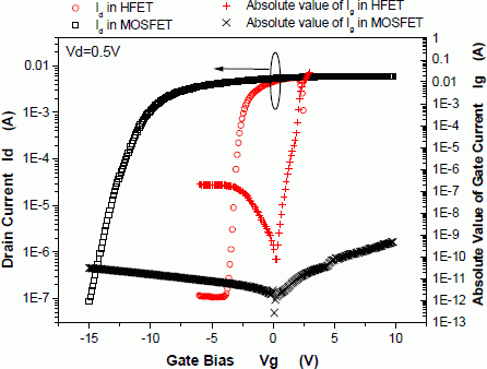
Fig. 2. Comperative input characteristics of the MOS-HFET and base line HFET.
Low Frequency Noise Measurement
Figure 3 shows the frequency dependencies of the relative Spectral Noise Density (SND) in MOS-HFET and HFET structures under different biasing conditions. The figure clearly reveals that the low-frequency noise in both MOS-HFET and HFET is a typical 1/f noise for all bias conditions. The noise level in different materials is usually characterized by the dimensionless Hooge parameter, α [Reference Hooge8]:

where f is the frequency, N is the total number of carriers in the channel between source and drain. Note that we used the the total number of carriers in the channel between source and drain not only beneath the gate since there was no significant effect of the gate with 0V bias on the channel. The latter case would give an α parameter about 10−4 which is comparable to the lowest reported ones. The devices exhibited the same noise level at the gate bias Vg = 0 V resulting the Hooge parameter α = 8× 10⁻⁴. This value of α is somewhat less than the reported values in Ref. [Reference Rumyantsev, Levinshtein, Gaska, Shur, Yang and Khan6,Reference Rumyantsev, Levinshtein, Gaska, Shur, Khan, Yang, Simin, Ping and Adesida9,Reference Kuksenkov, Temkin, Gaska and Yang10] for HFETs grown on sapphire. Lower values for α were also reported [Reference Garrido, Calle, Munoz, Izpura, Sanchez-Rojas, Li and Wang11,Reference Balandin, Morozov, Cai, Li, Wang, Wijertane and Viswanathan12].

Fig. 3 Frequency dependence of Spectral Noise Density (SND) in MOS-HFET and HFET structures on sapphire. Vd = 0.5V S/D=30 μm
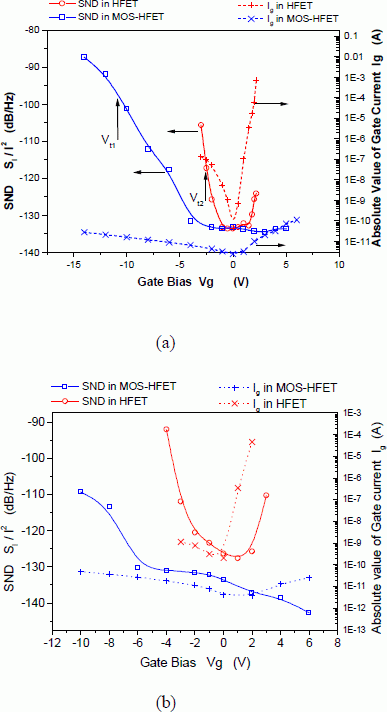
The Figure 4 compares the gate bias dependence of the SND at the frequency f = 200 Hz and the gate current in MOS-HFET and HFET. A similar level of the lowfrequency noise at zero gate bias in both types of structures indicates that no traps or defects, which might degrade the device performance, were introduced by oxidation. MOS-HFETs and HFETs demonstrated rather different noise characteristics under applied gate bias. HFETs on the sapphire and SiC substrates exhibited the similar noisegate bias dependence except for the somehow higher value for HFET on SiC at 0V gat bias. The sharp increase in noise density in HFET was attributed to the high gate leakage current at high gate biases as in Ref. [Reference Levinshtein, Rumyantsev, Gaska, Yang and Shur5,Reference Rumyantsev, Levinshtein, Gaska, Shur, Yang and Khan6,Reference Rumyantsev, Levinshtein, Gaska, Shur, Khan, Yang, Simin, Ping and Adesida9]. Some authors explained the similar gate bias dependence of the noise by the screening effect [Reference Rumyantsev, Levinshtein, Gaska, Shur, Khan, Yang, Simin, Ping and Adesida9]. However, as it is seen from Figure 4, the noise in HFET increases not only for negative gate voltage Vg but also for positive Vg . That increase can not be explained by the screening effect. It should be also mentioned that HFETs on the same substrate with identical current voltage characteristics but with a higher level of the gate leakage current Ig had a higher noise.

Fig. 4. . Gate bias dependence of the noise density at f = 200 Hz and the gate current in MOS-HFET and HFET on (a) sapphire (b) n-SiC. Vd = 0.5 V. Also shown the threshold voltages Vt1 and Vt2 , for MOS-HFET and HFET, respectively.
MOS-HFET structures had an extremely low gate leakage current and practically no gate voltage dependence for small values of the gate bias, Vg (see Fig. 4.). However for the Vg < -5V the noise in the MOS-HFET increases sharply. On the other hand, as seen in Fig. 4b, the MOS-HFET structures on SiC presented almost the same noise level with their counterparts on sapphire in 0 V gate bias but the noise continued decreasing slightly with increasing positive bias. Further experiments are needed in order to establish the nature of the noise dependence on the gate bias and/or on the drain current.
We also measured the dependence of SND on sheet electron density in the heterostructures grown on 6H-SiC using the conducting substrate as a back-gate. This allowed us to modulate the electron density in 2D gas at AlGaN/GaN heterointerface. The obtained results in Figure 5 demonstrate that the substrate bias may reduce SND by more than order of magnitude.

Fig. 5 Variation of the SND with the modulation of the substrate voltage VSub applied on the n-SiC .1)VSub = −4V, 2) VSub = +2V, 3) VSub = −2V, 4) VSub = 0V
Conclusion
In conclusion, we present the comparative low-frequency noise analysis in SiO2/AlGaN/GaN MOSFETs and base line HFETs. The low frequency noise in these MOSFETs with extremely low gate leakage current is less than HFETs at both positive and negative gate biases. That makes the novel MOSFET structure a promising device for high frequency, low noise applications.
Acknowledgements
This work was supported by the Office of Naval Research. Project monitor is Dr. J. Zolper. The authors are grateful to Professor M. E. Levinshtein and S. Rumyantsev for valuable discussions.