


Introduction
Gallium nitride is an attractive wide bandgap semiconductor material for high-temperature/high-power electronics and UV/visible optoelectronics. Recently significant progress has been made in fabrication of III-V-nitride-based laser diodes and blue/UV LEDs [Reference Nakamura1-Reference Molnar, Singh and Moustakas4]. This progress was mainly based on the achievement of controlled GaN p-doping during MOCVD epitaxial growth followed by dehydrogenation annealing to activate the Mg-acceptors [Reference Amano, Kito, Hiramatsu and Akasaki5].
It is well known that ion implantation can be used to make devices based on the wide bandgap semiconductors such as silicon carbide [Reference Kalinina and Kholujanov6]. This method allows to form selective doped regions with different and exactly controlled profiles of impurities and the concentration of these impurities is not limited by their solubility. This fact is especially important for creation of the high p-type conductivity in wide bandgap semiconductors that is connected with the relatively deep ionization levels for acceptor impurities in such materials [Reference Akasaki, Amano, Koide, Kotaki and Manate7]. For GaN, the problem of the high p-type conductivity is also complicated by high background shallow donor concentration due to native defects and the acceptor impurities passivation by hydrogen incorporating from the growth ambient [Reference Perlin, Gorczyca, Christensen, Grzegory, Teisseyne and Suski8, Reference Davis9]. To date there has been a little work in the area of the device applications of ion implantation in GaN, and generally ion implantation has been used to introduce impurities in GaN for study of their optical properties as well as the damage and passivation processes in GaN [Reference Tan, Williams, Zou, Cockayne, Pearton and Stall10]. Recently, both n- and p-type GaN, as well as semi-insulating (sheet resistance of ≥5×10⁹ W/) GaN have been demonstrated by using Si, Mg/P and N ion implantation, respectively, to MOCVD grown GaN with subsequent annealing at 1000-1100°C for 10 s [Reference Pearton, Vartuli, Zolper, Yuan and Stall11]. In this report, the sheet p-type doping of 9.4×1011 cm−2 has been achieved at 1100°C annealing with a Mg activation percentage of ∼62%, since only 1.53×1012 cm−2 of the 5×1014 cm−2 implanted acceptors were ionized assuming an energy level of 150 meV for Mg. For Si implantation, the achieved sheet n-type doping of 4.25×1013 cm−2 with ∼93% activation percentage at 1050-1100°C annealing has been reported [Reference Binari, Dietrich, Keiner, Rowland, Doverspike and Wickenden12]. In addition, high-resistivity layers for increasing the Schottky barrier height were created by implantation Mg, Mg/P and Ca into n-GaN with subsequent activation annealing [Reference Matocha, Chow, Lu and Bhat13]. The only GaN device fabricated with ion implantation doping up to now is JFET with n-channel and p-gate formed by Si (100 keV, 2×1014 cm−2) and Ca (40 keV, 5×1014 cm−2) ion implantation, respectively, and a subsequent 1150°C 15 s rapid annealing to activate the implanted dopants [Reference Zolper, Shul, Baca, Wilson, Pearton and Stall14]. Unfortunately, no detailed information on obtained gate junction properties was presented in that work.
In the present work an attempt was undertaken to apply ion implantation of Mg into n-GaN with subsequent activation annealing to form the p-n structures.
Experimental Procedure
Epitaxial n-GaN layers were grown by MOCVD on 6H-SiC (0001) substrates with concentration Nd-Na = 3×1018 cm−3. The concentration of the uncompensated donors, Nd-Na, in the GaN layers was (2-3)×1016 cm−3 according to evaluation from Raman measurements like to [Reference Harima, Sakashita, Inoue and Nakashima15]. Into these n-GaN layers Mg was implanted at energy of 100 keV and at doses in the range from 1013 to 2×1016 cm−2. Samples were annealed for 10-15 s in flowing N2-gas at a temperatures in the range from 600 to 1200°C. The Ohmic contacts to n-SiC and Mg-implanted GaN were produced by vacuum thermal evaporation of Cr/Ni and Pd/Ni, respectively. Ni in the contacts was imployed as a mask during the preparation of 300 μm mesas in diameter by reactive ion plasma etching [Reference Vassilevski, Sizov, Babanin, Melnik and Zubrilov16].
The thickness of the epilayers, the position of p-n junction inside the structure as well as the absence of the buffer layer at the GaN/SiC boundary were monitored by scanning electron microscopy (SEM). The electron beam induced current (EBIC) and back scattered electron (BSE) techniques were used. Magnesium distribution profiles across the n-GaN layer after ion implantation and annealing were measured using secondary ion mass-spectroscopy (SIMS). The activation process of the Mg acceptors by post-implantation annealing was indicated with a hot point probe method. The current-voltage (I-V) characteristics under dc conditions at current densities up to 7 A. cm−2 and capacitance-voltage (C-V) characteristics at a frequency of 1 kHz were measured for resulting mesa structures at 300 K.
Results and Discussion
According to hot point probe data, the stable p-type conductivity was obtained for the samples with Mg implantation doses more than 1×1015 cm−2 and annealing temperature in the range 1000-1200°C. Mg implanted at doses less than 1×1015 cm−2 and annealed at temperatures lower than 1000°C did not produce a sharp n- to -p conversion in conductivity. The highest p-type conductivity was fixed at a dose 2×1016 cm−2 and annealing temperature 1100°C during 15 s.
Figure 1 shows SIMS Mg profiles as-implanted in n-GaN epilayer at a dose of 2×1016 cm−2 and energy of 100 keV (curve 1) and after annealing at 1100°C during 15 s (curve 2). As seen such annealing keeps all as-implanted Mg in samples with maximum Mg concentration of 7×1021 cm−3.

Figure 1. Mg depth profiles in the n-GaN epitaxial layer after ion implantation (curve 1) and after annealing (curve 2).
Figure 2 shows cross-section of the GaN p-n structure formed under such ion implantation and annealing conditions (top). BSE/EBIC signal profiles across GaN/SiC structure with p-n junction are shown in Figure 2 (bottom). According to the EBIC and BSE data no buffer was found at the GaN/SiC boundary. The thickness of epitaxial n-GaN layer obtained to be 4.5 μm. The p-n junction position was about 0.4 μm. The correct choice of the optimum parameters of measurements in SEM provided of the high precision in a determination of the position of p-n junction. Accelerating voltage was 10 keV and electron beam current was ∼ 5×10⁻¹¹ A.
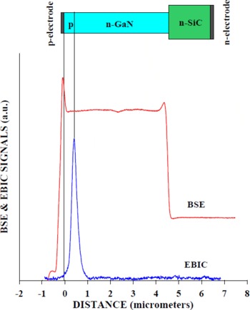
Figure 2. Cross-section of the Mg doped GaN p-n junction (top) and BSE/EBIC signal profiles across the p-n junction (bottom).
Figure 3 shows (C-V) characteristic for 300 μm p-n mesa-structures in diameter formed by Mg ion implantation at a dose of 2×1016 cm−2 at energy of 100 keV followed by annealing at 1100°C during 15 s. As follows from the analysis of (C-V) characteristics, the capacitance is proportional to the quantity (U+Uc) −1/n, where n is a constant for a given sample characterizing the stepness of (C-V) characteristic, U - the applied reverse voltage to p-n junction, Uc - the contact potentials difference. Measured value of n=3 indicates that Mg ion-doped GaN p-n junctions are nearer to linearly-graded ones. The C-V characteristics in V-C−3 co-ordinates were straight lines with cut-off voltage about 2.8 V.
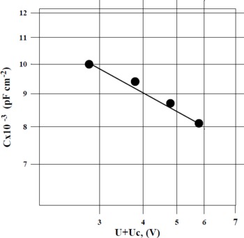
Figure 3. Capacitance-voltage characteristic for the GaN p-n junction fabricated by Mg ion implantation.
Current-voltage characteristic under dc conditions for such p-n mesa-structures is showed in Figure 4. The breakdown voltage estimated as the value of the reverse voltage corresponding to the current value of 10−6 A and was equal to 15 V. The p-n junction diodes had good rectifying properties: a rectification factor was no less than 105 at a voltage of 3V.

Figure 4. I-V characteristic of the Mg doped GaN p-n junction.
Conclusion
Conditions for ion implantation with Mg to n-GaN and subsequent annealing have been established yielding stable p-type conductivity layers. It has been shown that by ion implantation with Mg to n-GaN, p-n junctions can be obtained at a specified depth and with reproducible electrical characteristics. Rectification factor no less than 105 has been obtained for such p-n junctions. These results evidence the opportunity of investigating the fundamentals of ion implantation into III-V nitrides and develop a new technological method for device formation.
Acknowledgements
The authors thank Prof. G.F. Kholujanov for helpful consultations, M.P. Vatnik for carrying out of ion implantation and V.Yu. Davydov for Raman measurements.
This work was supported in part by the Arizona State University.


