


1. Introduction
Many important materials properties of GaN, such as impurity and exciton binding energies, effective masses, defect properties, and surface characteristics remain poorly known at present, in spite of considerable technological interest in this material. Optical spectroscopy is a highly useful tool to determine many of these properties [1]. In the following Reference Smith, Lin, Jiang and Khan[a], we describe some results of recent experimental and theoretical investigations of donor, exciton, and surface properties of GaN.
2. Theoretical Calculation Of Donor States In GaN
In a direct gap material such as GaN, hydrogenic effective mass theory ordinarily gives a good description of shallow donor levels. The wurtzite symmetry of GaN, however, requires some modification of this theory to account for possible anisotropy in the conduction band effective mass and the static dielectric constant, both of which may differ along the c-axis and perpendicular to it. We also wish to include the effects of a magnetic field for comparison with experimental measurements; the field is assumed here to lie along the c-axis. has been given, for example, by Dimmock and Wheeler in the analogous case of excitons Reference Skromme, Holloway and McGuire[2]. For convenience we adopt a normalized coordinate system (x′, y′, z′), where x′ = x/a B *, y′ = y/a B *, and z' = z (m z */m x *)1//2/a B *; a B *=a B (ε x ε z )1/2/(m x /m o ); ε x and ε z are the relative static dielectric constants in the x and z directions, respectively, where the z-direction is taken along the c-axis; m x * and m z * are the electron effective masses in those directions; a B is the hydrogenic Bohr radius; and m o is the free electron mass. We further express energy in units of the effective Rydberg R *, where R *=R(m x */m o )/(ε x ε x ), and R is the usual hydrogenic Rydberg. The magnetic field B, assumed here to lie in the z-direction, is expressed in terms of the normalized parameter γ* = (μ B B/R)(ε x ε z )/m x */m o )2, where µB is the usual Bohr magneton [= q h/(2 m o )]; a cylindrical gauge is used. Anisotropy is measured in terms of the parameter α = 1 − (ε x m x *)/ε z m z *), so that an isotropic material has α = 0 and the possible values of α range from −∞ to +1.
In this notation, the relevant normalized effective mass equation is written

where Ψ is the envelope function, E is the energy in effective Rydbergs, g ez is the electron spin g-value along the z-direction, and L z and S z are the z-components of the usual orbital and spin angular momentum operators. The terms in the Hamiltonian represent kinetic energy, the orbital paramagnetic Zeeman interaction, the diamagnetic shift, the spin energy, and the Coulomb energy, respectively. The spin energy [±(1/2) g ez µ B B] is omitted in the following. Two valid quantum numbers correspond to the z-component of angular momentum (denoted) m ℓ and to the parity (denoted q, where q=0 for even and q=1 for odd parity, respectively); a third one could be used to label the different states of the same symmetry. For clarity, we instead label the label the states by the three quantum numbers (n, ℓ, m ℓ), which are valid at zero field. The problem is then converted to cylindrical coordinates and the wave function is written in the form
where ψ(ρ,z) is even in ρ and z (although of course only ρ>0 is physically meaningful). After converting Equation (1) to cylindrical coordinates and substituting Equation (2) into it, the resulting equation is then solved numerically for various values of q and for positive values of m ℓ. States with m ℓ < 0 have energies given by
The numerical calculation is done with five-point finite differences inside a finite cylindrical box, using a grid which symmetrically straddles (but does not include) the origin. A conjugate gradient algorithm is used together with Gram-Schmidt orthogonalization and subspace diagonalization to compute several of the lowest-lying eigenvalues and wave functions simultaneously. Calculations have been carrier out for all combinations of anisotropy factors α varying from −0.4 to 0.4 in steps of 0.08 and dimensionless magnetic fields varying from γ =0 to 0.2 in steps of 0.01. All states through n=3 were included. Performing the calculation in this dimensionless way allows us to interpolate to fit experimental results for any desired materials parameters in the expected range.
The problem of an isotropic H atom in a magnetic field has been solved extensively and very accurately by many authors; we cite particularly the comprehensive results of Rösner et al. Reference Dimmock and Wheeler[3] Our results for α = 0 agree well with these for all magnetic fields studied. The absolute accuracy of our calculations for α = 0 is about 3×10⁻⁴ or fewer effective Rydbergs (about 0.01 meV for donors in GaN), lower than that of Ref. Reference Dimmock and Wheeler[3], but more than adequate compared to the present experimental resolution of ≤ 0.1 meV. (The error is higher, 0.0025 Rydbergs or less, for the 3s state.) The problem of an anisotropic donor or exciton in zero field has also been studied by highly accurate variational methods (see, e.g., Faulkner Reference Rosner, Wunner, Herold and Ruder[4] and Broeckx et al. Reference Faulkner[5]). These calculations generally considered only anisotropy in effective mass, but the anisotropy in the dielectric constant has exactly the same effect (as evidenced in the definition of α). Our results as a function of α for B=0 agree with available more accurate prior calculations to within 0.0033 Rydbergs or better.
Relatively few investigations have been made of the anisotropic problem in a magnetic field. The problem was investigated for all states through n=3 using a series expansion of the perturbing Hamiltonian in powers of α, together with first-order perturbation theory, by Dimmock and Wheeler Reference Skromme, Holloway and McGuire[2] and by Wheeler and Miklosz Reference Broeckx, Clauws and Vennik[6]. Both the anisotropy and the magnetic field were treated as perturbations. A more accurate perturbational theory was recently given for the ground state by Zhang et al. Reference Wheeler and Miklosz[7], who did not use the power series expansion in α. The perturbation results (using Ref. Reference Wheeler and Miklosz[7] for the ground state) agree with the accurate variational results for the effects of anisotropy alone to within 0.0044 Rydbergs for α =−0.37 or +0.27 (values for which literature data are available). However, they are much less accurate for the effects of magnetic field. Assuming m x * ≈ 0.22 and R * ≈ 29 for donors in GaN and a magnetic field of 11 T (γ = 0.10), the perturbation results for the magnetic field alone are in error by 0.016 and 0.22 Rydbergs (0.5 and 6.4 meV, respectively), for the 1s-2s and 1s-3s separations, respectively. The application of perturbation theory is therefore inappropriate over the range of fields commonly used.
Accurate finite difference calculations have been reported over a wide range of magnetic fields and anisotropies by Zhang et al. Reference Wheeler and Miklosz[7], but only the ground state was considered. Variational Reference Zhang, Mascarenhas and Jones[8] or variational-perturbational Reference Seiler, Heiman, Feigenblatt, Aggarwal and Lax[9] results have been given for certain specific materials (see also references in Ref. Reference Wheeler and Miklosz[7]). The present method yields as many excited states as desired for arbitrary fields or anisotropy parameters, and does not depend on knowledge of the most appropriate form of variational wave function or trial Hamiltonian in any given case.
Sample results of our calculations for the estimated anisotropy of GaN (α = 0.16, taking m x *=0.22 m o , m z *=0.24 m o , ε x =9.5, and ε z =10.4) are given in Figure 1 as a function of the dimensionless magnetic field. At zero field, the anisotropy deepens the ground state, and deepens and splits the n=2 state into separate 2p o, 2s, and 2p ± states, in order of increasing energy. The 2p o/2s splitting is 0.38 meV and the 2s/2p ± splitting is 0.18 meV, using R *= 30.3 meV, based on the same materials parameters. The n=3 state deepens and splits into separate 3p o, 3d o, 3d ±1, 3s, 3p ±, and 3d ±2 states, in order of increasing energy, but the shift and splittings are smaller (the splitting between 3p o and 3d ±2 states is 0.28 meV). (The specified orderings and splittings are for zero central cell correction, which would shift the s-states but none of the others.) Both the Zeeman splittings and diamagnetic shifts are readily apparent as a function of field. The inaccuracy of perturbation theory is also apparent in this figure, especially for the n=3 states. More complete results of the calculations will be presented elsewhere. These results can serve as the basis for detailed analysis of experimental results on donors in GaN, as described below.

Figure 1. Results of our theoretical calculation for the energy levels of a Coulombic donor state in GaN as a function of magnetic field (lines). Notation is that of isotropic H atom in low field limit. States are listed in order of increasing energy within each group in the legend (e.g., ns, 2p, 3p, 3d states). Points show corresponding perturbation theory (PT) results (only 3p - shown of n=3 states for clarity; others deviate similarly from accurate calculation).
3. Experimental Methods
The spectra to be described in the following were recorded for high quality heteroepitaxial GaN layers grown on sapphire(0001) substrates grown by HVPE at Epitronics and Lincoln Laboratories, and by MOCVD at Honeywell. The HVPE layers were 300 µm (HVPE-1, Epitronics) and 68 µm (HVPE-2, Lincoln Laboratories) thick, and the MOCVD layer was 8 µm thick. A series of 10 µm thick layers grown by HVPE at Epitronics, with intentional Si doping levels ranging from none to N D −N A = 4 × 1017 cm−3 as measured by capacitance-voltage profiling, was also studied. The undoped layer in this series had N D −N A < 1 × 1016 cm−3. Further description of the samples has been given elsewhere, along with the methods used to record the optical spectra Reference Dai, Pei and Chuu[10] Reference Skromme, Zhao, Goldenberg, Kong, Leonard, Bulman, Abernathy and Pearton[11] Reference Skromme[12] Reference Skromme, Jayapalan, Wang and Sankey[13] Reference Skromme, Jayapalan, Vaudo and Phanse[14].
Passivation and chemical treatments were performed on both HVPE and (less extensively) on MOCVD material, none of which was intentionally doped. For nonsulfide chemical treatments, the sample was dipped in a solution for 1-10 min, rinsed in deionized water (DI) and solvents and blown dry. The room temperature PL intensity was measured within five minutes after treatment. Sulfide treatments were similar, but without rinsing; the sample was simply spun dry.
4. Observation And Identification Of Shallow Donor Levels
A variety of experimental methods can be used to determine the binding energies of shallow donors. In this study, we utilize spectroscopic methods, which are based on measurements of the difference in binding energies of the ground and excited states in zero or high magnetic field.
4.1 Magnetospectroscopy of Two-Electron Transitions
Two-electron replicas, or excited final-state transitions, occur when the exciton bound to a neutral donor recombines and leaves the donor in an excited state. Their energy is therefore lower than that of the principal (Do,X) peak by the difference in ground state and excited state binding energies. The principal (Do,X) peak results when the neutral donor is left in its ground state, the most probable event. In reality, however, there is typically more than one principal (Do,X) peak, even if only one donor species is present. This effect is due to the existence of low-lying orbital excitations of the exciton about the neutral donor, which have a nonrigid rotational character Reference Jayapalan, Skromme, Vaudo and Phanse[15]. The splitting of the valence band in wurtzite material also gives rise to splitting in the (Do,X) state, which may be further complicated by interaction with the rotational splittings. Excited (Do,X) states are readily resolved only in samples with relatively narrow linewidths, and may sometimes be confused with other types of peaks such as ionized donor-bound excitons, (D+,X), or excitons bound to other defects. Each excited initial state may (depending on selection rules) exhibit two-electron replicas of its own, which tend to complicate the two-electron spectra. Direct evidence of two-electron replicas of excited (Do,X) states in GaN, in the form of thermalization data, is shown below, although the principal excited-state peaks themselves could not be clearly resolved.
Central cell corrections or chemical shifts to the purely Coulombic binding energies are largest for the ground state of the donors. All ns states show central cell corrections essentially proportional to the probability density at the origin, i.e., to n −3. All other excited states of the donors have zero shift, due to nodes at the origin. The (Do,X) states themselves (both ground and excited states) also exhibit central cell shifts, although such shifts are not always easily resolved Reference Ruhle and Klingenstein[16]. These shifts tend to be linearly proportional to those of the donor ground states, a relationship known as Haynes's rule Reference Skromme, Bhat, Cox and Colas[17]. (A similar relationship does not generally apply to shallow acceptors in direct gap semiconductors, although one is frequently incorrectly assumed.) The slope of this linear relation (denoted m) varies from material to material, depending on the electron and hole effective masses; it typically ranges from 0.14 to 0.28 (its exact value is not yet known for GaN). Considering these factors, the separation between two-electron satellites involving a given rotational state of the (Do,X) complex and different donor species is (1+m) times the difference in ground-state central-cell corrections, when the donors are left in an excited p-state. The corresponding factor is (0.889+m) when the donors are left in their 2s excited state, which is still generally greater than one. The value of m typically increases with magnetic field Reference Haynes[18]. Errors can occur when comparing two-electron spectra to infrared data if these factors are not considered Reference Ruhle and Klingenstein[16].
Two-electron transitions were first identified in GaN by Skromme et al. in 1996 Reference Dai, Pei and Chuu[10] Reference Karasyuk, Beckett, Nissen, Villemaire, Steiner and Thewalt[19], and their identification was later confirmed by other groups Reference Skromme, Hutchins, Zhao, Kong, Leonard, Bulman, Abernathy and Pearton[20] Reference Fiorek, Baranowski, Wysmolek, Pakula, Wojdak, Grzegory and Porowski[21]. Definitive evidence for the nature of these transitions was the observed Zeeman splittings in a high magnetic field Reference Dai, Pei and Chuu[10] Reference Karasyuk, Beckett, Nissen, Villemaire, Steiner and Thewalt[19], which rules out any alternative explanation such as acceptor-bound excitons. An example of this magnetic field dependence is shown in Figure 2 for a HVPE sample. At zero field (bottom spectrum), the dominant peaks at 3.4717 and 3.4726 eV are a doublet separated by 0.9 meV, corresponding to the principal (Do,X) n=1 transition. The doublet is attributed to the presence of at least two distinct donor species with different binding energies, because the relative intensities of the two components vary from spot to spot on the sample. Corresponding variations are observed in the two-electron transitions, although the exact correspondence between (Do,X) n=1 and (Do,X) n=2 peaks is not yet certain. These observations, and the absence of pronounced thermalization behavior, tend to rule out excited orbital states as the cause of the observed (Do,X) n=1 splitting. However, such excited states (apparently not resolved) do exist, as shown below from the two-electron spectra. The peaks to higher energy correspond to the ground and excited states of (primarily) the A free exciton, together with an n=2 exciton bound to a neutral donor as discussed below.
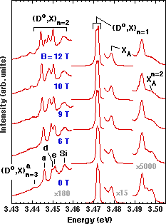
Figure 2. Excitonic 1.7 K PL spectra of the undoped Epitronics HVPE-1 300 µm GaN/Al2O3sample as a function of magnetic field in Faraday configuration with B||[0 0 0 1]. Only one of the two possible circular polarizations is detected in these spectra.
Our primary interest here is in the structure at lower energy, which we attribute to two-electron transitions where the donor is left in its n=2 or n=3 excited state, denoted (Do,X) n=2 and (Do,X) n=3, respectively. The (Do,X) n=2 transitions are believed to involve at least four distinct donor species in this sample, giving rise to the main observed fine structure. The anisotropy splittings are almost certainly too small to be resolved (see Figure 1). Binding energies of the various species can be estimated using a simple hydrogenic model, where the binding energy is just 4/3 of the separation between the strongest (Do,X) n=1 peak and each (Do,X) n=2 peak. (We neglect the splitting of the (Do,X) n=1 peak, since the detailed correspondence between principal (Do,X) and two-electron peaks is not yet clear.) We obtain values of 22, 27.5, 28.8, and 34.4 meV for the ionization energies of the Si, e, d, and a donors, respectively (a more complete listing including donors observed in other samples is given in Table I). Identification of the Si level is discussed below, and the other three levels have not yet been identified. Based on the ionization energy of the a donor derived from the n=1 to n=2 separation, we predict that the corresponding (Do,X) n=3 peak should lie 8/9 of the ionization energy below the (Do,X) n=1 peak, at 3.4411 eV. The clearly observed peak at 3.4412 eV matches this prediction very well and is therefore assigned to the n=3 state of the a donor. The n=3 peaks corresponding to the other donor species are not observable, presumably because they overlap other (Do,X) n=2 peaks.
Identification of this structure is strongly supported by the magnetic field dependence, which shows Zeeman splittings and diamagnetic shifts of the two-electron satellites, particularly for those involving the n=3 state. Small spin splittings are apparent in the principal (Do,X) peaks, which exhibit broadening and at least three subcomponents at 12 T, at 3.4712, 3.4716, and 3.4722 eV. This splitting was not detected in earlier PL measurements in Faraday configuration by Volm et al. Reference Korona, Bergman, Monemar, Baranowski, Pakula, Grzegory and Porowski[22], probably due to lower instrumental resolution and broader linewidths (1.4 meV full width at half maximum or FWHM) compared to that of the individual (Do,X) components in the present sample (0.80 meV FWHM at zero field, as determined by curve fitting). The shifts and splittings in the two-electron satellites are significantly larger, showing clearly that they are orbital and not spin in nature. Detailed interpretation of the fine structure, however, is hampered by the number of different donor species present in the sample, and by contributions from excited initial states as noted below. Samples with similar or better linewidths and a single residual donor species may be necessary to achieve a full interpretation.
Table I Spectroscopic Binding Energies

* Existence uncertain
The importance of excited (nonrigid rotator) states of the initial (Do,X) complex is illustrated by the variable temperature PL spectra at zero field in Figure 3. These spectra were recorded at a different spot on the HVPE-2 sample of Figure 2. The relative strengths of the two main components of the (Do,X) n=1 doublet have changed, implying a lateral variation in the concentration of the two donor species involved. A possible third (Do,X) n=1 component at 3.4705 eV is also resolved, which might involve a third donor species. Corresponding changes are observed in the two-electron structure. Furthermore, as the temperature is raised from 1.7 to 20 K, each component observed in the (Do,X) n=2 and (Do,X) n=3 peaks gives rise to a new component about 1.1 meV higher in energy. Splitting of the final Do states would not cause thermalization, so the splitting must originate in the initial (Do,X) state. No clear thermalization is evident in the (Do,X) n=1 region with a similar separation, however, which is probably because of overlapping peaks involving different donors and possibly differences in selection rules. Existence of excited (Do,X) states is nonetheless confirmed very strongly by this data.

Figure 3. Excitonic PL spectra of the Epitronics HVPE-1 sample as a function of temperature.
4.2 Identification of the Si Donor Level
Low temperature PL spectra for a series of HVPE samples grown at Epitronics with various intentional Si doping levels from none to 4 × 1017 cm−3 are shown in Figure 4. In the not intentionally doped sample at bottom, the two-electron replica structure gives evidence for two residual donor species, with binding energies of 28 and 34 meV. As the Si doping level is increased, a new peak at about 16.2 meV below the principal (Do,X) peak appears and increases in intensity with Si doping level. The two-electron structure is completely washed out by doping-induced broadening at the highest doping level, however. The new peak splits by about 2 meV in a 12 T magnetic field (not shown), confirming the involvement of an n=2 donor state. We attribute this new peak to a two-electron satellite involving a Si donor level, whose binding energy is estimated from a simple hydrogenic model as 22 meV. This same level appears in some (but not all) unintentionally doped HVPE samples (see, e.g., Figs. 2 and 5), where it likely originates from the interaction of HCl with the hot quartz reactor walls to form chlorosilanes, which then decompose to yield Si doping. The unusually small binding energy of this level is surprising, and will require further experimental and theoretical study. Amphoteric behavior in the form of a corresponding Si acceptor level has also been observed Reference Skromme, Jayapalan, Vaudo and Phanse[14], whose binding energy has been estimated from a conduction band-to-acceptor transition to be about 224 meV (Table I). This value is virtually identical to that we estimated previously by the same method for Mg acceptors in GaN (224 ± 4 meV) Reference Volm, Streibl, Meyer, Detchprohm, Amano and Akasaki[23]. Evidence for the Si acceptor level is in fact apparent in Figure 4, in the form of a LO phonon replica of an exciton bound to a neutral Mg acceptor, denoted (Ao,X)LO. The corresponding no-phonon peak is unresolved on the low energy side of the broadened principal (Do,X) peak, but is visible in the phonon replicas because of the characteristically larger phonon coupling of (Ao,X) transitions. Further discussion of the Si-related levels has been given elsewhere Reference Skromme[12] Reference Skromme, Jayapalan, Vaudo and Phanse[14].

Figure 4. Excitonic 1.7 K PL spectra of four Epitronics HVPE samples with various Si doping levels. Lowest spectrum is for undoped sample; next lowest is for sample with ND -NA = 5 × 1016 cm−3; second from top is for sample with ND -NA = 2.5 × 1017 cm−3; top spectrum is for sample with ND -NA = 4 × 1017 cm−3.
4.3 Electronic Raman Scattering from Shallow Donors
An alternative method to study shallow donors is electronic Raman scattering (ERS), in which an incident photon scatters inelastically from a neutral donor, leaving the donor in an excited state. The scattered photon therefore has a Stokes shift relative to the incident photon by the difference in energy between the ground and excited state. This process is much weaker and more difficult to detect than luminescence, but has the advantage that the spectra are not directly tied to the complicated (Do,X) system with its multiple excited states, and are therefore simpler. Moreover, the internal excitation energies of the donors are not sensitive to strain, to first order, so that a major inhomogeneous broadening mechanism of the (Do,X) peaks and their two-electron satellites is eliminated. The strength of the ERS process can be drastically increased by using incident laser photon energies close to that of the (Do,X) energy, which produce a resonance in the scattering cross section. Except very close to resonance, selection rules permit only scattering from the 1s ground state (the only occupied at equilibrium) to even parity excited states, principally the ns states (2s, 3s, etc.). The ERS spectrum should therefore exhibit a subset of the states observed in PL, and is basically complementary to far-infrared absorption, where a change in parity is required. The choice of photon energy in the present study is based on the available Ar+ laser lines, of which we use the 3.407 eV line just below the band gap to minimize excitation of PL emission while providing significant resonant enhancement.
An example of an ERS spectrum is shown as the upper curve in Figure 5, using the

Figure 5. Shifted Raman spectrum (upper) and PL spectrum (lower) of the Lincoln Laboratories HVPE-2 sample; actual laser energy during the Raman measurement was 3.407 eV. The ERS peaks are denoted
To confirm the assignment of these peaks, their dependence on magnetic field was measured as shown in Figure 6. Both peaks, along with a peak due to a third donor species which becomes clearly resolved only at high field, shift monotonically to lower energy while the vibronic E2 phonon peak does not move. The peaks also become narrower, which may be due to shrinkage of the wave functions and reduced inhomogeneous Stark effect broadening. The existence and direction of the shift is consistent with the diamagnetism expected for 1s−2s scattering, as is the absence of observable splitting. The magnitude of the shift is significantly smaller than expected for an electron mass of 0.22 m o perpendicular to the c-axis, for reasons that are not yet clear. The existence of the shift, however, confirms the nature of the process.

Figure 6. Electronic Raman spectra [
The only other evidence for ERS in GaN has been obtained in resonance with the deep level yellow transition in cubic Reference Johnson, Yu, Boney, Hughes, Cook, Schetzina, Zhao, Skromme and Edmond[24], mixed-phase Reference Johnson, Yu, Boney, Hughes, Cook, Schetzina, Zhao, Skromme and Edmond[24], or hexagonal Reference Ramsteiner, Menniger, Brandt, Yang and Ploog[25] GaN. These spectra were however much more complicated than the present ones, and their assignment to shallow donors in GaN has been controversial Reference Jiang, Ramsteiner, Ploog, Tews, Graber, Averbeck and Riechert[26] Reference Siegle, Loa, Thurian, Eckey, Hoffmann, Broser and Thomsen[27]. The simplicity of the present spectra, their correlation with two-electron satellites observed in PL, and their behavior in a magnetic field all support their assignment to the ERS mechanism.
4.4 Comparison with Other Measurements
Most other spectroscopic studies of donors in GaN have used infrared absorption, at zero Reference Ramsteiner, Menniger, Brandt, Yang and Ploog[28] Reference Meyer, Volm, Graber, Alt, Detchprohm, Amano and Akasaki[29] and high magnetic fields up to 10 T Reference Meyer[30] or 27 T Reference Moore, Freitas and Molnar[31]. The results are summarized in Table I. The zero field measurements on undoped HVPE material showed evidence for a 34.5 meV donor and possibly traces of deeper donors Reference Ramsteiner, Menniger, Brandt, Yang and Ploog[28] Reference Meyer, Volm, Graber, Alt, Detchprohm, Amano and Akasaki[29], while extrapolation of a very broad (∼5.6 meV FWHM) absorption observed at fields of 13-27 T in one Si-doped MOCVD layer yielded an estimated donor binding energy of ~29 meV Reference Moore, Freitas and Molnar[31]. This value is quite different from our determination of the Si binding energy; a possible explanation is that the species observed in that work was actually a residual donor rather than Si. Magnetic field studies of undoped HVPE material showed evidence of 1s-2p ± transitions for two residual donors having estimated binding energies of 31.1 and 33.8 meV Reference Meyer[30]. An additional peak at 17.0 meV, independent of magnetic field, was assigned to the 1s-2p o transition of the 31.1 meV donor Reference Meyer[30], but the theoretical calculations presented above show that this assignment cannot be correct. On the other hand, this peak is quite close to the n=1/n=2 splitting we observed for Si donors, suggesting it might involve our ~22 meV level. Further work will be necessary to confirm this association.
Variable-temperature Hall effect measurements have also been used to estimate donor binding energies in GaN Reference Wang, Kaplan, Ng, Doverspike, Gaskill, Ikedo, Akasaki and Amono[32] Reference Wickenden, Rowland, Doverspike, Gaskill, Freitas, Simons and Chi[33]. Binding energies of 12-17 meV Reference Wickenden, Rowland, Doverspike, Gaskill, Freitas, Simons and Chi[33] or 26 meV Reference Wang, Kaplan, Ng, Doverspike, Gaskill, Ikedo, Akasaki and Amono[32] were determined for Si donors in Si-doped material. However, the thermal activation energy measured by Hall effect is affected by screening and banding of the higher excited states of the impurities, and by merging of this band with the conduction band edge. The conduction band edge is effectively lowered by the doping Reference Gotz, Johnson, Chen, Liu, Kuo and Imler[34], yielding a thermal activation energy which is a function of the doping level. It typically varies as
where α is a constant. The spectroscopically measured binding energy is generally independent of doping where it can be determined Reference Gotz, Johnson, Chen, Liu, Kuo and Imler[34], and is therefore more reliable. The Hall effect values can be distorted if multiple donor species are present, and require several decades of freeze-out to be highly reliable.
5. Free Exciton States at Low and Room Temperature
There has been considerable controversy over the binding energy of the free excitons in GaN, which is important in assessing their contribution to the optical properties of this material. Reported values have ranged from ~18 to 27 meV (Table I). Many of the lower values may be due to misassignments of low temperature PL spectra, as discussed elsewhere Reference Dai, Pei and Chuu[10]. Most determinations have been based on the observed separation between n=1 and n=2 states observed in PL and/or reflectance. The observation of Zeeman splitting and the expected strong diamagnetism of the PL feature assigned to the n=2 state of the A free exciton, together with the observation of a corresponding feature in reflectance, provided the strongest evidence for this process Reference Dai, Pei and Chuu[10] Reference Karasyuk, Beckett, Nissen, Villemaire, Steiner and Thewalt[19].
A remaining question has been whether the free exciton binding energies depend on strain, due to valence band mixing. Data demonstrating clearly that the A exciton binding energy does not are given in Figure 7. The three PL spectra in the lower portion of this figure were recorded on samples with significantly different strains; those of the HVPE-2 and MOCVD layers have been shifted by +0.0004 and −0.0135 eV to align the

Figure 7. Reflectance spectrum of Epitronics HVPE-1 sample (top), and PL spectra of HVPE-1, the Lincoln Labs HVPE-2 sample, and an MOCVD sample (bottom three, listed from top to bottom).
The reflectance spectrum of Figure 7 was recorded in the conventional geometry, with the incident and reflected light traveling nearly parallel to the c-axis (σ polarization) and reflecting from the front surface of the epilayer. Thick HVPE layers permit reflectance to be performed on the edge of the epilayer as well, which allows detection of both σ and π-polarized light. An early study of this type by Dingle et al. Reference Yamaguchi, Mochizuki, Sunakawa and Usui[36] showed evidence of the correct selection rules (the A exciton is forbidden in π-polarization) and the expected change in oscillator strengths (the relative strengths of the B and C excitons are interchanged from σ to π polarization Reference Dingle, Sell, Stokowski and Ilegems[37]). We recently performed a similar experiment using an HVPE layer of improved quality compared to the early work, yielding better resolved and more detailed spectra which reveal excited states of the excitons, as shown in Figure 8. The σ-polarized spectrum from the layer edge is similar to the front surface reflectance spectrum of the same sample in Figure 7. However, the strain is a little different (presumably due to averaging over the epilayer thickness in the edge case) and the spectrum is a little broader in Figure 8, perhaps due to the strain gradients. In the π-polarized case, the A exciton nearly disappears (and disappeared entirely when a single piece was used rather than the sandwich configuration of Figure 8). The C exciton is however much stronger relative to B as expected theoretically, and the n=2 C exciton can even be discerned. Fitting and quantitative analyses of these spectra is currently in progress, but they clearly confirm the identification of the A, B, and C excitons and their qualitatively expected oscillator strengths. We have made similar successful measurements at room temperature, which will be reported elsewhere.

Figure 8. 1.7 K reflectance spectrum of Epitronics HVPE-1 sample recorded from the edge of the sample (see inset) in two orthogonal linear polarizations (upper spectrum, σ -polarization; lower spectrum, π-polarization).
The nature of the band edge PL recombination process at room temperature in GaN has been controversial. Comparisons of excitonic features observed in photoreflectance with PL measurements as a function of temperature gave strong evidence that the recombination is excitonic Reference Bir and Pikus[38] Reference Chichibu, Azuhata, Sota and Nakamura[39], but other, less direct arguments have been made in support of band-to-band recombination Reference Tchounkeu, Briot, Gil, Alexis and Aulombard[40]. In Figure 9, we show a room temperature simple (not modulated) reflectance spectrum of a 10 µm thick undoped HVPE sample, together with a PL spectrum at that temperature. The simple reflectance spectrum is, we believe, the first reported observation of excitons in GaN at room temperature by this method. Both unresolved A and B excitons and a weak feature due to C excitons are detected. The first feature matches the PL peak position exactly, rather than being displaced 26.4 meV lower as it would if the PL were band-to-band recombination. The linewidth of the free exciton feature is only 32.5 meV FWHM (and is even lower, 28 meV in the MOCVD layer of Figure 7; not shown). These values are substantially smaller than the minimum theoretical value for band-to-band transitions, about 1.8k B T or 46.1 meV. The comparison with reflectance and the PL linewidth prove conclusively that the recombination is excitonic, not band-to-band. We also observe two shoulders on the low energy side of the XA/B PL peak, which we attribute to XA/B recombination with the simultaneous emission of one or two LO phonons. These low energy replicas are observed with approximately the same strengths in virtually all samples, ruling out their association with impurities or other extrinsic causes. We attribute the persistence of excitonic recombination to room temperature in GaN mainly to the large energy of the LO phonon (about 92 meV). The LO mode is therefore relatively weakly populated at room temperature and hence contributes less to the dissociation of the exciton states. This factor is probably more relevant than the exciton binding energy, because a single LO phonon can dissociate an exciton whose binding energy is any value smaller than the phonon energy.

Figure 9. Room temperature reflectance (upper) and PL (lower) spectra of a 10 µm thick undoped HVPE Epitronics GaN/Al2O3 sample.
6. Chemical Treatment and Sulfide Passivation of GaN Surfaces
Little is currently known about the importance of surface recombination in controlling the room temperature PL efficiency of GaN, or about the effects of chemical treatments on the surface recombination velocity (SRV). We have performed a variety of wet chemical surface treatments on both HVPE and MOCVD material, and find that the SRV is markedly affected by these treatments. Acidic treatments, especially with buffered oxide etch (BOE, NH4:HF) or HCl produce marked improvements by factors up to 2.5 compared to air-exposed surfaces, but treatments in hydrogen peroxide or strong bases tend to degrade the PL efficiency by factors as low as 0.73. The results also depend to some extent on the previous treatment history; acids are not completely successful in recovering the PL intensity of heavily oxidized surfaces. Details will be discussed elsewhere.
An even larger improvement is obtained following treatment in ammonium or sodium sulfide solutions in water or various alcohols. As shown in Figure 10, the intensity just after treatment for one hour in a solution of 1:1 ammonium sulfide and isopropanol is at least five times higher than that of the air-exposed starting surface, and stable improvements by factors of 3-4 persist after a month or more in air. The sample initially exhibits photosensitive degradation under continual UV laser irradiation, as shown in the figure, but this degradation is self-healing by the next day and is less pronounced after extended time since treatment. The effectiveness and stability of this treatment suggest it may be highly useful in improving the properties of certain devices based on GaN.

Figure 10. Long term stability of 300 K PL intensity of sulfide-treated HVPE GaN; intensity was 1.0 prior to treatment. Times refer to periods of continuous laser illumination.
7. Conclusions
Optical spectroscopy has been used to study the shallow donor and exciton states in GaN, and the effects of chemical treatments on surface recombination. Both two-electron satellites of neutral donor-bound exciton recombination in low temperature PL and electronic Raman scattering have been used to study the binding energies of residual donors in this material. Application of high magnetic fields improves the spectra and confirms the nature of the observed processes. Up to six residual donors were observed, and the Si donor level was identified using Si-doped HVPE material. Theoretical modeling of the donor spectrum including both anisotropy and magnetic field has been performed using finite difference calculations. The A free exciton binding energy has been clarified and shown to be independent of strain. Edge reflectance has been used to demonstrate the expected selection rules and oscillator strengths, and simple reflectance and PL linewidths were used to demonstrate the excitonic nature of the recombination at room temperature. Chemical treatments have profound effects on the room temperature PL efficiency of GaN, and sulfide passivation yields stable, long-lasting passivation of surface recombination in GaN.
This work was supported by the MRSEC program of the National Science Foundation under Grant Number DMR-9632635. The author wishes to acknowledge the vital contributions of his graduate students J. Jayapalan, G.M. Martinez, and H. Zhao to the spectroscopy described herein, and that of O.F. Sankey in the initial stages of the theoretical calculations. We thank R.P. Vaudo and V.M. Phanse of Epitronics and R.J. Molnar at MIT Lincoln Laboratories for providing the HVPE samples used in this study, and B. Goldenberg for providing the MOCVD sample.


