Introduction
Great progress has been achieved in the development of III-V nitride semiconductor light emitting diodes (LEDs) and room temperature continuous wave (cw) laser diodes (LDs) operating in the blue-green to ultraviolet (UV) spectral range. With the success of commercial production injection current LDs, based on InGaN/GaN/AlGaN compounds, focus has shifted towards the development of vertical cavity surface emitting lasers (VCSEL), which should be applicable in optical storage technology and UV light source photolithography.
Recent examples are vertical cavities consisting of a GaN/AlGaN DBR as bottom reflector and a dielectric DBR as top reflector [Reference Someya and Arakawa1], GaN/AlGaN DBRs [Reference Redwing and Flynn2,Reference Anderson, Redwing and Flynn3] or dielectric mirrors [Reference Song and Carter-Coman4] on both sides of the active medium, and a high gain quantum dot-like active medium with one GaN/AlGaN DBR only [Reference Krestnikov and Ledentsov5].
Stimulated emission in the blue and near UV spectral range of the just mentioned VCSEL structures has been accomplished by optical pumping. Another excitation method is electron beam pumping (EBP), which could be applied in projection display technology. The excitation process within semiconductor laser structures induced by accelerated electrons is not well understood and differs in many aspects from the better known photonic excitation. The characteristics of the EBP emission spectrum depend on the electron beam intensity distribution, excitation time, penetration depth, etc.
Realization of VCSELs relies on the fabrication of highly reflective mirrors, which could be produced by depositing suitable dielectric multilayers [Reference Song and Carter-Coman4], resulting in several after growth processing steps. This can be avoided by integration of distributed Bragg reflector (DBR) stacks (made from multiple GaN/AlGaN/AlN layers) directly into the growth process, which also allows doping necessary for current injection. Many researchers have investigated DBR quarter wave stacks and achieved reflectivities of up to 96-97% at wavelengths in the blue-green and near UV spectral range[Reference Ng and Moustakas6-Reference Someya and Arakawa9].
We particularly focus attention on the two GaN/AlGaN DBR vertical cavity test structures.
Experiment
Our four DBR samples were grown by plasma assisted molecular beam epitaxy on sapphire (0001). On the first sample (V54) growth started with an initial 18 nm AlN buffer layer followed by a 45 nm GaN spacer layer. Then the deposition of the structure under study began with first a 15.5 period GaN/ Al0.25Ga0.75N DBR stack, secondly the 1.2 μm GaN:Si active region. Growth concluded with the deposition of another identical DBR and a 100 nm Al cap layer. The second sample (V60) has a GaN buffer layer and a MH structure active region of 8.5 periods GaN/Al0.08Ga0.92N, but is otherwise identical. The remaining two samples each consist of a single DBR stack (10.5 periods of GaN/Al0.25Ga0.75N), one containing an Al0.1Ga0.9N buffer layer (V51), the other a GaN buffer layer, followed by a 45 nm GaN spacer layer (V52).
Reflection and transmission measurements done with the latter single DBR samples were compared to transfer matrix simulations. The extracted data was used to estimate the reflectivity of the lower and upper DBR stacks, including the Al layer of sample V60. Both vertical cavity samples were pumped at T = 80 K with a cw electron beam of Ee = 40 keV. The beam velocity vsc was tunable from 10 to 480 m/s and the beam current Ie was varied between 10 and 300 μA at a constant electron beam cross-section de of about 25 ± 1 µm as measured by SEM.
Fig.1 shows the optical path of the experimental setup. Light emitted by the sample through the sapphire was spectrally analyzed by a double monochromator in conjunction with a photomultiplier tube (PMT). Our setup had a 0.2 nm spectral resolution at 500 nm, a repeatability of ± 0.2 nm, and an accuracy of ± 0.4 nm. Finally the samples were subjected to profilometry and Auger electron spectroscopy (AES) in order to gain information about the interaction of the electron beam and the sample surface.

Figure 1: Experimental setup for detection of surface emission
Results
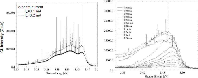
Shown in Fig. 2 (left) are spectra of sample V54, collected with e-beam currents of Ie =100 μA and Ie =200 μA. Optical modes appear within the spectral range of 3.2 to 3.48 eV. Additional scans proved that there is no increment of intensity in any other range. Optical modes of relatively high intensity accumulate between 3.33 and 3.45 eV. The visibility V (V=Imax /Imin , where Imax and Imin are maximum and minimum intensities) is bigger for Ie =100 μA excitation current than for Ie =200 μA. Furthermore, two broad spontaneous emission peaks occur at about 3.395 and 3.45 eV. The apparent optical modes in the emission spectra of sample V60 (MH active region) (Fig. 3, right) differ from the ones of sample V54. Applying current densities of 16 A/cm2 (Ie =80 μA) and above optical modes can be observed. The higher the excitation current densities are, the higher the number of modes and the broader and more intense the spontaneous emission envelope becomes. Increasing the current density from 2 to 16 A/cm2 results in a 4 meV redshift of the emission envelope maximum. The redshift between 16 and 41 A/cm2 (Ie =80 μA and Ie =200 μA) is 14.7 meV.

Figure 2: Emission spectra of sample V54 (GaN: Si active region) (left) and the emission spectra of sample V60 (GaN/Al0.08Ga0.92N active region) (right).
Above an excitation current density of 41 A/cm2 the spontaneous emission intensity increases in the lower energy tail, but it breaks down in the range near 3.45 eV, where optical modes become more intensive, which increases their visibility.
We suggest that the observed modes result from multiple reflections of amplified spontaneous emission (ASE) between the ends of the Fabry-Perot cavity formed by the DBRs. This effect has been previously discussed [Reference Nathan10] in the case of GaAs lasers, and has also been reported in the context of meandering off-axis rays in VCSELs [Reference Bogdankevich11], which by ASE in transverse direction cause an increase of the laser threshold value.
The energy transfer from the emission envelope into a number of optical modes is evidenced by increased mode visibility and diminished envelope intensity around 3.4 eV (Fig. 2, right). Binet et al. [Reference Binet and Briot12] ascribed the appearance of multiple modes in emission spectra, obtained by optical pumping of GaN/InGaN heterostructures to stimulated emission in the etched lateral Fabry-Perot cavity. Assuming maximum quantum efficiency of the radiative transition the maximum energy efficiency of an EBP semiconductor laser is 33%. Only a third of the implanted average energy 〈E〉 = 3 Eg can be transformed into photons by radiative recombination [Reference Bogdankevich11].
We attribute the redshift of the spontaneous emission background maximum of sample V60 to bandgap renormalization. The bandgap shrinkage results from manybody interaction, when the density of the electron-hole plasma (EHP) increases [Reference Bogdankevich11,Reference Nasibov and Shemchuk13,Reference Singh14]. At high nonequilibrium carrier densities, the free carriers begin to screen the deformation potential of the electron-phonon interaction [Reference Bogdankevich11]. Consequently, the thermalisation time τ is increased, i.e. the transfer of energy to the lattice is reduced. Therefore, the temperature of the EHP rises relatively to the lattice temperature (The distribution of the kinetic energy of hot carriers by Coulomb interaction determines the effective temperature). The heating of the quasiequilibrium EHP is a limiting factor for the efficiency of radiative recombination. If the lifetime τ becomes of the order of the spontaneous lifetime τ sp , i.e. the lifetime of the EHP, the threshold power for lasing is increased and population inversion can be prevented.
The excited region of the sample also experiences a quasiadiabatic heating [Reference Nasibov and Shemchuk13,Reference Schiller, Heisig and Panzer15], if the excitation time is smaller than the time the temperature distribution needs to expand over the e-beam cross-section. This condition is fulfilled in our case, so a relative, local temperature rise of several hundred Kelvins also contributes to the bangap shrinkage. In our case it is not evidenced which effect has more influence on the emission redshift nor whether the contributions are of the same order.
The reduced visibility V=Imax /Imin with higher excitation current densities (Fig. 2, right) can be attributed to an effect which strongly influences the propagation of the electromagnetic field within the cavity: the distribution of the nonequilibrium carrier density in the active region, generated by EBP, is inhomogeneous. This implicates a strong inhomogeneity in the gain distribution along the cavity axis. The gain in longitudinally pumped vertical cavities depends on the effective penetration depth [Reference Schiller, Heisig and Panzer15] as shown in equation 1

where Ua is the acceleration voltage. Consequently, the inhomogeneous carrier distribution influences the emission efficiency and the laser threshold as follows [Reference Bogdankevich11]: the carrier density in the most excited, active region is considarably higher than in the passive part. A carrier-density induced bandgap shrinkage occurs in the highly excited region and shifts the gain profile towards longer wavelenghts. This reduces the resonant absorption in the passive part, so that the active transition is out of resonance with the reverse transition. If the pumping becomes larger, the density of free carriers in the weakly excited part increases because of the reabsorption of radiation. This leads to an equalisation of the gain profile along the cavity axis and enhances the losses for the propagating field, unless the optical field is below the saturation value (in that case the passive region becomes transparent).
In contrast to sample V54 with GaN bulk active region, the use of MH structures (V60) minimizes this effect, because the bandgap of the passive region is slightly larger than in the active region. Therefore, the use of quantum wells or quantum dots as active part of the cavity is to be preferred for prevention of gain deterioration.
The deterioration of gain in EBP semiconductor lasers is also attributed to ASE propagating in the transverse direction [Reference Khurgin and Davids16]. The transverse single-pass gain is several times larger than the longitudinal single-pass gain. With increasing diameter of the excited region the threshold value for lasing in longituginal direction increases, because the ASE along the transverse direction of the cavity depletes the longitudinal gain.
These three-dimensional spatial and spectral gain inhomogeneities [Reference Khurgin and Davids16] may also have caused the relative minimum in the spontaneous emission spectrum of sample V54 (Fig. 2, left), located at about 3.43 eV. We assume that the peaks at 3.395 and 3.45 eV indicate recombination of an EHP and phonon-assisted exciton decay at higher photon energy. This has also been observed for optically pumped GaN epilayers [Reference Holst and Hoffmann17], where a further contribution of band-to-band transitions to the high energy emission peak is assigned.
The results of the reflection measurements of V51 and V52 are shown in Fig. 3 (left). The spectrum of V51 reveals a maximum reflectivity of 43% at 364 nm. Sample V52 shows a maximum reflectivity of 43% at 387 nm. The peak located at 364 nm reveals a reflectivity of 34%. Transfer-matrix simulations were done with dispersion data from reflection and transmission measurement on single GaN and AlGaN layers. The obtained values for the reflection maxima are 56% at 380 nm (V52) and 48% at 365 nm (V51). The experimental values are 23% and 10% smaller than the simulated values, respectively. We ascribe this to the dispersion data, where losses, probably due to the buffer layer, could not be specified.

Figure 3: Reflectivity vs wavelength of the single DBR stacks V51 and V52 with simulations (left) and reflectivity of upper and lower DBR of sample V60 (right).
Preliminary X-ray diffraction (XRD) ω/ 2Θ -scans hint at a higher than expected AlN content of the quarter wave layers.
Taking into account the lower experimental values of reflectivity, we can estimate the reflectivity of the lower and the upper DBR stacks of V54 and V60. Therefore we simulated the spectra for the bottom and top stack of V60 (Fig. 3, right) with and without the Al cap layer. A maximum reflectivity of 67% results from a single 15.5 period DBR stack. Adding the Al cap layer, the reflectivity of the overall reflector amounts to 90%. In addition, the Al cap layer reduces electron backscattering and prevents supercharging. If we reduce the values for reflectivity by a factor of 0.75, considering the discrepancy between sample and simulation (V51, V52), we obtain 68% for the upper reflector and 50% for the lower reflector.
Apart from the increase in reflectvity of the upper reflector, induced by the Al cap layer, the peaks also broaden. Broadening enables the propagation of mutiple modes, which is observed in our spectra.
As the threshold condition gives the cavity gain necessary to overcome the cavity loss

for any photon energy [Reference Singh14], one obtains a threshold gain gth of about 2250 cm−1 for V54 and 4240 cm−1 for V60, inserting reflectivity coefficients rb = 0.7 and rt = 0.82, cavity length L = 1.2 μm, a confinement factor Γ = 1 (Γ = 0.53) in the case of V54 (V60) and neglecting any internal losses αloss ( free carrier absorption, absorption by the DBRs etc.). AES and SEM measurements show that the accelerated electrons induce a reaction on the surface of the Al cap layer with carbon compounds, which reside in the vacuum chamber at a pressure of ∼2×10⁻⁵ mbar. Electrons with low kinetic energy induce a polymerisation of carbon compounds [Reference Schiller, Heisig and Panzer15] as can be seen in the outer range of the e-beam cross-section. At the center of the e-beam cross-section, the molecular chains fractionize and suppress polymerisation. This is confirmed by profilometry and AES measurements. The Al cap layer did not alter, so we can exclude a decrease of reflectivity of the upper reflector.
Conclusions
Electron beam pumped vertical cavities with active regions made of a GaN epilayer and a MH structure have shown multimode emission. The optical modes indicate multiple reflections of ASE within the cavity, which is confined by 15.5 period GaN/ Al0.25 Ga0.75 N DBRs with reflectivities of about 70% and 50%, respectively. The use of a multiquantumwell (MQW) or quantum dot active region supposedly prevents gain deterioration, which limits the emission efficiency, and therefore reduces the threshold for lasing.
We conclude that fabrication of DBRs based on the AlGaN/AlN-system is a promising way to realize highly reflective mirrors with low absorption in the near UV spectral range.